TrappeD: DRAM Trojan Designs for Information Leakage and Fault Injection Attacks
Abstract
In this paper, we investigate the advanced circuit features such as wordline- (WL) underdrive (prevents retention failure) and overdrive (assists write) employed in the peripherals of Dynamic RAM (DRAM) memories from a security perspective. In an ideal environment, these features ensure fast and reliable read and write operations. However, an adversary can re-purpose them by inserting Trojans to deliver malicious payloads such as, fault injections, Denial-of-Service (DoS), and information leakage attacks when activated by the adversary. Simulation results indicate that wordline voltage can be increased to cause retention failure and thereby launch a DoS attack in DRAM memory. Furthermore, two wordlines or bitlines can be shorted to leak information or inject faults by exploiting the DRAM’s refresh operation. We demonstrate an information leakage system exploit by implementing TrappeD on RocketChip SoC.
Index Terms:
DRAM, Hardware Trojan, RISCV, RocketChip, Information Leakage, Fault InjectionI Introduction
Integrated Circuit (IC) fabrication has become increasingly vulnerable to malicious modifications in the form of Hardware Trojans [1] due to the outsourcing of semiconductor design and fabrication to third party fabrication houses. Ideally, these modifications need to be detected during pre-Silicon verification and post-Silicon testing. But, it is possible to design these Trojans to remain dormant during the test phase and only activate under rare conditions. Once activated, the Trojans perform undesirable operations such as write/retention failures or even leak sensitive data. This threat is of special concern to government agencies, military [2], technology developers, finance, and energy sectors. Recent news regarding the tampering of server motherboards by Chinese manufacturers that affected top US companies like Amazon, Apple etc. [3] provides as a strong motivation to investigate the possibility of hidden components in each step of the design and manufacturing process.
Memory Trojan can lead to read/write/retention failures and information leakage. In prior works, authors have proposed memory Trojan Trigger circuits and payloads that can evade testing phase and cause different failures. A Trojan for embedded SRAM is proposed in [4]. The authors use unique data patterns written to pre-selected address to trigger their Trojan. Note that these unique patterns are not tested during standard post-manufacturing memory tests and thereby remains undetected. That data pattern feeds the input of the Trojan payload transistors which short the data node of a victim SRAM cell to ground and corrupts the data. The feasibility of this Trojan [4] is limited since the payloads require tapping the bitcells which might not be possible since they are very compact. [5] introduces an NVM-based Trojan trigger that leverages the non-volatility of Resistive RAM (RRAM). It possesses unique characteristics e.g., non-volatility and gradual drift in resistance with pulsing voltage. The triggers presented exploits RRAM’s gradual resistance drift under pulsing current and its non-volatility to ensure that the hammering need not be consecutive. This allows the trigger to evade system-level detection techniques.
Designing a small, controllable and undetectable Trojan is the key element to deploy an efficient one. In [6], a capacitor-based analog Trojan trigger, A2, is presented which is controllable, stealthy and small. In [7], another capacitor-based Trojan trigger is proposed which gets activated if a pre-selected address is written with specific data patterns for a specific number of times. The proposed trigger circuit is shown in Fig. 1. The circuit has two inputs, (the address enable signal of a pre-selected address) and (a logic circuit generates based on the data pattern). The work also presents payloads of the Trojan such as fault injection, Denial of Service (DoS) and information leakage attacks on emerging Non-Volatile Memories (NVMs). The advantage of such trigger lies in the fact that it can be hidden in the filler areas of the non-memory logic (e.g., address pre-decoding and pipelining units, also called midlogic) [8]. However, the payload of this Trojan also requires tapping the bitcell.
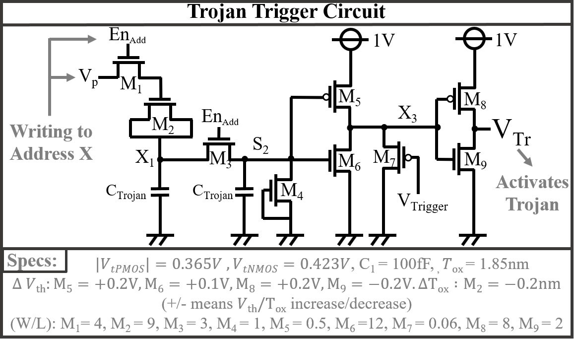
Proposed Attack Model: In this work, we assume an untrusted manufacturing house located outside the US that can alter the chip GDS-II file to introduce the malicious Trojan trigger and payload. This assumption is widely accepted in the hardware security community because of large filler areas present in the chip and the adversary’s access to the raw design. We propose the use of a capacitor-based hardware Trojan trigger [7] and novel payload circuits and perform detailed analysis to guarantee that the Trojan is, (i) triggered even under worst-case process and temperature conditions with correct inputs; (ii) able to bypass conventional post-manufacturing test. The Trojan is activated if a particular pre-selected address of L1 Cache is accessed for 1800 times. Note that the proposed Trojan trigger directly taps the wordline of the pre-selected address to leverage the existing decoder design framework and hence, does not incur any overhead for address decoding.
In summary, the following contributions are made in this paper.
-
(a)
Investigate DRAM peripherals and their security implications;
-
(b)
Propose a novel Trojans in DRAM that can leak the data by exploiting the column multiplexing and self-refresh properties;
-
(c)
Propose Trojans in DRAM that can tamper with refresh mechanism for polarity dependent fault injection;
-
(d)
Demonstrate TrappeD exploits in action using an open-source RocketChip SoC system.
The paper is organized as follows: Section II reviews the basics of DRAM design and operation; Section III describes the proposed trojan trigger design and analysis; Section IV describes the DRAM vulnerabilities and the attack details; Section V describes the system implementation to validate the proposed Trojan attacks; Section VI presents discussions on the practicality, assumptions, and countermeasures to TrappeD; and finally Section VII draws the conclusion.
II Background
II-A Basics of DRAM
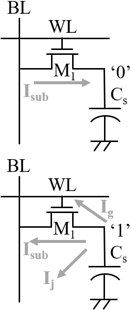
Fig. 2(a) shows a basic one-transistor, one-capacitor (1T1C) DRAM cell. The data is stored as charge in the capacitor . The charge corresponding to (0V) is considered as data ‘1’ (‘0’). The capacitor gradually leaks or charges up over time and thereby, it requires to be read and written-back (i.e., refresh).
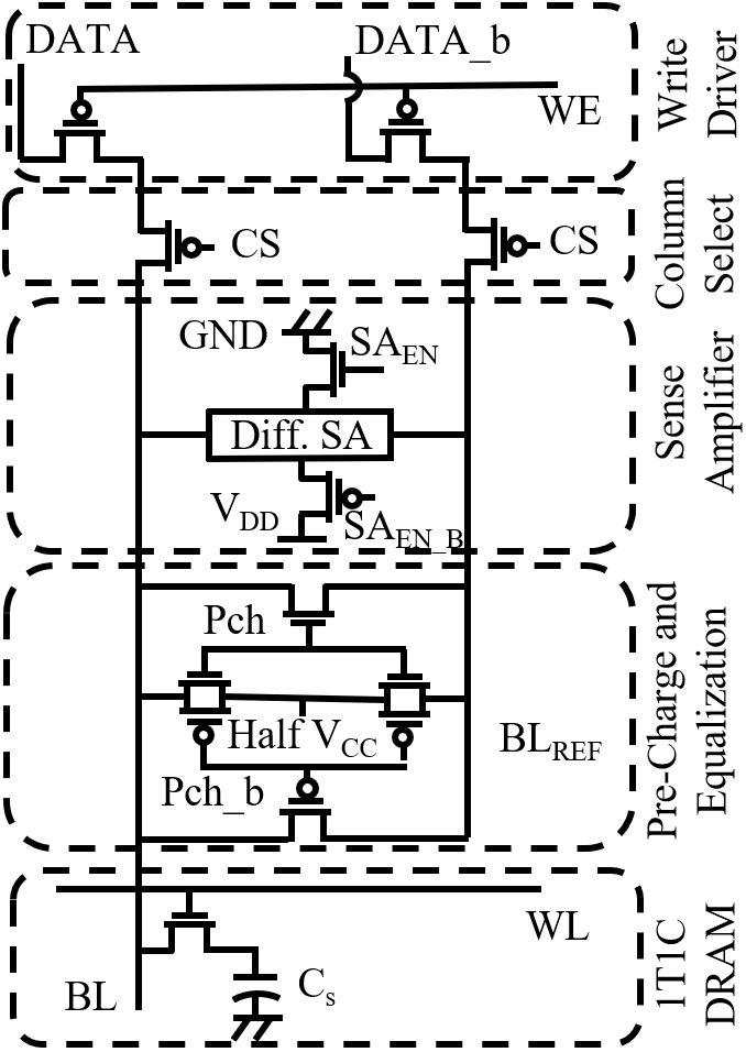
Architecture: Fig. 2(b) shows the column structure of an open bitline architecture [9]. It includes DRAM bitcell, , reference bitline (), sense amp, precharge circuit, column select, write driver and generator.
The column circuit is implemented with the following features: a) Sense amp is placed on per-local-column basis to enable read/refresh of the selected column during read and refresh half-selected columns during write; b) Sense amp is activated by enabling both the header and footer transistors to prevent static current due to bitline precharge; c) The precharge and equalization circuit (equalizes and voltages) consists of full CMOS pass transistors; and d) is boosted (to 1.6V in this paper) to write a full ‘1’ through the NMOS access transistor and under-driven (to -0.2V in this paper) to reduce sub-threshold leakage during retention. Positive and negative charge pumps are used for overdrive and underdrive respectively; and e) Column selection uses PMOS switch.
DRAM operation: The DRAM operation can be classified into the following categories [10]:
Write: During write, the access transistor (Fig. 2(a)) is turned ON by asserting the . The is driven to (0V) for writing data 1 (0). The storage capacitor charges up (discharges) to (0V) based on voltage. Writing data ‘0’ is accomplished by first writing a good ‘1’ on the while the stays close to (threshold voltage of PMOS transistor) and then firing the sense amp. Once the sense amp is ON, it pulls the all the way to 0V and a good ‘0’ is written to the bitcell.
Read: This begins with pre-charging the and to and then the is turned ON. The charge stored in charges (discharges) the if the stored data is ‘1’ (‘0’). Therefore, also develops a differential and loses its stored value (destructive read). The resulting voltage differential in the is converted to a digital value by the sense amp that compares the to the reference voltage .
Write-back: Following the differential development, the sense amp is enabled. The resolves to (0V) and resolves to 0V () if the read value is ‘1’ (‘0’). The bitcell is restored to original value since the is still ON after resolves to the read value.
Stand-by (Retention): A data ‘1’ would lose its value once the charge reduces below . Note that this very optimistic assumption. In reality, the sense amp requires 70mV of Sense Margin (SM) which puts maximum leakage of data ‘1’ to 0.640V. Three major sources of leakage are sub-threshold (), junction (), and gate leakage () through the access transistor (Fig. 2(a)). Data ‘0’ can lose its value if it charges above 0.360V (to guarantee 70mV of SM). The only source of leakage for data ‘0’ is . In our model, the charge stored in only rises up to 30mV after which the rate of charging due to equals the rate of capacitor discharge. Therefore, data ‘0’ does not suffer from retention issues.
III Trojan Trigger Design
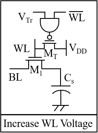
Design [7]: The trigger circuit (Fig. 1) [7] is designed to be activated if a particular memory address (chosen during design phase, let’s call it ) is accessed for at least times. The trigger has two inputs namely, and . (= 1V in this work) is the wordline enable signal of and is a constant voltage source of 1V. For a more complex Trojan with a superior stealthiness, can be programmable (refer to Section IV-B for details).

Whenever is accessed, is asserted and MOSFETs and are activated. has a thinner gate oxide compared to other MOSFETs and its source and drain are shorted. Therefore, works as a capacitor and charges from the source through Fowler Nordheim (FN) tunneling [11] if is asserted. is an OFF transistor which offsets gate leakage of and prevents unwanted charging-up of node . keeps node as low as possible until node charges up sufficiently. The node , that is charged up during the hammering process, is used as the SET input of a SR latch. The output of the SR latch () transitions from when charges up to 0.5V. The signal is then used to activate the Trojan.
The charge at node leaks away (due to capacitance leakage of ), once the hammering is discontinued. However, will still be asserted due to the SR latch. In order to deactivate the Trojan, needs to be asserted. can be generated by accessing a different address (let’s say ) for at least times and using a circuit similar to the trigger one. Note that a smaller (1fF) can be used in the RESET circuit to minimize the area overhead which leads to 92. However, the AND’ed output of and can also serve as which further reduces the area overhead.
Simulation results: Node charges up to 125mV (steady state) from all the leakage considering = 1V (worst-case charging due to leakage). This value is not enough to trigger the circuit. For the rest of the simulation, we have considered that is a pulse source with ON/OFF time of 10ns/1ns. We consider the circuit to be triggered when reaches up to 0.5V. We started our analysis with = 20fF.
Fig. 4(a) shows the design space exploration of trigger circuit considering two variables, the (W/L) ratios of MOSFETs and . For a lower (W/L) ratio for both the MOSFETs, increases. We have chosen (W/L) of and as 4 and 2 respectively for a sufficiently higher .
Next, we considered that the adversary accesses the preselected address for = 10 and then stays idle for = 1/3/…/21/23 and repeats this cycle. We found that the does not significantly leak in the OFF cycle and the circuit can still be triggered with a higher (Fig. 4(b)). We observe that the circuit will trigger even with a low of 30. This means that it becomes harder to prevent Trojan activation using system level techniques such as limiting repeated access to one address.
Note that the attack gets auto reset without the SR latch since the node discharges (due to charge leak of ) and eventually node goes down once the adversary stops the hammering after the trigger activates. Results indicate that the attack (charge at node ) lasts for 163.73s if is accessed for 18s. However, by adding the SR latch, the attack can last indefinitely until access is discontinued and is asserted.
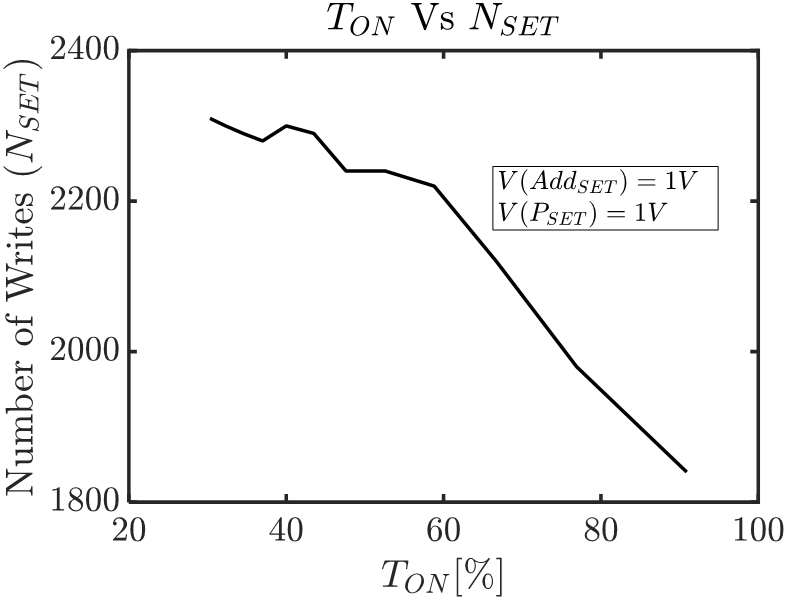
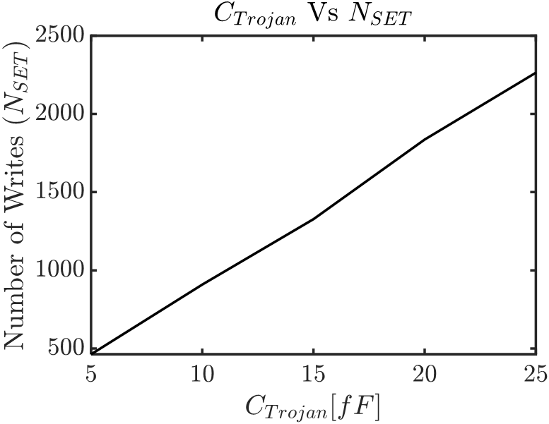
A small will require a low to get the trigger activated. For example, the required number of access, = 464 for = 5fF (Fig. 4(c)). This is still significantly high enough to evade the test phase. The value of is chosen as 20fF since it offers a high (= 1837) under nominal conditions, successfully triggers under all process corners and temperatures (-10°C to 90°C) and minimum in the worst-case (= 68) is still high to evade testing phase.
Table I summarizes the key performance metrics of the trigger. The absolute area and static power of proposed trigger are 42.95m2 and 0.589W, respectively which are 5.3410-5% and 6.2410-5% of a typical memory chip area and static power [12], respectively. Therefore, the overhead due to the trigger is negligible to be detected via optical inspection or side channel analysis.
| Parameter | Trojan Trigger |
|---|---|
| Dynamic Power (W) | 3.781 |
| Static Power (W) | 0.589 |
| Energy/hammer (nJ) | 2.059 |
| Area (m2) | 42.97 |
| Target | 1837 |
| Worst-Case | 1502 |
IV DRAM Vulnerabilities and Trojans
In this section, We present methods to exploit the vulnerabilities of the DRAM assist techniques and refresh mechanisms.


IV-A DRAM assist and vulnerabilities
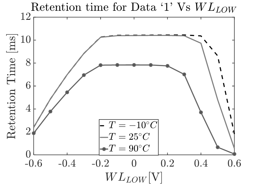
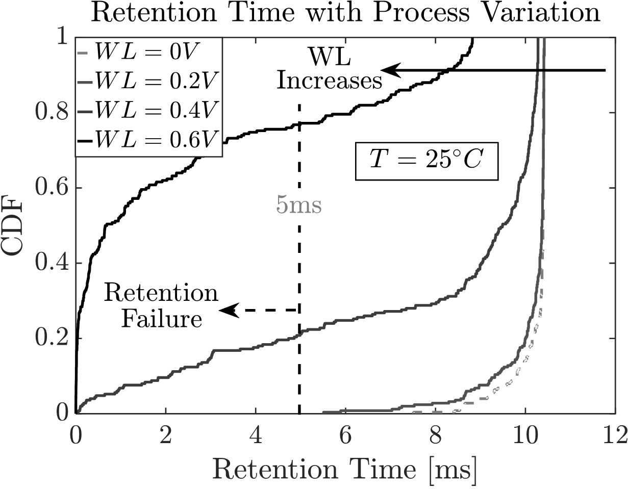
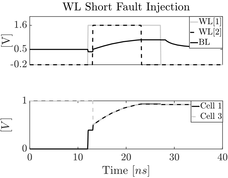
Wordline Underdrive and DoS: Fig. 5(a) shows that the retention time of data ‘1’ changes as the voltage during retention is swept. The worst case retention occurs at higher temperature. We consider retention failure if the capacitor discharges below . Note that retention time decreases below -0.2V (due to Gate Induced Drain Leakage (GIDL)) and above 0.3V (due to subthreshold leakage) for each of the operating temperatures. The adversary cannot lower the voltage below -0.2V since this is the lowest voltage available in the chip. However, adversary can increase the voltage during retention. The can be connected to through the transistor (Fig. 6(a)). The gate of is controlled by the AND’ed signal of (from Fig. 1) and (Fig. 6(a)). is used in order to ensure that the underdrive only occurs during retention.
We have performed 1000 point Monte-Carlo simulation with the same setup as SRAM to investigate the impact of increased voltage during retention. We consider retention time below 5ms as failure. From Fig. 5(b), we note that if the adversary increases voltage to 0.3V and 0.4V respectively from -0.2V during retention, the corresponding retention failure is 4.8% and 43.6% respectively, causing polarity fault injection attack.
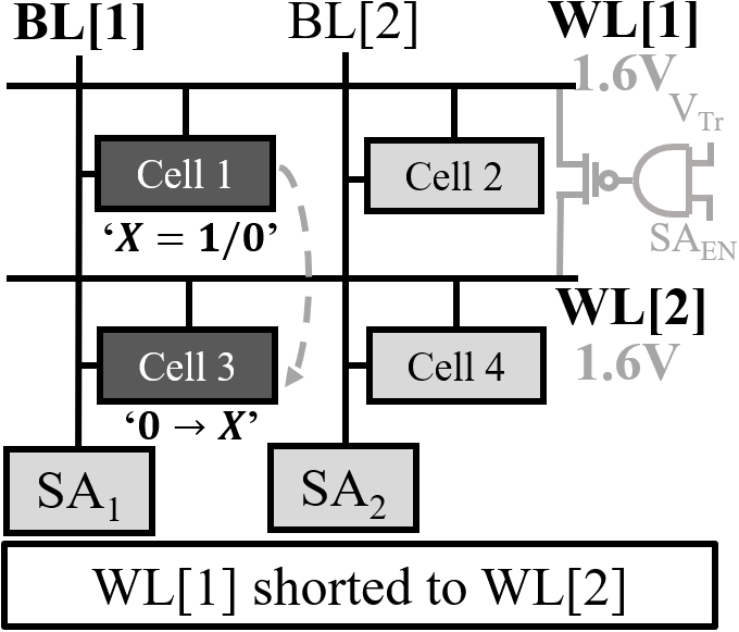
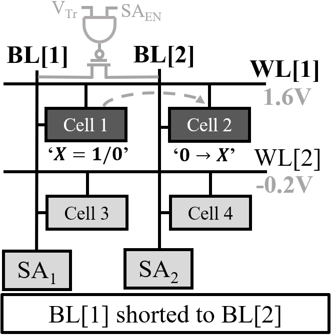
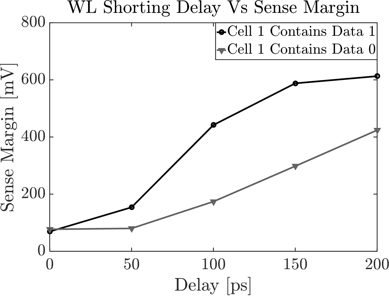
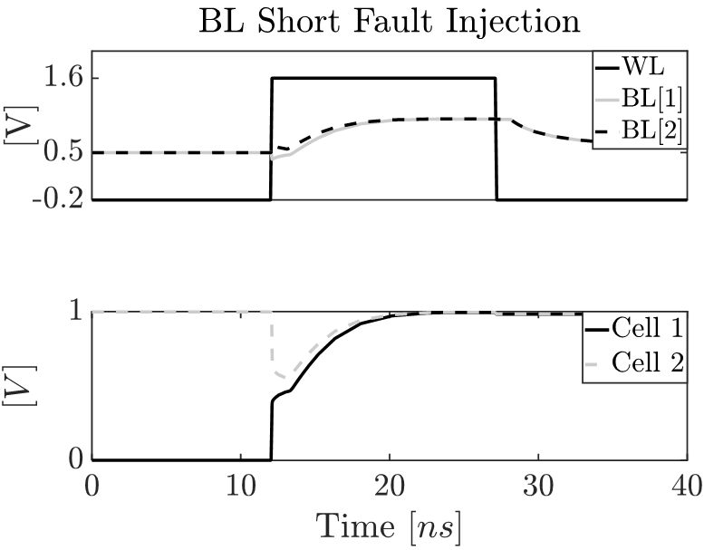
Information Leakage - Shorting and Refresh: Fig. 3(a) shows the method to short and . It is assumed that victim and adversary have control over Cell 1 and Cell 3, respectively. The shorting transistor is controlled by the AND’ed signal of and . is used to ensure that the are shorted only after the sense amp is fired. This delay gives the sense amp sufficient differential between and and ensures Cell 3 value does not corrupt Cell 1 (during sensing) that is being copied. In the AND Trojan, we get a delay of 40ps which provides a SM of 69mV. For larger SM an inverter chain can be used. Fig. 6(b) shows that SM for both data type increases with delay. Note that driver should be disabled during the shorting period.
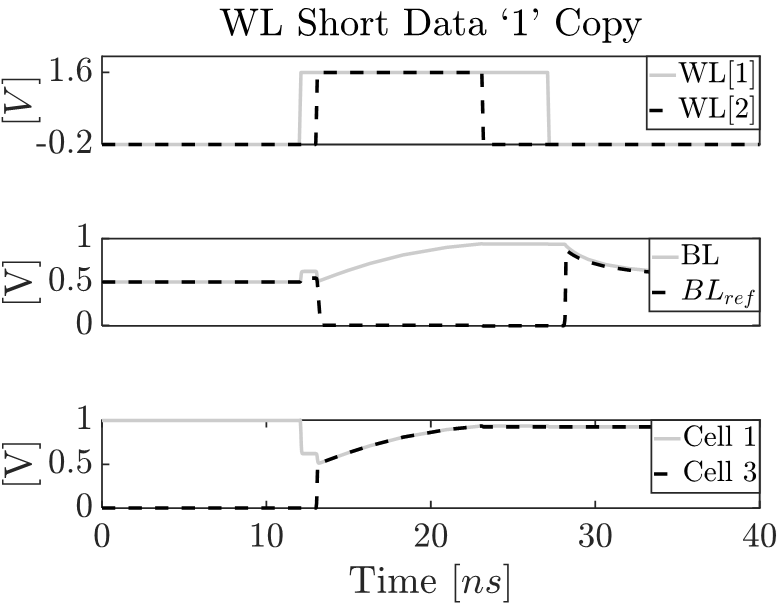
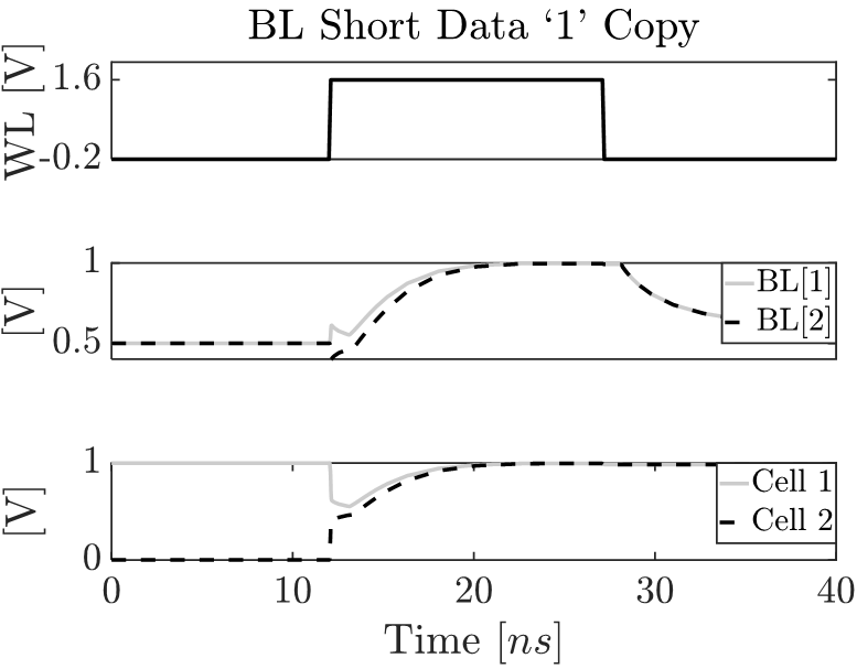
When is asserted to 1.6V during a read operation of Cell 2, is also pulled to 1.6V after the sense amp firing. Since DRAM read operation is destructive and needs a write-back at the end of read operation, will resolve according to the stored value in Cell 1. Therefore, both Cell 1 and Cell 3 will get written to the previously stored value in Cell 1 since their are asserted. This will effectively copy the data to Cell 3.
Fig. 7(a) shows when Cell 3 is initialized to ‘0’ and data in Cell 1 is read as ‘0’. Both Cell 1 (due to write-back) and Cell 3 are written to ‘0’. Similarly, Fig 7(b) shows that data in Cell 1 is read as ‘1’ and both Cell 1 and Cell 3 are written to ‘1’. This data leak also applies when Cell 3 is initialized to ‘1’. If shorting occurs with no delay after the sense amp activation, both Cell 1 and Cell 3 are written to Cell 3 data irrespective of the original Cell 1 data as shown in Fig. 8(a). This can be done to inject a polarity dependent fault to Cell 1. Furthermore, the information leakage attack also works if write operation is performed to Cell 1 since the will be driven to or 0V based on the write data and both and are shorted. One important point to note that all the cells sharing will be corrupted in this process.
Information Leakage - Shorting and Refresh: shorting is carried out in a similar way to shorting (Fig. 3(b)). It is assumed that victim and adversary have control over Cell 1 and Cell 2, respectively. The explanation for shorting holds true for shorting except none of the cells will be corrupted (since all the cells sharing will be refreshed). Fig. 7(c) shows that the data in Cell 1 is read as ‘0’ and both Cell 1 (due to write-back) and Cell 2 (due to shorting) are written to ‘0’. Fig. 7(d) shows the copy of data ‘1’. Similar to shorting, shorting can also be leveraged to inject a polarity dependent fault in Cell 1 as shown in Fig. 8(b). We restrict our discussion on this for the sake of brevity.
IV-B Trojan design space exploration
We choose the capacitor-based trigger proposed in [7] to generate the trigger signal () required to induce the retention failures (Fig. 6(a)) and information leakage (Fig. 3) attacks. This is because the design allows easy change of trigger parameters to vary the number of address accesses (denoted by ) required to assert . We modify the design parameters shown in Fig. 1 to allow the trigger design to stay undetected at all fast and slow corner cases and work under multiple temperatures (-10C,25C, and 90C). The modified design is shown in Fig. 1. Additionally, we include an SR latch to capture the trigger output.Note that the attack gets auto reset without the SR latch since the node discharges (due to charge leak of ) and eventually node discharges once the adversary stops the hammering after the trigger activates. Results indicate that the attack (charge at node ) lasts for 163.73s if is written for 18s with = 1V, = 1V. However, by adding the SR latch, the attack can last indefinitely until access is discontinued and is asserted.
V System Exploits using TrappeD
V-A Overview of systems architecture
For the purposes of demonstration, we show a simple information leakage attack using TrappeD. We use a RISC-V based RocketChip [13] SoC template for implementing the TrappeD system. Our RocketChip SoC is configured with an in-order Rocket Core, a fast L1 data cache, and connects to an external DRAM on the AXI port (mapped to 0x80000000), which serves as the main memory for the system.
V-B TrappeD trojan deployment
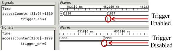
We modified the RocketChip code to inject the Trapped trigger and payload. The trigger logic is introduced in the D-cache and the payload logic in the DRAM. For modelling the effects of trigger, we instantiate a 32-bit register (AccessCounter) that is initialized to ‘0’. Accesses to the trigger address (= 0x80022328) increments the register value by ‘1’. We introduce logic to detect if these increments have reached our threshold of 1837, to active the trigger signal (trigger_en). The trigger signal is sent to the payload logic. Once triggered, the signal stays asserted to facilitate the attack till the adversary accesses the trigger address an additional 163 times. The waveform generated from the RocketChip hardware emulation depicting trigger_en enabled and disabled is shown in Fig. 9. The payload activates when trigger_en is high. To model the effects of the payload, we select two addresses: (i) an adversary controlled address, adversary (= 0x800222E8), and (ii) a victim address, victim (= 0x800222A8). The payload logic shorts the two addresses, effectively copying the data from victim to adversary, facilitating an information leakage attack.
V-C Attack demonstration
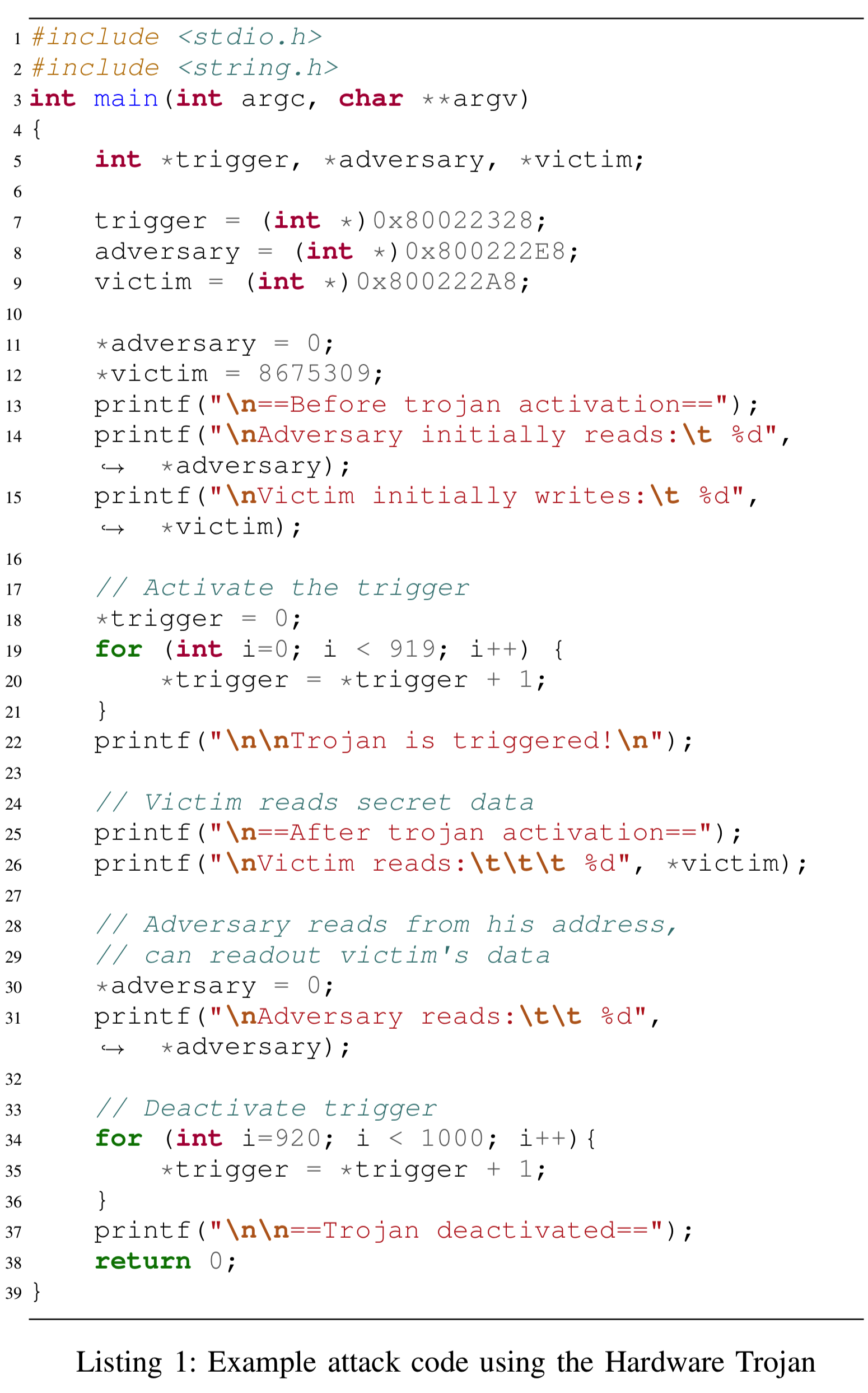
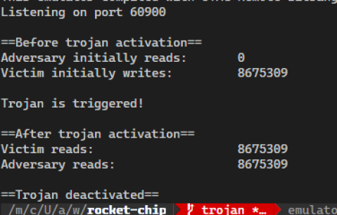
We demonstrate the attack with the help of a simple C program as shown in Listing 1. The code is compiled with the riscv-gcc compiler to generate a RISC-V ELF binary that can be run on the cycle-accurate emulator for the RocketChip system. For simplicity, we have assumed that the adversary and victim addresses are part of the same process, and the adversary can access adversary, but not victim. We also assume that the adversary has control over the number of times the trigger address can be accessed. The program initializes contents of adversary to ‘0’ and victim to the confidential information ‘8575309’. The program loops over and accesses trigger 1837 times, which is greater than the minimum accesses required by the Trojan trigger as set by , thus activating the trigger_en signal. The payload causes an information leakage by copying the confidential contents of victim to adversary. The adversary can now read out from adversary address and thus reveal the confidential information ‘8675309’, as shown in Fig. 10.
VI Discussion
VI-A Fault injection and DoS Attack
If read/write/retention failure occurs for one polarity (either for data ‘0’ or ‘1’), it is considered as fault injection. Such attack can leak system assets [14] such as, keys. One example is setting plaintext to all 0 or 1 by injecting faults during crypto operation which makes the ciphertext (that is sent out) same as keys, and can be recovered by the adversary. However, if failure occurs for both polarities, it is considered as DoS attack.
VI-B Bypassing error detection
In state-of-the-art memory, techniques like Cyclic Redundancy Check (CRC) or Error Correcting Code (ECC) [15] is implemented. The ECC and/or CRC word is computed for the raw data and written along with data during write operation. During read operation, CRC/ECC is again calculated based-on the read data and matched with the stored CRC/ECC. If read or even write operation incurs an error, CRCs/ECCs will not match and the data can be discarded. Furthermore, ECC can correct 1/2 bits of error (based on the implementation). Therefore, fault injection will fail and adversary can only launch DoS attack. However, if the CRC or ECC bits are also tampered to match the data with injected fault, the manipulated data will be considered as valid data.
VI-C Possible defenses
i) Dummy Bits: Each row of the memory can be designed with few dummy bits. During run-time, each row can be written with known dummy bits and read to validate. During Trojan induced fault/DoS, the dummy bits will fail which can be detected as an attack. However, information leakage cannot be detected. Note that this will incur slight area and power overhead.
ii) Trusted ECC: The current implementation of ECC adds a few global columns in the memory. For example, if the data width is 64 bit and ECC needs 5 bits, a total of 69 global columns are implemented in the memory array. This is a vulnerability since the ECC bits can also be tampered. We propose to separate the ECC bits from the data bits and store them in a trusted memory known to be Trojan free through rigorous validation (possible due to small size). This way the fault injection, DoS and information leakage attacks can be detected since ECC bits can be checked to detect the tampering at run-time (once Trojan is activated).
VII Conclusions
In this paper, we investigated the advanced circuit features employed in the peripherals of nanometer memories e.g., WLUD and wordline overdrive for DRAM from a security perspective. We show that an adversary can manipulate these features to launch fault injection attacks and DoS. The adversary can also leverage wordline shorting and bitline shorting in order to leak sensitive information. We also demonstrated the feasibility of launching system exploits leveraging TrappeD on RocketChip SoC platform.
Acknowledgements: This work is supported by SRC (2847.001), NSF (CNS- 1814710, CNS- 1722557, CCF-1718474, DGE-1723687 and DGE-1821766) and DARPA Young Faculty Award (D15AP00089).
References
- [1] S. Bhunia and M. Tehranipoor, The Hardware Trojan War: Attacks, Myths, and Defenses. 01 2018.
- [2] “Trusted Integrated Circuits (TRUST). [Online]. Available: https://www.darpa.mil/program/trusted-integrated-circuits. Accessed: Oct 28, 2018,” 2018.
- [3] “The Big Hack: How China Used a Tiny Chip to Infiltrate U.S. Companies. [Online]. Available: https://bloom.bg/2owldii. Accessed: Oct 28, 2018,” 2018.
- [4] T. Hoque, X. Wang, A. Basak, R. Karam, and S. Bhunia, “Hardware Trojan Attacks in Embedded Memory,” in 2018 IEEE 36th VLSI Test Symposium (VTS), pp. 1–6, April 2018.
- [5] K. Nagarajan, M. Khan, and S. Ghosh, “ENTT: A Family of Emerging NVM-based Trojan Triggers,” Proceedings of the 2019 IEEE International Symposium on Hardware Oriented Security and Trust, HOST 2019, (United States), pp. 51–60, Institute of Electrical and Electronics Engineers Inc., 5 2019.
- [6] K. Yang, M. Hicks, Q. Dong, T. Austin, and D. Sylvester, “A2: Analog Malicious Hardware,” in 2016 IEEE Symposium on Security and Privacy (SP), pp. 18–37, May 2016.
- [7] M. N. Imtiaz Khan, K. Nagarajan, and S. Ghosh, “Hardware Trojans in Emerging Non-Volatile Memories,” in 2019 Design, Automation Test in Europe Conference Exhibition (DATE), pp. 396–401, March 2019.
- [8] U. Bhattacharya, Y. Wang, F. Hamzaoglu, Y. Ng, L. Wei, Z. Chen, J. Rohlman, I. Young, K. Zhang, “45nm SRAM Technology Development and Technology Lead Vehicle,” in Intel Technology Journal, vol. 12, pp. 111–120, June 2008.
- [9] D. Wang, S. Ng, and B. Jacob, “DRAM Device Organization: Basic Circuits and Architecture,” Memory Systems, pp. 353–376, 2008.
- [10] S. Ghosh, “Modeling of Retention Time for High-speed Embedded Dynamic Random Access Memories,” IEEE Transactions on Circuits and Systems I: Regular Papers, vol. 61, pp. 2596–2604, Sep. 2014.
- [11] N. M. Ravindra and J. Zhao, “Fowler-Nordheim Tunneling in Thin SiO2 Films,” Smart Materials and Structures, vol. 1, pp. 197–201, sep 1992.
- [12] M. Chang, P. Rosenfeld, S. Lu, and B. Jacob, “Technology Comparison for Large Last-level Caches: Low-leakage SRAM, Low Write-energy STT-RAM, and Refresh-optimized eDRAM,” in 2013 IEEE 19th International Symposium on High Performance Computer Architecture (HPCA), pp. 143–154, Feb 2013.
- [13] K. Asanovic, R. Avizienis, J. Bachrach, S. Beamer, D. Biancolin, C. Celio, H. Cook, D. Dabbelt, J. Hauser, A. Izraelevitz, S. Karandikar, B. Keller, D. Kim, J. Koenig, Y. Lee, E. Love, M. Maas, A. Magyar, H. Mao, M. Moreto, A. Ou, D. A. Patterson, B. Richards, C. Schmidt, S. Twigg, H. Vo, and A. Waterman, “The Rocket Chip Generator,” Tech. Rep. UCB/EECS-2016-17, EECS Department, University of California, Berkeley, Apr 2016.
- [14] S. Bhattacharya and D. Mukhopadhyay, “Formal Fault Analysis of Branch Predictors: Attacking Countermeasures of Asymmetric Key Ciphers,” Journal of Cryptographic Engineering, vol. 7, pp. 299–310, Nov 2017.
- [15] G. Asadi and M. B. Tahoori, “Soft Error Mitigation for SRAM-based FPGAs,” in 23rd IEEE VLSI Test Symposium (VTS’05), pp. 207–212, May 2005.