Influence of electron-vibration interactions on electronic current noise
of atomic and molecular junctions
Abstract
We present an ab-initio method to simulate the current noise in the presence of electron-vibration interactions in atomic and molecular junctions at finite temperature. Using a combination of nonequilibrium Keldysh Green’s function techniques and density functional theory, we study the elastic and inelastic contributions to electron current and shot noise within a wide range of transmission values in systems exhibiting multiple electronic levels and vibrational modes. Within our model we find the upper threshold, at which the inelastic noise contribution changes sign, at a total transmission between and for gold contacts. This is higher than predicted by the single-level Holstein model but in agreement with earlier experimental observations. We support our theoretical studies by noise measurements on single-atom gold contacts which confirm previous experiments but make use of a new setup with strongly reduced complexity of electronic circuitry. Furthermore, we identify 1,4-benzenedithiol connected to gold electrodes as a system to observe the lower sign change, which we predict at around . Finally, we discuss the influence of vibrational heating on the current noise.
KEYWORDS: single-atom junction, single-molecule junction, shot noise, electron-vibration interaction, density functional theory, mechanically controlled break junction
I Introduction
Shot noise is a nonequilibrium fluctuation phenomenon, which is caused by the discreteness of charge carriers Blanter and Büttiker (2000); Beenakker and Schönenberger (2003); Cuevas and Scheer (2017). When the size of an electronic system reaches the nanometer scale, it becomes an important tool for exploring correlations in charge transport de Picciotto et al. (1997); Saminadayar et al. (1997); Cron et al. (2001); Zhou et al. (2019) or for detecting temperature differences on the atomic scale Lumbroso et al. (2018). Shot noise reveals additional information on the electronic structure and transport properties, like the number of open transmission eigenchannels and their transmissions, which cannot be obtained by conventional studies of the conductance Reznikov et al. (1995); van den Brom and van Ruitenbeek (1999); Djukic and van Ruitenbeek (2006); Kiguchi et al. (2008); Schneider et al. (2010, 2012); Kumar et al. (2013); Ben-Zvi et al. (2013); Vardimon et al. (2013); Karimi et al. (2016a). Besides shot noise, also low-frequency flicker noise contains valuable information on the type of transport in nanoscale systems, e.g. on ballistic versus diffusive transport or two-level current fluctuations Sánta et al. (2019); Xiang et al. (2015). When the applied voltage vanishes, the Johnson-Nyquist thermal noise dominates, where is the Boltzmann constant, the temperature and the linear conductance. Once the system is biased, it is gradually moved away from equilibrium, and a crossover from thermal to nonequilibrium noise occurs. Assuming phase-coherent elastic charge transport, as described in the framework of Landauer-Büttiker scattering theory, the conductance can be expressed as
| (1) |
and the noise power as Büttiker (1992); Blanter and Büttiker (2000); Cuevas and Scheer (2017)
| (2) |
where is the elementary charge, the quantum of conductance, the applied bias voltage, the transmission probability of the th transmission eigenchannel, the number of allowed transmission eigenchannels, and . In Eq. (1) we use the total transmission
| (3) |
When , the noise power is reduced to its classical shot noise form . Here is the time-averaged current, while
| (4) |
is the Fano factor that describes the dependence of on the individual transmission probabilities .
From Eq. (2) it is clear that for a perfect transmission of all channels ( for ) shot noise is suppressed, because there are no fluctuations in the occupation numbers of left- and right-moving electrons. This picture of elastic transport with non-interacting electrons was confirmed experimentally for nanostructures and mesoscopic conductors in general on many occasions Blanter and Büttiker (2000); Agraït et al. (2003); Cuevas and Scheer (2017); Song and Lee (2017); Evers et al. .
Nontrivial deviations from elastic scattering theory are expected as the bias voltage exceeds the threshold for excitation of vibrational modes. The study of electron-vibration (EV) scattering in nanoscale systems, especially atomic and molecular junctions, has become an important tool to determine the precise contact geometry and to identify the molecule that bridges two metal electrodes. It can be addressed experimentally by point-contact spectroscopy Agraït et al. (2002); Smit et al. (2002); Agraït et al. (2003), inelastic electron tunneling (IET) spectroscopy Kushmerick et al. (2004); Wang et al. (2004); Galperin et al. (2004); Smit et al. (2002); Djukic and van Ruitenbeek (2006); Song et al. (2009); Kim et al. (2011); Karimi et al. (2016b) or Raman spectroscopy Ioffe et al. (2008); Ward et al. (2010); Bi et al. (2018). Point-contact and IET spectroscopy are identical techniques, but the names originate from the different high and low conductance ranges, respectively, in which they are applied.
Theory has made major contributions to the better understanding of the influence of inelastic EV interactions on charge current. Using a Hamiltonian with a single electronic level coupled to two electrodes and a single vibrational mode, which we will refer to in the following as single-level Holstein model (SLHM), observations of point-contact and IET spectroscopy could be understood in a unified framework de la Vega et al. (2006); Paulsson et al. (2005, 2008); Cuevas and Scheer (2017). Thus, a transition from a step up to a step down in the differential conductance has been predicted with increasing transmission as the bias voltage is swept across the vibrational energy from below. For symmetric single-channel junctions and weak EV coupling the sign change in the differential conductance takes place at , with a corresponding decrease for asymmetrically coupled junctions de la Vega et al. (2006); Paulsson et al. (2005, 2008); Cuevas and Scheer (2017). Subsequent theory work was directed towards inclusion of strong EV couplings Schinabeck et al. (2016) and towards material-specific predictions that take multiple electronic levels and vibrations as well as the coupling between them into account Frederiksen et al. (2007); Bürkle et al. (2013). To avoid free parameters, ab-initio electronic structure theory, in particular DFT, has been employed to obtain the electronic Hamiltonian, vibrational modes and corresponding EV couplings Frederiksen et al. (2007); Bürkle et al. (2013). The theoretical predictions of the sign change in inelastic conductance corrections have been confirmed experimentally for different systems Tal et al. (2008); Kim et al. (2011).
Similar to point-contact, IET or Raman spectroscopy of the current, inelastic current noise of atomic-scale junctions provides unique information on the system such as the local phonon population. Therefore the studies of inelastic EV interactions have subsequently been extended to shot noise. Using the SLHM and assuming weak EV coupling, two transitions at different transmissions have been predicted, at which the step in the first derivative of the inelastic noise contribution with respect to voltage changes sign at the vibrational energy Avriller and Levy Yeyati (2009); Schmidt and Komnik (2009); Haupt et al. (2009). In the case of a symmetrically coupled single-channel junction with the resulting step, as the bias crosses the vibrational energy, is positive, when or , and negative in between Avriller and Levy Yeyati (2009). The predictions remain basically unchanged, if a scattering-state formulation is adopted Kim (2014). For a more realistic picture, the scheme of Ref. Haupt et al. (2009) has later been extended to be compatible with the existing ab-initio approaches, applied to point-contact and IET spectra, as described above. Using the lowest-order expansion of the shot noise in the EV coupling, it takes multiple electronic levels, vibrational modes and all relevant EV couplings into account Haupt et al. (2010). This formulation was utilized in Ref. Avriller and Frederiksen (2012) to study both the elastic and inelastic shot noise in gold (Au) and platinum (Pt) metallic atomic contacts within a parameter-free DFT simulation. Inelastic processes strongly alter the high-voltage behavior Novotný et al. (2011); Novotný and Belzig (2015).
While shot noise in atomic contacts and molecular junctions has already been measured in the elastic low-bias regime van den Brom and van Ruitenbeek (1999); Smit et al. (2002); Djukic and van Ruitenbeek (2006); Kiguchi et al. (2008); Vardimon et al. (2013); Karimi et al. (2016a), the inelastic effects on electronic shot noise due to EV couplings have been analyzed only recently Tsutsui et al. (2010); Kumar et al. (2012); Chen et al. (2014); Xiang et al. (2015); Chen and Natelson (2016); Tewari and van Ruitenbeek (2018); Tewari et al. (2019). Tsutsui et al. Tsutsui et al. (2010) investigated the fluctuations of charge current flowing through a single molecule at K. They report an increased noise signal at voltages that are characteristic for the molecular vibrational modes and find a similar peak structure in both shot noise and IET spectra. Tewari et al. Tewari et al. (2019) recently demonstrated for deuterium molecules that the inelastic noise contributions due to vibrational excitations interacting with two-level fluctuators can be used to detect inelastic processes more precisely than with IET spectra. In the experimental work by Kumar et al. Kumar et al. (2012) the shot noise of Au atomic contacts was measured at liquid helium temperatures. It was discovered that the inelastic noise correction is positive for zero-bias conductance close to , but negative below Kumar et al. (2012). The transition of the inelastic noise corrections from positive to negative at , as predicted by the SLHM, has not been confirmed experimentally yet.
Interestingly, pioneering first-principles calculations of shot noise characteristics in Ref. Avriller and Frederiksen (2012) could not identify the sign change in the correction to the inelastic shot noise, reported in Ref. Kumar et al. (2012). The studied junction structures showed generally transmissions , i.e. above the theoretically expected inelastic sign crossover threshold Kumar et al. (2012) but below the experimentally reported value of Kumar et al. (2012). Based on their calculations, the authors speculated that the crossover might occur at a value even lower than Avriller and Frederiksen (2012).
Hence, there remain several open points. They regard the confirmation of the sign changes at and in ab-initio models as well as the experimental verification of the lower threshold at . On a more quantitative level it is also of relevance to explain the discrepancy between the theoretical sign threshold of and the measured one at Kumar et al. (2012).
In this work we address the aforementioned challenges by investigating inelastic effects in the shot noise of atomic contacts and molecular junctions theoretically and experimentally. Within our newly developed ab-initio approach we detect the noise-sign crossover threshold at a total transmission between and for Au atomic contacts. By numerically studying 1,4-benzenedithiol (BDT) connected to gold electrodes, we predict the crossover of the inelastic noise correction in the low conductance range to occur around . We propose the Au-BDT-Au single-molecule junctions as a system with a widely tunable conductance in order to observe also this low-transmission sign crossover. Finally, we analyze the influence of vibrational heating on the current-noise properties in Au and Au-BDT-Au junctions theoretically, showing a transition from a linear to a quadratic dependence with increasing voltage, depending on the assumed strength of the coupling of the junctions’ vibrational modes to an external reservoir. Our theoretical predictions for Au metallic contacts are supplemented by new experimental data, confirming earlier measurements by Kumar et al. Kumar et al. (2012).
This paper is organized as follows. In Sec. II we will introduce the theoretical and experimental methods that we use to analyze shot noise in atomic and molecular junctions. We will put a particular emphasis on inelastic shot noise contributions due to EV interactions. In Sec. III we will present the results and will discuss the two basic systems under study, namely Au atomic junctions and single-molecule contacts made from BDT connected to Au electrodes. We finally summarize our work in Sec. IV.
II Methods
In this section we present the theoretical and experimental approaches that we apply to study the current and shot noise, including both elastic and inelastic contributions.
II.1 Theory
II.1.1 Current and shot noise
We regard the nanoscale junction as a central device region (C), which is connected to semi-infinite crystalline electrodes to the left (L) and the right (R). The C part consists of the atomic or molecular system and parts of the electrodes at the narrowest constriction. The Hamiltonian of the nanojunction is described by
| (5) |
where
| (6) | |||
| (7) | |||
| (8) |
Here are the matrix elements of the equilibrium single-electron Hamiltonian in the nonorthogonal atomic-orbital basis with overlap matrix elements , is the vibrational frequency of normal mode , and are the EV coupling constants Viljas et al. (2005); Bürkle et al. (2013), which connect two electronic atomic orbitals with a vibrational mode. () and () are the electron and vibration creation (annihilation) operators. We determine all the parameters , and from parameter-free first-principles calculations in the framework of DFT, as we explained in detail in a previous study Bürkle et al. (2013). Further information on our DFT calculations will be given further below.
To describe charge transport, we use the NEGF technique. In line with previous approaches Viljas et al. (2005); Frederiksen et al. (2007); Haupt et al. (2010); Bürkle et al. (2013), we take vibrations and EV interactions into account only in the C region. The central quantity, from which all elastic transport properties are extracted, is the noninteracting retarded Green’s function of the C part
| (9) |
In the expression, and are the Hamiltonian and overlap matrices of the C region. The embedding self-energy of the semi-infinite electrode is given by
| (10) |
where is the corresponding surface Green’s function with the positive infinitesimal broadening . From Eq. (10) the linewidth-broadening matrix can be obtained. By using the so-called ”wide-band limit” (WBL) Viljas et al. (2005); Bürkle et al. (2013), we neglect the energy dependence of the noninteracting Green’s functions and related quantities and simply evaluate them at the Fermi energy .
The EV interaction gives rise to a further self-energy that we split up in Hartree and Fock parts. Then the full retarded Green’s function is defined as . The EV interaction is often very weak. As a result we assume that a perturbative approach to the lowest order in the EV coupling is appropriate for evaluating both the current and shot noise. If we perform the lowest-order expansion with respect to the matrix of EV couplings in the C part, we obtain . In this way the current through the atomic-scale junction can be expressed in terms of the standard elastic contribution and a part that stems from the EV coupling Viljas et al. (2005); Bürkle et al. (2013). The contribution is in turn conveniently split into elastic and inelastic corrections according to Viljas et al. (2005); Bürkle et al. (2013). Analogously the total noise can be expressed as , where is the elastic contribution to the noise, as given by Eq. (2) and discussed in the introduction, and specifies the respective correction, arising from the Fock (F) and Hartree (H) EV self-energy Haupt et al. (2010).
To compute inelastic shot-noise signals due to EV scattering in nanoscale junctions, we have implemented the expressions of Haupt et al. Haupt et al. (2010). We have used them to extend our existing code, originally developed to calculate IET spectra Bürkle et al. (2013). Using the lowest-order expansion in the EV couplings and taking into account only the self-energy corrections due to the Fock diagram, the inelastic correction to the current noise at finite temperature can be written as a summation of the mean-field contribution and the vertex correction , i.e. . We use the WBL expressions for finite temperature and have optimized the numerical evaluations for liquid helium temperatures around K. Following Refs. Haupt et al. (2010); Avriller and Frederiksen (2012), we neglect both the correction to noise due to the Hartree diagram and the asymmetric contributions. This is justified as follows. The Hartree part has no effects on the shot noise at the vibrational excitation energies. The asymmetry terms, on the other hand, are much smaller than the symmetric ones at the low temperatures considered here. Since the formulas for are rather lengthy, we do not reproduce them here, but refer the reader to Ref. Haupt et al. (2010).
It is has been reported that the current-driven fluctuations of the phonon occupation lead to a distinct correction to the noise Urban et al. (2010); Novotný et al. (2011). While we ignore such complex effects here, we still consider the influence of vibrational heating on the current noise. To do so, we replace the equilibrium vibrational occupation, given by the Bose distribution , with the nonequilibrium voltage- and temperature-dependent vibrational distribution function Viljas et al. (2005); Bürkle et al. (2013)
| (11) |
Here
| (12) |
and
| (13) |
are the lesser and the retarded vibrational self-energies, and is a phenomenological parameter, describing the effect of the coupling of the vibrational modes to an external bath, which is provided by the leads. The Green’s functions that appear in Eqs. (12) and (13) are defined as in Eq. (9), and
| (14) |
with
| (15) | ||||
| (16) |
where is the Fermi function of lead . Note that is the only free parameter in our ab-initio model. Motivated by the results in Ref. Viljas et al. (2005), we set it to eV, unless otherwise noted. In addition we will use in all our transport calculations a temperature of K.
II.1.2 Ab-initio electronic structure
All the parameters of the Hamiltonian in Eq. (5) are obtained in the framework of DFT, as explained in detail in previous work Pauly et al. (2008); Bürkle et al. (2013). We use DFT as implemented in the TURBOMOLE software package TURBOMOLE to optimize geometries, to evaluate the matrix elements of the effective single-particle Hamiltonian of the equilibrium structure and to determine vibrational energies and EV couplings in the C part of the nanojunctions. All our calculations are performed with the PBE exchange-correlation functional Dirac (1929); Perdew et al. (1996); Perdew and Wang (1992); Slater (1951) and the def-SV(P) basis set Schäfer et al. (1992); Eichkorn et al. (1995, 1997), which is of split-valence quality with polarization functions on all non-hydrogen atoms.
II.2 Experiment
In order to investigate the influence of EV interaction on the excess noise , we basically proceed along the lines of Kumar et al. Kumar et al. (2012). Differences of our fully functional but simplified electronic circuitry are explained in Karimi et al. (2016a). With the help of the mechanically controllable break-junction technique Au atomic contacts are formed. Since we are interested in the shot noise of Au single-atom contacts, all of the measurements are performed on contacts with . At variance to Kumar et al. Kumar et al. (2012) we use thin-film break junctions. In our thin-film break junctions we obtain single-atom contacts with conductance values in the range of Scheer et al. (2001).
The shot noise of Au atomic junctions is acquired at K, using a current-amplifier setup Karimi et al. (2016a). After identifying a stable contact, the current-voltage characteristics, the differential conductance , the point-contact spectra and the shot noise are measured. The current of the junction is amplified using a transimpedance amplifier. Then the noise spectrum between 1 and 100 kHz is measured with the help of a spectrum analyzer. To determine the shot noise, we average over a frequency range from 30 to 80 kHz, i.e. between noise at low frequencies and roll-off of the spectra at high frequencies. Finally, the shot noise is calculated as the excess noise by subtracting the thermal noise of the junction and the whole setup from the total noise at applied bias voltage .
III Results and discussion
In this section we present both theoretical and experimental results for the shot noise of Au atomic junctions. We discuss in particular the transition from negative to positive inelastic shot noise corrections at the high-conductance threshold of the SLHM at Avriller and Levy Yeyati (2009); Schmidt and Komnik (2009); Haupt et al. (2009). We then proceed to the purely theoretical results on Au-BDT-Au junctions, which we propose as a system to study also the low-conductance threshold at . Finally, we discuss the bias-dependent behavior of shot noise for the purely metallic atomic contacts as well as the molecular junctions.
Based on the form of the elastic shot noise in Eq. (2) and following Ref. Kumar et al. (2012), we define the reduced noise as the difference of the noise at finite bias and that at zero bias, scaled by the zero-bias noise. We represent the voltage dependence at a given temperature by the dimensionless quantity . In this way Eq. (2) is expressed as the simple linear relationship .
For Au contacts in the calculation as well as in the experiment we typically observe piecewise linear dependencies of with slopes that change below and above the threshold for the excitation of a dominant vibrational mode. To quantify the inelastic correction to shot noise based on the EV coupling, we therefore determine the slopes and of versus before and after the kink, respectively, and define the relative change Kumar et al. (2012).
III.1 Au atomic contacts
III.1.1 Theory
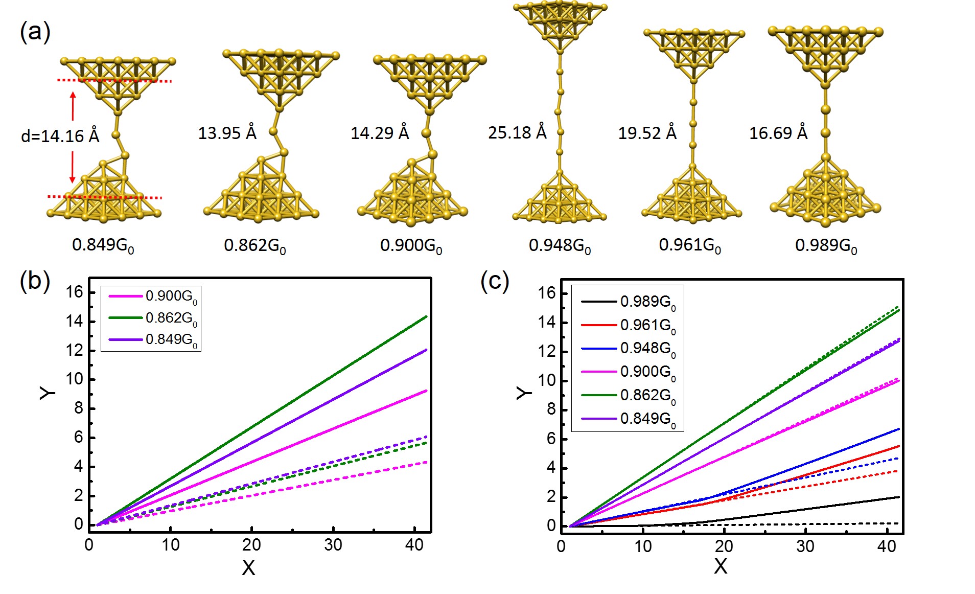
Gold atomic contacts serve as ideal test systems, for which high-quality experimental data of inelastic transport is available Agraït et al. (2002); Kumar et al. (2012). Since transport in atomic-scale junctions is known to depend crucially on the position of individual atoms Agraït et al. (2003), it is important to generate a representative ensemble of atomic junction geometries for a meaningful comparison with experiment. We have therefore set up Au atomic junctions under various strain conditions, exhibiting chains of different lengths at their narrowest cross section. The atomic chains consist of 1 to 7 atoms, as experimentally reported Yanson et al. (1998), and connect two pyramid-shaped Au electrodes in various configurations. The transport direction in the electrodes coincides either with the crystal direction, as shown in Fig. 1, or with the direction, see Fig. 2, since transmission electron microscopy studies have found these crystallographic directions to form in the last stage of the stretching process Rodrigues et al. (2000). We optimize all the atoms in the C region of each junction, which also represents the ”dynamical region”, where atoms can move and vibrations are taken into account. For the first junction of Fig. 1(a) the C region consists of all the atoms, located between the red dotted horizontal lines. In contrast we keep those layers fixed that we attribute to the L and R electrodes. We measure the electrode separation between the first gold layers on each side of the junction that are kept fixed and that are closest to the C region.
Before we consider the full shot noise signal with inelastic contributions, let us discuss differences in the elastic noise for multichannel and single-channel situations. In Fig. 1(b) we study three junctions of Fig. 1(a) with total transmissions of , and . Their four highest eigenchannel transmissions to are specified in Table 1. We find that most of the systems under study exhibit by a single nearly fully transmitting channel. Others contribute with transmissions within the range of 10% of the main channel. If we consider all the channel transmissions in Eq. (2) [solid lines in Fig. 1(b)], we find a higher noise as compared to a hypothetical case of a single channel with [dashed lines in Fig. 1(b)]. This is expected, since the elastic noise decreases monotonically for a single channel with , as approaches 1. For the same reason the noise of the contact with is expected to be below those of the contact with . This ordering is indeed obeyed, if we consider just a single channel. But it is reversed in the multichannel case, since for the particular contact with is lower than for the contact with . This discussion shows that the channels with small transmission can have a significant influence on the shot noise. In this regard single-channel models may miss some interesting physical effects as compared to multichannel ones.
Our full shot noise results for all of the contacts of Fig. 1(a) are shown in Fig. 1(c). By considering different geometrical configurations, we cover a wide range of junction conductances between and . The range of total transmissions is indeed wide enough to observe the transition from a negative to a positive inelastic correction to the noise. Due to the sampling with a limited amount of six geometries, we find the sign crossover to occur between and . We also see that the inelastic signal does not affect the shot noise of the junctions very much that we studied in Fig. 1(b). In particular the counterintuitive ordering of the size of their shot noise signal remains intact. The inelastic signal is larger for the better conducting junctions with , and .
| () | ||||
|---|---|---|---|---|
| 0.900 | 0.836 | |||
| 0.862 | 0.742 | |||
| 0.849 | 0.771 |
In simple terms the EV interaction in multichannel junctions can modify the scattering within a channel or lead to scattering between channels. These two effects may be referred to as intra- and interchannel scattering, respectively. They have been discussed in the literature Bürkle et al. (2013); Wheeler et al. (2013); Ben-Zvi et al. (2013). The theoretical study of Bürkle et al. Bürkle et al. (2013) for the current through an Au chain and the experimental observations of Wheeler et al. Wheeler et al. (2013) for the noise put forward that the sign and magnitude of change at a given voltage due to EV interaction are determined by the transmission of the particular eigenchannel that happens to be strongly coupled to the relevant local vibrational mode in the C part of the many-channel junction. The analysis of inelastic effects in Pt-benzene-Pt and Pt-CO2-Pt molecular junctions with several transmission channels, on the other hand, suggests that the effect of vibrational excitation on conductance can also involve scattering between channels Ben-Zvi et al. (2013).
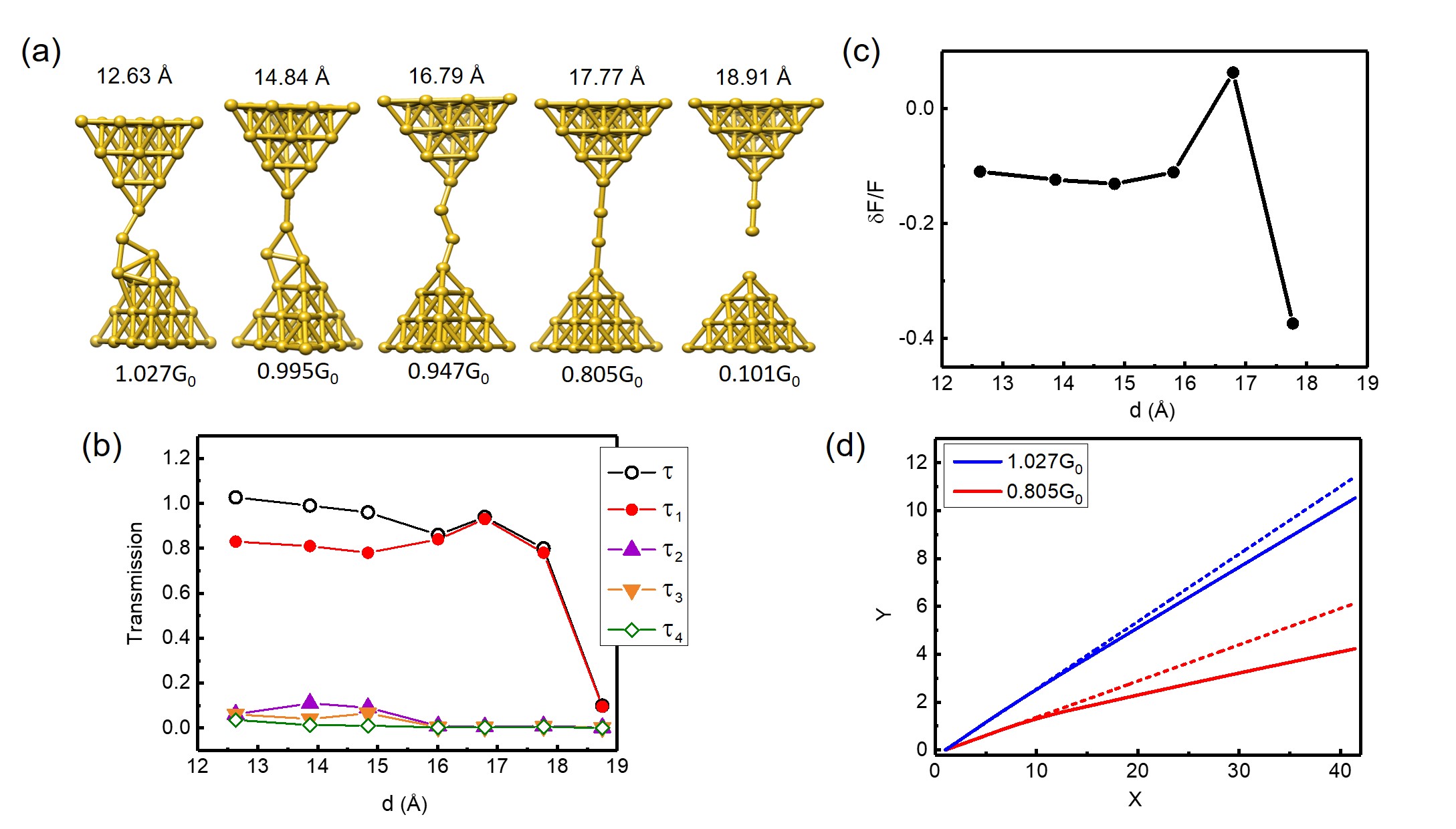
| () | ||||
|---|---|---|---|---|
| 1.027 | 0.835 | |||
| 0.947 | 0.933 | |||
| 0.805 | 0.781 |
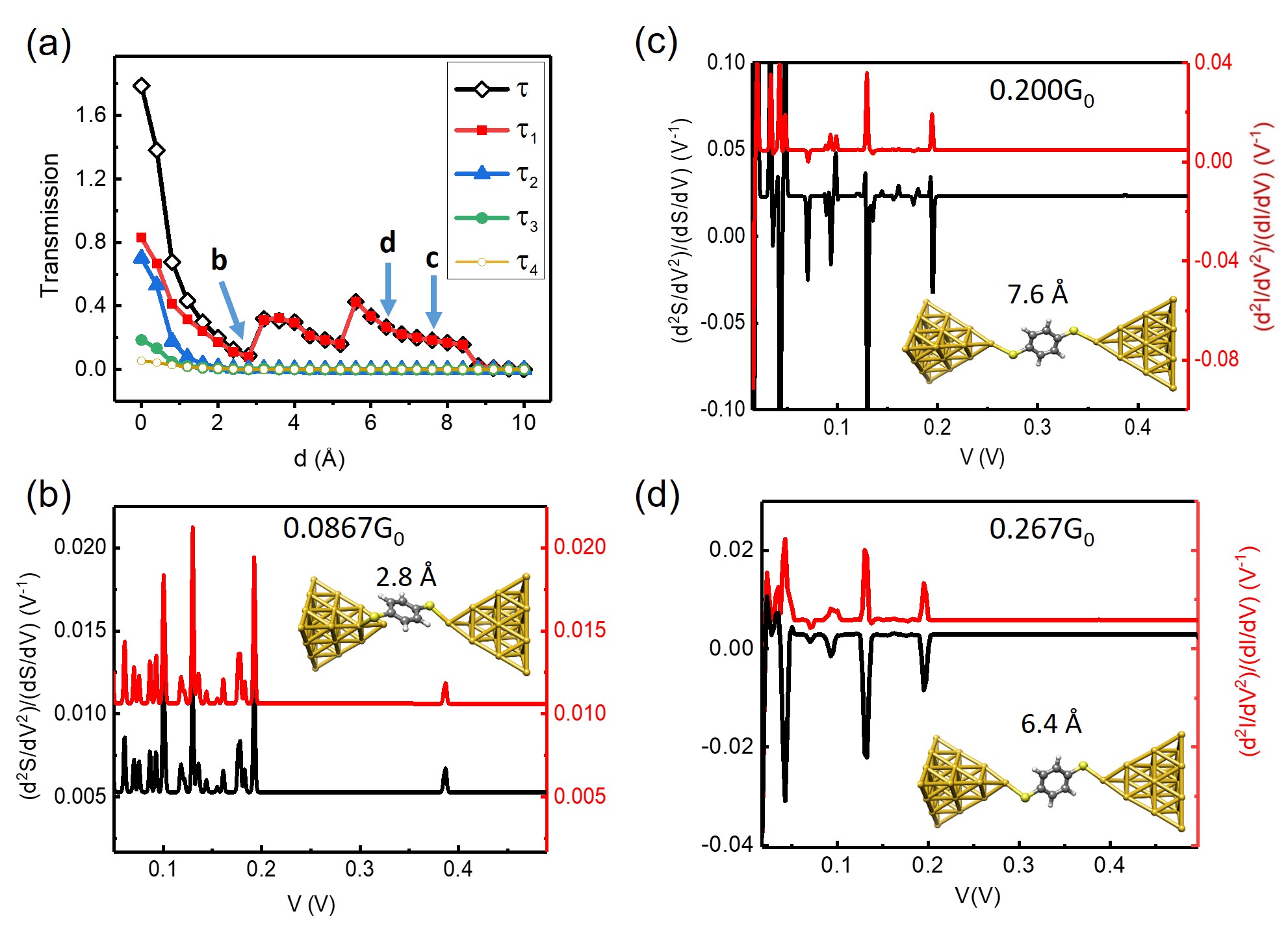
Atomic-scale configurational changes can have considerable effects on the noise, because of the differing numbers of transmission eigenchannels that might be active in each case, the changing symmetry of vibrational modes, and the size of corresponding EV couplings. We study this aspect in Fig. 2 by stretching a junction with electrodes, oriented along the direction. At low interelectrode separations between 12.63 and 14.84 Å, we obtain contacts with as many as four significant transmission eigenchannels, while a single prevalent channel emerges when we continue the stretching. We observe that the sign of the inelastic noise correction in Fig. 2(c) can be well understood by the behavior of the dominant transmission channel , i.e. intrachannel EV coupling. When is below the value of around , the value of is negative, but it changes to positive, when at Å before contact rupture. We specify the transmission values of the highest four channels of the contacts at , and Å in Table 2 and show the - representations of the shot noise for and Å in Fig. 2(d).
As discussed in the introduction, for a symmetric single-channel junction in the SLHM the EV interaction leads to a step up of the conductance for and a step down for , as the energy supplied by the external voltage grows larger than the vibrational energy. In the second derivative of the current with respect to voltage the features appear as a peak or dip, respectively. Along the same line dips are expected at the vibrational activation threshold in the SLHM for the second derivative of the noise with respect to voltage in the interval and peaks in the other regions or . In Fig. 3 we examine these relations for three Au atomic contacts with conductance values of , and by plotting both and , each normalized by the corresponding first derivative.
In contrast to the observations in Ref. Kumar et al. (2012) peaks as well as dips are visible in the IET spectra of Fig. 3. The high-energy part of the spectra is easier to understand than that at low energies. Around 17 to 22 meV, corresponding to the energy range where longitudinal vibrational modes of Au chains occur, we consistently find dips. Despite , the IET signals at low voltage between 5 and 15 mV show a positive sign in Fig. 3(a) and 3(b). In the light of the SLHM this might signal vibrational coupling to eigenchannels with low transmission. Further below, we will see however that this interpretation is incompatible with the behavior of the spectrum. Importantly, as compared to the rather stretched-out geometry in Fig. 3(c), vibrational modes exhibit no clear symmetry in the bent-chain configurations of Fig. 3(a) and 3(b), which may lead to complex EV interaction effects.
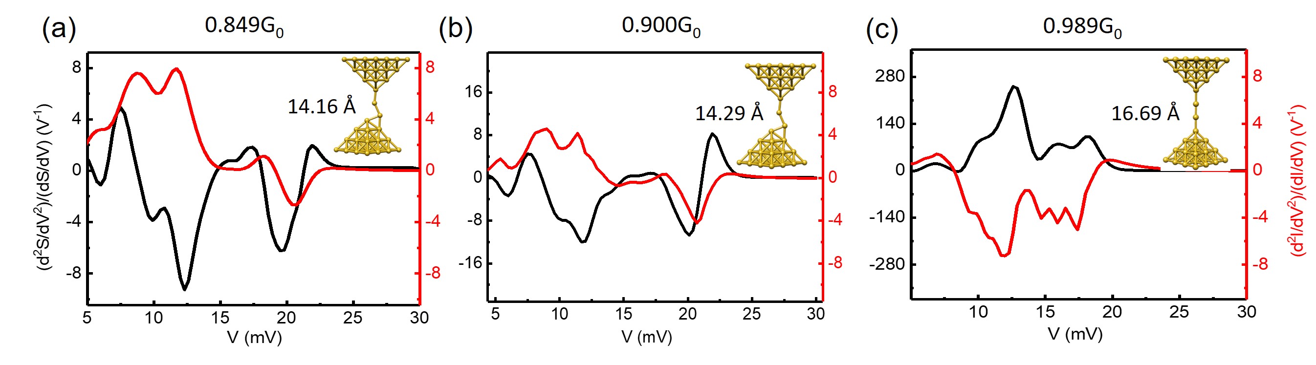
Also the inelastic noise contributions yield a complicated picture. Irrespective of the conductance studied in Fig. 3, features a pronounced voltage dependence. Overall it shows the sign change expected for intrachannel scattering in the SLHM, when considering the size of . As visible from the data in Table 1, for the geometries in Fig. 3(a) and 3(b), and is indeed mainly negative there. For Fig. 3(c) with in contrast it is mostly positive. For that latter contact with and , the signals in and have opposite sign, consistent by the SLHM for this nearly perfect transmission. spectra in Fig. 3(a) and 3(b) show both positive and negative values, which may effectively reduce the integrated signal size of inelastic shot noise corrections. Negative values of between 5 to 15 mV in Fig. 3(a) and 3(b) are inconsistent with vibrational coupling to eigenchannels with , and the role of interchannel mixing needs further exploration. Finally, let us focus on the region around 20 meV, where all of the IET spectra show the expected dip. When going from Fig. 3(a) to 3(c), we reveal a transition from correlation to anticorrelation between and as increases above in agreement with the SLHM. Indeed Fig. 3(b) represents a transitional stage, where is very close to , and displays a dip-peak feature with a corresponding sign change at the peak in the IET spectrum.
III.1.2 Experiment
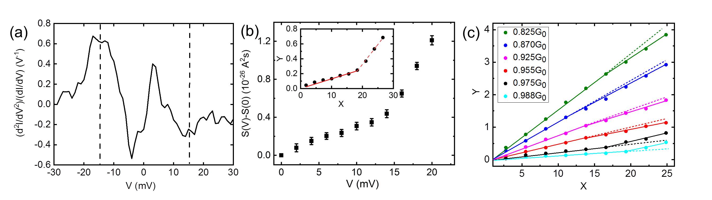
Fig. 4(a) shows the point contact spectrum of an experimentally realized Au atomic contact with a linear conductance of . The prominent dip at mV and corresponding antisymmetric peak at mV indicate an electron scattering process with a vibrational mode. Depending on the atomic configuration, we observe vibrational energies in the range of 10 to 20 meV, which have the tendency to decrease with stretching due to bond softening Agraït et al. (2002). The peak at around 5 mV is usually attributed to a zero-bias anomaly Agraït et al. (2002); Djukic and van Ruitenbeek (2006). But it might also indicate a soft phonon mode Böhler et al. (2007, 2009); Weber and Scheer (2017) and resembles the low-energy features observed in the simulations for the contacts shown in Fig. 3(a) and 3(b).
Fig. 4(b) illustrates the measured current noise of the same contact as a function of bias voltage . The inset displays the corresponding conversion to the reduced quantities and . The red solid line indicates a linear fit up to the voltage, at which significant inelastic excitations set in. The data can be well described by assuming a single channel with a transmission probability of and yields the Fano factor . The dashed line shows the linear fit for voltages above the kink, yielding the modified ”Fano factor” . From these two values we compute the relative change in the Fano factor , as discussed above.
Finally, Fig. 4(c) represents the measured shot noise in the - reduced units for six contacts with conductances from to . The determination of the dominant vibrational mode energy for some of the contacts is difficult due to conductance fluctuations or the mentioned appearance of multiple features in the IET spectra Böhler et al. (2007). We therefore consistently choose the first minimum in the IET spectra at positive voltage as a signature of a vibrational mode and use this voltage for the location of the kink in the - representation of the noise. Solid lines represent the full signal and consist of the two piecewise linear fits to the noise, as described in the previous paragraph.
III.1.3 Comparison between theory and experiment
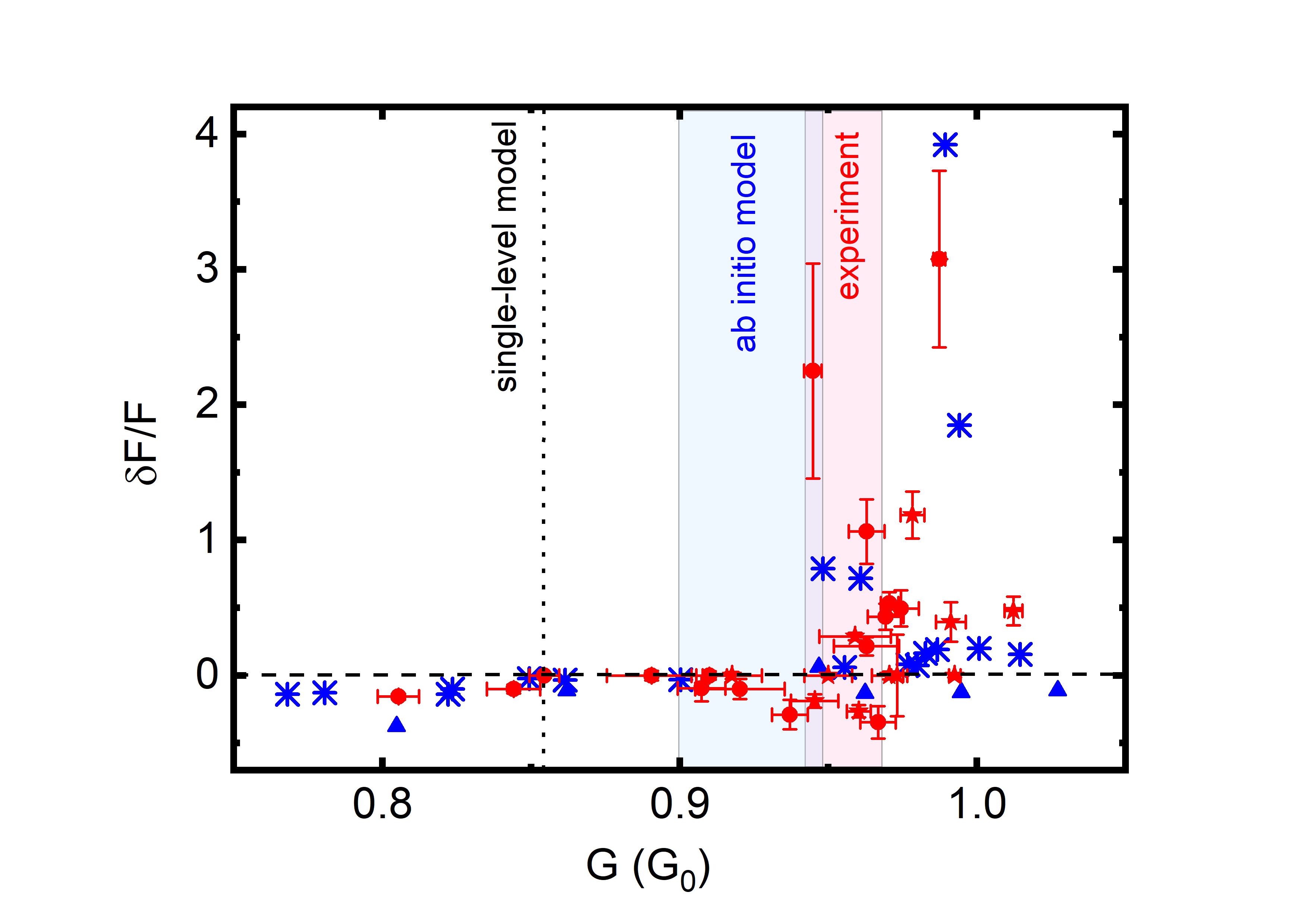
We now compare in detail the results for inelastic shot noise corrections found in theory and in experiment. Fig. 5 shows for 27 measured contacts with conductance values between and . By comparison between actual values and the expectation for the single-channel case, i.e. , we classify the contacts into single-channel and multichannel ones. We assign a single channel, if the contribution of the additional channels to cannot be revealed within our experimental resolution. We cannot assign a sharp numerical criterion here, because this procedure depends on the precision, with which can be measured. The latter is limited by conductance fluctuations or soft phonons, as mentioned above. Taking these considerations into account, the lower limit for transmission contributions of additional channels is on the order of 0.003 to 0.01. Single-channel contacts and multichannel ones are marked with different symbols in Fig. 5. In the same way we plot data from overall 25 theoretically computed contact geometries. Covering the conductance range of to , they split into 19 contacts with leads oriented along the direction and 6 with leads along , which we distinguish by different symbols (see also the corresponding results in Figs. 1 and 2). In the experimental work by Kumar et al. Kumar et al. (2012) the transition from negative to positive was found around . The vertical dotted black line in Fig. 5 represents the value from the symmetrically coupled SLHM of Refs. Avriller and Levy Yeyati (2009); Schmidt and Komnik (2009). In our experimental data we find positive as well as negative in a range between and , shaded in red in Fig. 5, while the bluish area is the prediction of our multichannel and multivibration ab-initio modeling.
Due to the finite amount of calculated junction geometries, our ab-initio model locates the sign crossover in the range between and . Interestingly, our simulations confirm that the threshold is not sharp and provide an explanation for the data points at with negative . As discussed in the context of Figs. 2 and 3, they may arise from multichannel junctions. Also in the experimental data we find a trend of negative values for contacts which we identified as multichannel cases, in agreement with the theoretical findings.
Unlike a previous ab-initio study Avriller and Frederiksen (2012) we are thus able to observe the high-transmission sign change in the inelastic shot noise correction, which was detected experimentally Kumar et al. (2012) and which we confirm here through independent measurements. By considering the electronic multilevel structure and many vibrational modes, the transmission at the sign change is increased from for the SLHM to a value between and , quite compatible with the experiments. At the same time the transition is seen to be washed out by the electronic multilevel structure, since high-conductance junctions can occur with a relatively low transmissive first eigenchannel, which may cause a negative even for . This result is apparent only, since we have explored a large set of junction configurations both in experiment and theory. Our theoretical analysis of in Fig. 3 further demonstrates that positive as well as negative inelastic noise contributions with varying weight may arise in a junction, partially averaging out the integrated inelastic signature in .
Remaining discrepancies between theory and experiment, for instance with respect to the precise position and width of the crossover area, may be attributed to the limited amount of junctions analyzed. The theory might be further improved by going beyond the WBL approximation, in which the energy dependencies of Green’s functions and related quantities are neglected. Furthermore we have concentrated on the symmetric terms of the inelastic noise corrections, as discussed in subsection II.1. From the experimental side, undetected additional noise contributions Lumbroso et al. (2018) or changes of the contacts during the time-consuming noise measurements could affect the determination of the transmissions, and conductance fluctuations superimposed on the vibrationally induced nonlinearities in the point contact spectra might limit the precision of the conductance determination.
III.2 Au-benzenedithiol-Au contacts
So far the effect of EV interactions on the noise characteristics of molecular contacts is scarcely studied. The majority of shot noise measurements for single-molecule junctions was carried out at low bias voltages, and they use to extract information on elastic transmission coefficients, as mentioned above Djukic and van Ruitenbeek (2006); Kiguchi et al. (2008); Ben-Zvi et al. (2013); Karimi et al. (2016a). Only very recently the inelastic contributions to shot noise have been addressed experimentally in these kind of systems Tewari et al. (2019). However, Ref. Tewari et al. (2019) concentrated on highly transmissive contacts with a conductance close to . BDT contacted by Au electrodes has been demonstrated to be a system with widely tunable conductance values from to more than Kim et al. (2011). Beside inelastic current contributions Kim et al. (2011) some of the authors reported measurements of the elastic noise in this system Karimi et al. (2016a), covering a similar conductance range between and . The adjustment of the conductance by mechanical control should allow experimental access to the transition from positive to negative inelastic shot noise corrections in the low-conductance regime near , as we will show theoretically in the following.
We use here the geometries that we have determined in Ref. Karimi et al. (2016a) during the stretching of a Au-BDT-Au junction to evaluate the inelastic noise. Similar to the gold junctions we analyze in Fig. 6 the appearance of peaks and dips in the second voltage derivative of current and noise. For this purpose we select three different junction configurations with , and , whose transmission coefficients to are specified in Table 3. The progression of the total transmission and those of the largest four eigenchannels is shown in Fig. 6(a) as the separation between the electrodes increases. In this case the distance specifies the displacement of the electrodes with respect to the starting geometry. Since the transmission of the selected geometries remains below , we expect that the IET spectra show mainly peaks, while should exhibit a transition from peaks to dips as the conductance increases. This behavior is exactly seen, when going from the low conductance of in Fig. 6(b) via the intermediate case at with peaks and dips in in Fig. 6(c) to in Fig. 6(d). More generally, Fig. 6 shows that spikes in and correlate in an excellent manner. In addition, we note that both and show a certain offset from zero at finite voltages in Fig. 6(a) to 6(d). It stems from a quadratic background due to phonon heating Viljas et al. (2005); Bürkle et al. (2013), as will be discussed further in subsection III.3.
Our results for the different Au-BDT-Au junction geometries show that the change in the noise from positive to negative inelastic corrections in the low-conductance regime occurs slightly above the value , predicted by the SLHM. As shows both positive and negative values for , we attribute the increased threshold conductance to the complex interplay between multiple electronic and vibrational levels coupled via the EV interaction, in analogy to the results for pure Au contacts.
III.3 Heating at high bias voltages
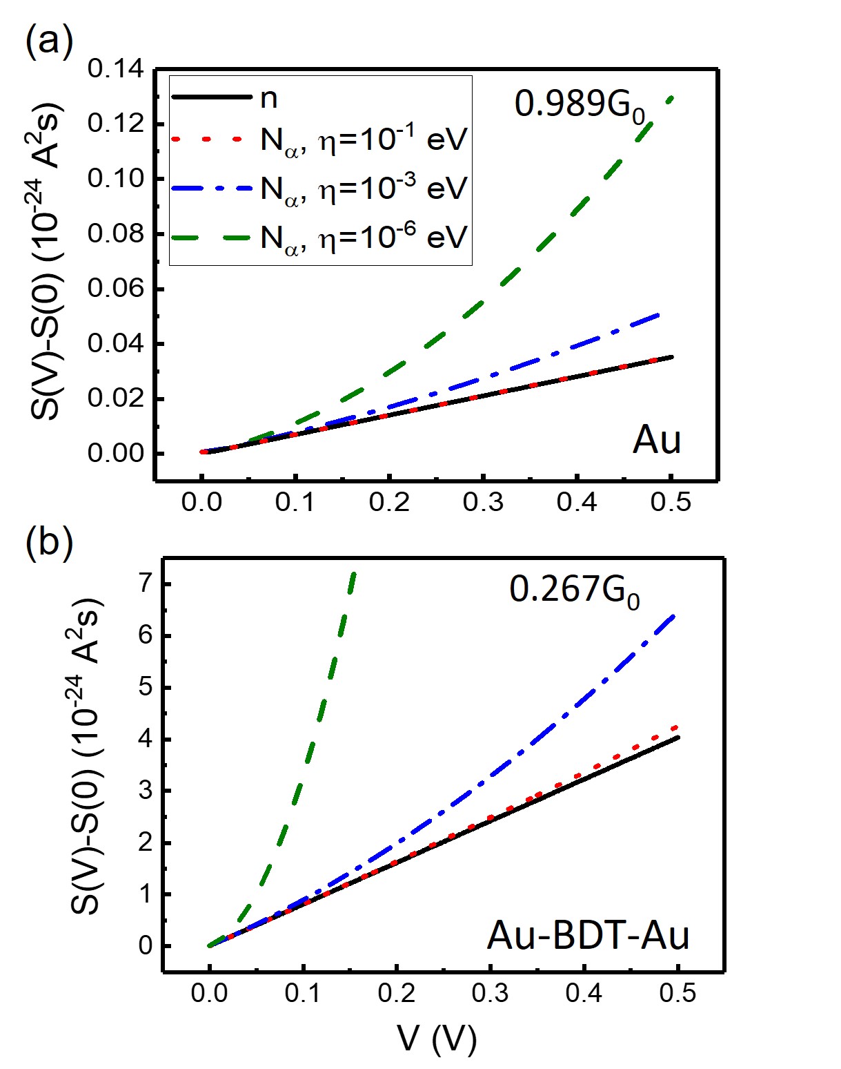
At high bias voltages a nonequilibrium phonon population will be excited in atomic and molecular junctions. Theoretical calculations predict the noise in this regime to grow as with due to the coupling between electrons and thermally nonequilibrated vibrational modes Haupt et al. (2010); Urban et al. (2010); Novotný et al. (2011); Novotný and Belzig (2015).
As we presented before, we include the effects of vibrational heating on inelastic noise by considering the nonequilibrium vibrational occupation in Eq. (11). The vibrational broadening describes the coupling of the vibrational modes to an external reservoir, as provided by the electrodes, and the related damping. It is the only free parameter in our theoretical model. Based on the favorable comparison of theoretical IET spectra Viljas et al. (2005) to high-quality experimental data for Au atomic-chain junctions Agraït et al. (2002), we believe that our default parameter of eV is a realistic value. Nonetheless, in Fig. 7 we show for Au and Au-BDT-Au junctions with conductances of and , respectively, how the shot noise varies with at high bias. For large enough , Eq. (11) reduces to the equilibrium Bose distribution, and the shot noise increases linearly with voltage. If is reduced sufficiently, however, we find a superlinear noise curve that can be fitted by a linear plus a quadratic term.
The fact that we can explain the experimental data for Au atomic junctions in Fig. 4(c) by piecewise linear fits means that there is no significant influence of thermally nonequilibrated vibrational modes on at the low biases measured. A quadratic increase in shot noise, reminiscent of the theoretical predictions with low , has however been observed experimentally at room temperature for a junction conductance of and for applied voltages up to around V Chen et al. (2014). Subsequent studies at low temperatures between 4.2 and 100 K rather emphasize the fact that EV interactions and heating of phonons in atomic contacts are weak Chen and Natelson (2016). Our results confirm these experimental studies.
IV Conclusions
In summary, based on the NEGF technique and using a Hamiltonian parameterized from DFT, we have studied inelastic effects due to EV coupling on the current noise in systems with multiple electronic levels and vibrational modes. Sign crossover thresholds for inelastic noise are observed at conductances of and - for Au-BDT-Au single-molecule and pure Au single-atom contacts, respectively. As compared to the SLHM that predicts values of and , respectively, this increase can be understood by the presence of several partially open transmission eigenchannels that contribute to the total transmission in addition to a dominant one and couple differently to various vibrations. In other words since the inelastic signals are mainly determined by the highest conduction channel and since the transmission of the dominant channel is always lower than the total transmission , the apparent inelastic sign thresholds are shifted towards higher than expected from the simplified single-level toy model.
We have also reported shot noise measurements for Au contacts, using the mechanically controllable break-junction technique and applying a custom-made, versatile setup with simplified measurement electronics Karimi et al. (2016a). The measurements show nonlinearities in the shot noise power for bias voltages around corresponding characteristic vibrational mode energies. The observed crossover from positive to negative sign of inelastic shot noise corrections, as quantified by the relative Fano factor , occurs in a range between and . Our findings confirm previous experimental results Kumar et al. (2012), in which the crossover was located at . We conclude that the deviation between the analytically predicted crossover at for a single channel and the experimental observation for Au contacts may be explained by the occurrence of multichannel contacts in the experiment. Multiple transmissive eigenchannels also provide a natural explanation for why the transition is not sharp. Indeed we find negative values of for both in experiment and theory, which can be assigned to contacts with increased transmission values for channels .
Finally, we have theoretically explored the effects of vibrational heating on the current noise properties as a function of the coupling of vibrations to an external reservoir in the electrodes. For low enough coupling we find a quadratic increase of the noise as a function of voltage at large bias. With increasing coupling the bias-dependent noise becomes linear as the nonequilibrium distribution approaches the equilibrium one. This behavior is similar both for Au single-atom and Au-BDT-Au single-molecule junctions.
The inelastic sign crossover in the noise at low conductance values could not be measured yet and thus remains to be verified. The challenging experiments employing high bias voltages are expected to reveal important insights into charge transport through nanosystems beyond elastic theories.
V Acknowledgments
We thank Juan Carlos Cuevas for stimulating discussions and Federica Haupt for scientific exchange. All authors acknowledge financial support through the Collaborative Research Center (SFB) 767 of the German Research Foundation (DFG). In addition F.P. thanks the Carl Zeiss Foundation for funding. An important part of the numerical modeling was carried out on the computational resources of the bwHPC program, namely the bwUniCluster and the JUSTUS HPC facility.
References
- Blanter and Büttiker (2000) Ya. M. Blanter and M. Büttiker, “Shot noise in mesoscopic conductors,” Phys. Rep. 336, 1 (2000).
- Beenakker and Schönenberger (2003) C. Beenakker and C. Schönenberger, “Quantum shot noise,” Phys. Today 56, 37–42 (2003).
- Cuevas and Scheer (2017) J. C. Cuevas and E. Scheer, Molecular Electronics (World Scientific, Singapore, 2017).
- de Picciotto et al. (1997) R. de Picciotto, M. Reznikov, M. Heiblum, V. Umansky, G. Bunin, and D. Mahalu, “Direct observation of a fractional charge,” Nature 389, 162 (1997).
- Saminadayar et al. (1997) L. Saminadayar, D. C. Glattli, Y. Jin, and B. Etienne, “Observation of the fractionally charged Laughlin quasiparticles,” Phys. Rev. Lett. 79, 2526 (1997).
- Cron et al. (2001) R. Cron, M. F. Goffman, D. Esteve, and C. Urbina, “Multiple-charge-quanta shot noise in superconducting atomic contacts,” Phys. Rev. Lett. 86, 4104 (2001).
- Zhou et al. (2019) P. Zhou, L. Chen, Y. Liu, I. Sochnikov, A. T. Bollinger, M.-G. Han, Y. Zhu, X. He, I. Bozǒvić, and D. Natelson, “Electron pairing in the pseudogap state revealed by shot noise in copper oxide junctions,” Nature 572, 493 (2019).
- Lumbroso et al. (2018) O. S. Lumbroso, L. Simine, A. Nitzan, D. Segal, and O. Tal, “Electronic noise due to temperature differences in atomic-scale junctions,” Nature 562, 240 (2018).
- Reznikov et al. (1995) M. Reznikov, M. Heiblum, H. Shtrikman, and D. Mahalu, “Temporal correlation of electrons: Suppression of shot noise in a ballistic quantum point contact,” Phys. Rev. Lett. 75, 3340 (1995).
- van den Brom and van Ruitenbeek (1999) H. E. van den Brom and J. M. van Ruitenbeek, “Quantum suppression of shot noise in atom-size metallic contacts,” Phys. Rev. Lett. 82, 1526 (1999).
- Djukic and van Ruitenbeek (2006) D. Djukic and J. M. van Ruitenbeek, “Shot noise measurements on a single molecule,” Nano Lett. 6, 789 (2006).
- Kiguchi et al. (2008) M. Kiguchi, O. Tal, S. Wohlthat, F. Pauly, M. Krieger, D. Djukic, J. C. Cuevas, and J. M. van Ruitenbeek, “Highly conductive molecular junctions based on direct binding of benzene to platinum electrodes,” Phys. Rev. Lett. 101, 046801 (2008).
- Schneider et al. (2010) N. L. Schneider, G. Schull, and R. Berndt, “Optical probe of quantum shot-noise reduction at a single-atom contact,” Phys. Rev. Lett. 105, 026601 (2010).
- Schneider et al. (2012) N. L. Schneider, L. T. Lü, M. Brandbyge, and R. Berndt, “Light emission probing quantum shot noise and charge fluctuations at a biased molecular junction,” Phys. Rev. Lett. 109, 186601 (2012).
- Kumar et al. (2013) M. Kumar, O. Tal, R. H. M. Smit, A. Smogunov, E. Tosatti, and J. M. van Ruitenbeek, “Shot noise and magnetism of Pt atomic chains: Accumulation of points at the boundary,” Phys. Rev. B 88, 245431 (2013).
- Ben-Zvi et al. (2013) R. Ben-Zvi, R. Vardimon, T. Yelin, and O. Tal, “Electron-vibration interaction in multichannel single-molecule junctions,” ACS Nano 7, 11147 (2013).
- Vardimon et al. (2013) R. Vardimon, M. Klionsky, and O. Tal, “Experimental determination of conduction channels in atomic-scale conductors based on shot noise measurements,” Phys. Rev. B 88, 161404 (2013).
- Karimi et al. (2016a) M. A. Karimi, S. G. Bahoosh, M. Herz, R. Hayakawa, F. Pauly, and E. Scheer, “Shot noise of 1,4-benzenedithiol single-molecule junctions,” Nano Lett. 16, 1803 (2016a).
- Sánta et al. (2019) B. Sánta, Z. Balogh, A. Gubicza, L. Pósa, D. Krisztián, G. Mihály, M. Csontos, and A. Halbritter, “Universal type current noise of Ag filaments in redox-based memristive nanojunctions,” Nanoscale 11, 4719 (2019).
- Xiang et al. (2015) D. Xiang, V. Sydoruk, S. Vitusevich, M. V. Petrychuk, A. Offenhäusser, V. A. Kochelap, A. E. Belyaev, and D. Mayer, “Noise characterization of metal-single molecule contacts,” Appl. Phys. Lett. 106, 063702 (2015).
- Büttiker (1992) M. Büttiker, “Scattering theory of current and intensity noise correlations in conductors and wave guides,” Phys. Rev. B 46, 12485 (1992).
- Agraït et al. (2003) N. Agraït, A. Levy Yeyati, and J. M. van Ruitenbeek, “Quantum properties of atomic-sized conductors,” Phys. Rep. 377, 81 (2003).
- Song and Lee (2017) Y. Song and T. Lee, “Electronic noise analyses on organicelectronic devices,” J. Mat. Chem. C 5, 7123 (2017).
- (24) F. Evers, R. Korytár, S. Tewari, and J. M. van Ruitenbeek, “Advances and challenges in single-molecule electron transport,” arXiv:1906.10449 .
- Agraït et al. (2002) N. Agraït, C. Untiedt, G. Rubio-Bollinger, and S. Vieira, “Onset of energy dissipation in ballistic atomic wires,” Phys. Rev. Lett. 88, 216803 (2002).
- Smit et al. (2002) R. H. M. Smit, Y. Noat, C. Untiedt, N. D. Lang, M. C. van Hemert, and J. M. van Ruitenbeek, “Measurement of the conductance of a hydrogen molecule,” Nature 419, 906 (2002).
- Kushmerick et al. (2004) J. G. Kushmerick, J. Lazorcik, C. H. Patterson, R. Shashidhar, D. S. Seferos, and G. C. Bazan, “Vibronic contributions to charge transport across molecular junctions,” Nano Lett. 4, 639 (2004).
- Wang et al. (2004) W. Wang, T. Lee, I. Kretzschmar, and M. A. Reed, “Inelastic electron tunneling spectroscopy of an alkanedithiol self-assembled monolayer,” Nano Lett. 4, 643 (2004).
- Galperin et al. (2004) M. Galperin, M. A. Ratner, and A. Nitzan, “Inelastic electron tunneling spectroscopy in molecular junctions: Peaks and dips,” J. Chem. Phys. 121, 11965 (2004).
- Song et al. (2009) H. Song, Y. Kim, Y. H. Jang, H. Jeong, M. A. Reed, and T. Lee, “Observation of molecular orbital gating,” Nature 462, 1039 (2009).
- Kim et al. (2011) Y. Kim, T. Pietsch, A. Erbe, W. Belzig, and E. Scheer, “Benzenedithiol: A broad-range single-channel molecular conductor,” Nano Lett. 11, 3734 (2011).
- Karimi et al. (2016b) M. A. Karimi, S. G. Bahoosh, M. Valášek, M. Bürkle, M. Mayor, F. Pauly, and E. Scheer, “Identification of the current path for a conductive molecular wire on a tripodal platform,” Nanoscale 8, 10582 (2016b).
- Ioffe et al. (2008) Z. Ioffe, T. Shamai, A. Ophir, G. Noy, I. Yutsis, K. Kfir, O. Cheshnovsky, and Y. Selzer, “Detection of heating in current-carrying molecular junctions by Raman scattering,” Nat. Nanotechnol. 3, 727 (2008).
- Ward et al. (2010) D. R. Ward, D. A. Corley, J. M. Tour, and D. Natelson, “Vibrational and electronic heating in nanoscale junctions,” Nat. Nanotechnol. 6, 33 (2010).
- Bi et al. (2018) H. Bi, C.-A. Palma, Y. Gong, P. Hasch, M. Elbing, M. Mayor, J. Reichert, and J. V. Barth, “Voltage-driven conformational switching with distinct Raman signature in a single-molecule junction,” J. Am. Chem. Soc. 140, 4835 (2018).
- de la Vega et al. (2006) L. de la Vega, A. Martín-Rodero, N. Agraït, and A. Levy Yeyati, “Universal features of electron-phonon interactions in atomic wires,” Phys. Rev. B 73, 075428 (2006).
- Paulsson et al. (2005) M. Paulsson, T. Frederiksen, and M. Brandbyge, “Modeling inelastic phonon scattering in atomic- and molecular-wire junctions,” Phys. Rev. B 72, 201101 (2005).
- Paulsson et al. (2008) M. Paulsson, T. Frederiksen, H. Ueba, N. Lorente, and M. Brandbyge, “Unified description of inelastic propensity rules for electron transport through nanoscale junctions,” Phys. Rev. Lett. 100, 226604 (2008).
- Schinabeck et al. (2016) C. Schinabeck, A. Erpenbeck, R. Härtle, and M. Thoss, “Hierarchical quantum master equation approach to electronic-vibrational coupling in nonequilibrium transport through nanosystems,” Phys. Rev. B 94, 201407 (2016).
- Frederiksen et al. (2007) T. Frederiksen, M. Paulsson, M. Brandbyge, and A.-P. Jauho, “Inelastic transport theory from first principles: Methodology and application to nanoscale devices,” Phys. Rev. B 75, 205413 (2007).
- Bürkle et al. (2013) M. Bürkle, J. K. Viljas, T. J. Hellmuth, E. Scheer, F. Weigend, G. Schön, and F. Pauly, “Influence of vibrations on electron transport through nanoscale contacts,” Phys. Status Solidi B 250, 2468 (2013).
- Tal et al. (2008) O. Tal, M. Krieger, B. Leerink, and J. M. van Ruitenbeek, “Electron-vibration interaction in single-molecule junctions: From contact to tunneling regimes,” Phys. Rev. Lett. 100, 196804 (2008).
- Avriller and Levy Yeyati (2009) R. Avriller and A. Levy Yeyati, “Electron-phonon interaction and full counting statistics in molecular junctions,” Phys. Rev. B 80, 041309 (2009).
- Schmidt and Komnik (2009) T. L. Schmidt and A. Komnik, “Charge transfer statistics of a molecular quantum dot with a vibrational degree of freedom,” Phys. Rev. B 80, 041307 (2009).
- Haupt et al. (2009) F. Haupt, T. Novotný, and W. Belzig, “Phonon-assisted current noise in molecular junctions,” Phys. Rev. Lett. 103, 136601 (2009).
- Kim (2014) S. Kim, “Inelastic current noise in nanoscale systems: Scattering theory analysis,” Phys. Rev. B 89, 035413 (2014).
- Haupt et al. (2010) F. Haupt, T. Novotný, and W. Belzig, “Current noise in molecular junctions: Effects of the electron-phonon interaction,” Phys. Rev. B 82, 165441 (2010).
- Avriller and Frederiksen (2012) R. Avriller and T. Frederiksen, “Inelastic shot noise characteristics of nanoscale junctions from first principles,” Phys. Rev. B 86, 155411 (2012).
- Novotný et al. (2011) T. Novotný, F. Haupt, and W. Belzig, “Nonequilibrium phonon backaction on the current noise in atomic-sized junctions,” Phys. Rev. B 84, 113107 (2011).
- Novotný and Belzig (2015) T. Novotný and W. Belzig, “Large-voltage behavior of charge transport characteristics in nanosystems with weak electron-vibration coupling,” Beilstein J. Nanotechnol. 6, 1853 (2015).
- Tsutsui et al. (2010) M. Tsutsui, M. Taniguchi, and T. Kawai, “Single-molecule identification via electric current noise,” Nat. Commun. 1, 138 (2010).
- Kumar et al. (2012) M. Kumar, R. Avriller, A. Levy Yeyati, and J. M. van Ruitenbeek, “Detection of vibration-mode scattering in electronic shot noise,” Phys. Rev. Lett. 108, 146602 (2012).
- Chen et al. (2014) R. Chen, P. J. Wheeler, M. Di Ventra, and D. Natelson, “Enhanced noise at high bias in atomic-scale Au break junctions,” Sci. Rep. 4, 4221 (2014).
- Chen and Natelson (2016) R. Chen and D. Natelson, “Evolution of shot noise in suspended lithographic gold break junctions with bias and temperature,” Nanotechnology 27, 245201 (2016).
- Tewari and van Ruitenbeek (2018) S. Tewari and J. van Ruitenbeek, “Anomalous nonlinear shot noise at high voltage bias,” Nano Lett. 18, 5217 (2018).
- Tewari et al. (2019) S. Tewari, C. Sabater, and J. van Ruitenbeek, “Identification of vibration modes in single-molecule junctions by strong inelastic signals in noise,” Nanoscale 11, 19462 (2019).
- Viljas et al. (2005) J. K. Viljas, J. C. Cuevas, F. Pauly, and M. Häfner, “Electron-vibration interaction in transport through atomic gold wires,” Phys. Rev. B 72, 245415 (2005).
- Urban et al. (2010) D. F. Urban, R. Avriller, and A. Levy Yeyati, “Nonlinear effects of phonon fluctuations on transport through nanoscale junctions,” Phys. Rev. B 82, 121414 (2010).
- Pauly et al. (2008) F. Pauly, J. K. Viljas, U. Huniar, M. Häfner, S. Wohlthat, M. Bürkle, J. C. Cuevas, and G. Schön, “Cluster-based density-functional approach to quantum transport through molecular and atomic contacts,” New J. Phys. 10, 125019 (2008).
- (60) TURBOMOLE, https://www.turbomole.org .
- Dirac (1929) P. A. M. Dirac, “Quantum mechanics of many-electron systems,” Proc. R. Soc. London, Ser. A 123, 714 (1929).
- Perdew et al. (1996) J. P. Perdew, K. Burke, and Y. Wang, “Generalized gradient approximation for the exchange-correlation hole of a many-electron system,” Phys. Rev. B 54, 16533 (1996).
- Perdew and Wang (1992) J. P. Perdew and Y. Wang, “Accurate and simple analytic representation of the electron-gas correlation energy,” Phys. Rev. B 45, 13244 (1992).
- Slater (1951) J. C. Slater, “A simplification of the Hartree-Fock method,” Phys. Rev. 81, 385 (1951).
- Schäfer et al. (1992) A. Schäfer, H. Horn, and R. Ahlrichs, “Fully optimized contracted Gaussian basis sets for atoms Li to Kr,” J. Chem. Phys. 97, 2571 (1992).
- Eichkorn et al. (1995) K. Eichkorn, O. Treutler, H. Öhm, M. Häser, and R. Ahlrichs, “Auxiliary basis sets to approximate Coulomb potentials,” Chem. Phys. Lett. 240, 283 (1995).
- Eichkorn et al. (1997) K. Eichkorn, F. Weigend, O. Treutler, and R. Ahlrichs, “Auxiliary basis sets for main row atoms and transition metals and their use to approximate Coulomb potentials,” Theor. Chem. Acc. 97, 119 (1997).
- Scheer et al. (2001) E. Scheer, W. Belzig, Y. Naveh, M. H. Devoret, D. Esteve, and C. Urbina, “Proximity effect and multiple Andreev reflections in gold atomic contacts,” Phys. Rev. Lett. 86, 284 (2001).
- Yanson et al. (1998) A. I. Yanson, G. Rubio Bollinger, H. E. van den Brom, N. Agraït, and J. M. van Ruitenbeek, “Formation and manipulation of a metallic wire of single gold atoms,” Nature 395, 783 (1998).
- Rodrigues et al. (2000) V. Rodrigues, T. Fuhrer, and D. Ugarte, “Signature of atomic structure in the quantum conductance of gold nanowires,” Phys. Rev. Lett. 85, 4124 (2000).
- Wheeler et al. (2013) P. J. Wheeler, R. Chen, and D. Natelson, “Noise in electromigrated nanojunctions,” Phys. Rev. B 87, 155411 (2013).
- Böhler et al. (2007) T. Böhler, A. Edtbauer, and E. Scheer, “Conductance of individual molecules measured with controllable gold electrodes,” Phys. Rev. B 76, 125432 (2007).
- Böhler et al. (2009) T. Böhler, A. Edtbauer, and E. Scheer, “Point-contact spectroscopy on aluminium atomic-size contacts: longitudinal and transverse vibronic excitations,” New J. Phys. 11, 013036 (2009).
- Weber and Scheer (2017) D. Weber and E. Scheer, “Superconducting properties of lithographic lead break junctions,” Nanotechnology 29, 045703 (2017).