Transport in armchair graphene nanoribbons and in ordinary waveguides
Abstract
We study dc and ac transport along armchair graphene nanoribbons using the spectrum and eigenfunctions and general linear-response expressions for the conductivities. Then we contrast the results with those for transport along ordinary waveguides. In all cases we assess the influence of elastic scattering by impurities, describe it quantitatively with a Drude-type contribution to the current previously not reported, and evaluate the corresponding relaxation time for long- and short-range impurity potentials. We show that this contribution dominates the response at very low frequencies. In both cases the conductivities increase with the electron density and show cusps when new subbands start being occupied. As functions of the frequency the conductivities in armchair graphene nanoribbons exhibit a much richer peak structure than in ordinary waveguides: in the former intraband and interband transitions are allowed whereas in the latter only the intraband ones occur. This difference can be traced to that between the corresponding spectra and eigenfunctions.
I Introduction
Graphene nanoribbons have been studied extensively theoretically and experimentally. Previous studies focused on their electronic structure, spectrum, and eigenfunctions [1], optical properties [2; 3], elementary excitations [4], magnetic susceptibility [5; 6], excitonic effects [7]. A short review of transport properties, focused on localization concepts, appeared in Ref. [8], some numerical results in Ref. [9], numerically studied thermal transport in Ref. [10], and spin tranport in substitutionally doped, zig-zag graphene nanoribbons in Ref. [11]. Experimental results have also been reported [12]. The influence of impurity scattering or disorder though has received a limited attention [11]. In particular, we are not aware of any study of dc and ac transport, say, within linear-response theory, that takes into account scattering by randomly distributed impurities, most of the studies use scattering-independent Kubo formulas or consider scattering numerically.
In this work we study dc and ac transport along armchair graphene nanoribbons (AGNRs) or ordinary waveguides using linear-response, scattering-dependent and scattering-independent expressions for the conductivities. In the former case we evaluate the relaxation time for long- and short-range impurity potentials. We present the basics in Sec. II and the conductivities in Sec. III. A summary follows in Sec. IV.
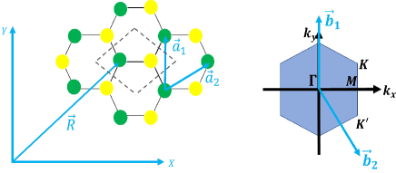
its primitive vectors and . Right panel: The corresponding Brillouin zone with and the reciprocal lattice vectors.
II AGNRs, ordinary waveguides
II.1 AGNRs
Graphene is a two-dimensional, one-atom thick planar sheet of bonded carbon atoms densely packed in a honeycomb structure as shown in the left panel of Fig. 1. In it the ribbon extends along the axis while the graphene sheet is confined along the axis. The lattice structure can be viewed as a triangular lattice with two sites (green filled circles) and (yellow filled circles) per unit cell as shown by the rectangular box in the left panel of Fig. 1. The arrows indicate the primitive lattice vectors and , with the triangular lattice constant of the structure, and span the graphene lattice. Further, and generate the reciprocal lattice vectors of the Brillouin zone, cf. Fig. 1, given by and . From the explicit expressions of and we find the two inequivalent Dirac points (valleys) given by and . The Hamiltonian near the Dirac points reads
| (1) |
where is Plank’s constant, the Fermi velocity, and . The resulting eigenfunctions of Eq. (1) for AGNRs, shown in Fig. 2, take the form

| (2) |
where . The energy dispersion of graphene AGNRs corresponding to Eq. (1) is [1]
| (3) |
where stands for the conduction (valence) band. The allowed values of are [1; 2; 4; 5]
| (4) |
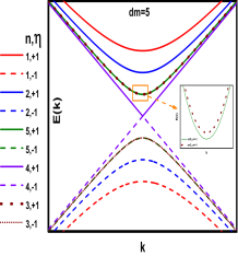
here is the ribbon width, the number of rows of AGNRs, , is the carbon-carbon distance, and is the subband index with the maximum number of dimmers. It follows from Eq. (4), if , then for particular . So, a zero energy state appears near as in graphene, whereas the other states have band gap because . The energy dispersions for semiconducting and metallic nanoribbons are shown in Fig. 3.

Velocity matrix elements. To evaluate the various conductivities we need the matrix elements of the velocity operators and . With
| (5) |
their matrix elements () are
| (6) | |||
| (7) |
with , , and .
II.2 Ordinary waveguides
In Fig. 4 we consider an ordinary quantum wire along the axis generated by confining a 2DEG along the direction. We assume the confining potential to be parabolic, i.e., . The eigenvalues are
| (8) |
and the corresponding eigenfunctions
| (9) |
with and the Hermite polynomials. Here only the diagonal matrix elements are relevant since the nondiagonal ones () vanish. However, the nondiagonal velocity matrix elements () along the confinement direction are non zero and given as
| (10) |
where . It is evident from the right panel of Fig. 4 that the spectrum consists of a set of equidistant, oscillator subbands due to the harmonic confinement along the direction.
III Conductivities
We consider a many-body system described by the Hamiltonian , where is the unperturbed part, is a binary-type interaction (e.g., between electrons and impurities or phonons), and is the interaction of the system with the external field F(t) [13]. For conductivity problems we have , where is the electric field, the electron charge, , and the position operator of electron . In the representation in which is diagonal the many-body density operator has a diagonal part and a nondiagonal part . For weak electric fields and weak scattering potentials, for which the first Born approximation applies, the conductivity tensor has a diagonal part and a nondiagonal part ; the total conductivity is .
In general we have two kinds of currents, diffusive and hopping, with , but usually only one of them is present. If no magnetic field is present, the hop-
ping term vanishes identically [13] and only the term survives. For elastic scattering it is given by [13; 14]


| (11) |
where is the momentum relaxation time, the frequency, and the diagonal matrix elements of the velocity operator. Further, is the Fermi-Dirac distribution function, , the temperature, the Boltzmann constant, and the area of the sample.
Regarding the contribution one can use the identity and cast the original form in the more familiar one [13; 14]
| (12) |
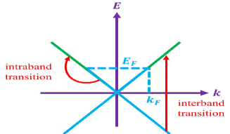
where the sum runs over all quantum numbers and with . The infinitesimal quantity in the original form [13] has been replaced by to account for the broadening of the energy levels. In Eq. (12) and are the nondiagonal matrix elements of the velocity operator. Further, diagonal and nondiagonal contributions describe intraband and interband transitions, respectively, as shown schematically in Fig. 5.
III.1 Diagonal conductivity in ordinary waveguides
For and Eq. (11) becomes
| (13) |
For very low temperatures, we make the approximation , replace by , and use the prescription . Then Eq. (13), with , takes the form
| (14) |
where and . For the dc conductivity we simply set .
In Fig. 6 we show the diagonal conductivity as a function of (upper panel) and photon energy (lower panel) for meV [15]. The conductivity increases with the increase of but cusps appear due to the presence of discrete levels in the lateral direction produced by the parabolic confinement. In addition, vanishes when the Fermi level is in the range since the electron density is null in this range of energy. We can see that has a Drude-type peak around while has peak around as can be seen in the lower panel of Fig. 6. Furthermore, it can also be seen that the Drude-type contribution survives at low frequencies while it vanishes at higher frequencies. Note that the nondiagonal contribution to the conductivity of 2DEG when confined in a ribbon vanishes, since the velocity matrix elements are diagonal, whereas we will find below that it survives in graphene ribbons.
III.2 Nondiagonal conductivity in ordinary waveguides
With the help of matrix elements (10) and , we can recast Eq. (12) as
| (15) | |||||
where . In the limit , one can show that vanishes.
In Fig. 6 (b), we have plotted the numerically evaluated (dark green curve) and (red dotted curve) as functions of the dimensionless photon energy . We can see that is finite at , due to , and attains a maximum value at . Upon further increasing we see that approaches to zero. On the other hand, we observe that acquires positive and negative values due to the factor in Eq. (15). For , the second term of Eq. (15) is greater than the first one and we find the positive peak. However, we obtain a negative absorption peak for . It can also be seen from Eq. (15) that only intraband transitions occur in contrast to AGNRs where both intraband and interband transitions occur, see Eqs. (28)-(29) below.
III.3 Diagonal conductivity in AGNRs
constant. From Eq. (3) we readily find the velocity
| (16) |
Substituting Eq. (16) in Eq. (11), using and at zero temperature, and performing the integration over , we find the conductivity expression of AGNRs for finite as
| (17) |
where , and the summation terminates at the last occupied level. Equation (17) is only valid for . For it reduces to
| (18) |
where is the number of occupied levels.
constant. Long-range impurities. Using Eqs. (16), (33), and the same assumptions, as given above Eq. (17), in Eq. (11) we obtain for and
| (19) |
with . For Eq. (19) becomes
| (20) |
Short-range impurities. We consider the potential with its constant strength and the position of the impurity. Corresponding to Eq. (19) we find the dc conductivity is now given by
| (21) |
where . For Eq. (21) becomes
| (22) |


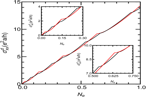
In Fig. 7, we plot as a function of the dimensionless carrier density for (black line) and (red line). The relevant relaxation time is given by Eq. (33) in appendix. The factor can be approximated by the Thomas-Fermi wave vector with the relative dielectric constant and the density of states at the Fermi level. We can see that increases almost linearly from with the peaks at critical value of . These peaks appear when the subbands start to be occupied by electrons,. Also, this behaviour is consistent with the band structures, cf. Fig. 3. These jumps are absent in the conductivity of graphene [16]. Further, we observe the richer structure of peaks for semiconducting ribbons than metallic ones due to the opening of gaps among the subbands of semiconducting nanoribbons as can be seen by comparing the left and right panels of Fig. 3. It is worth mentioning that this scattering-dependent contribution was not accounted for in previous studies, see, e.g., Refs. [2], [5].
III.4 Nondiagonal conductivity in AGNRs
With Eq. (12) becomes
| (23) | |||||
where and are the nondiagonal matrix elements of the velocity operator. Further, the velocity matrix element (6) is diagonal in , therefore will be suppressed in order to simplify the notation. The summation in Eq. (23) runs over all quantum numbers ,, , , and . The parameter , that takes into account the level broadening, is assumed to be independent of the band and subband indices i.e. . Also, we will simplify the notation over summation by considering the subband orthogonality . Hence, after expanding the fraction, Eq. (23) can be rewritten as
| (24) | |||||
We evaluate Eq. (24) by considering the summation over , , and , , denoted by and . For the contributions and to are not allowed due to the condition , cf. Eqs. (6), (11). Hence, the summation over is given only by the Drude-type, intraband contribution to the total conductivity, see Eqs. (15), (17).
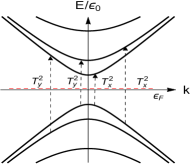
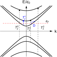
with and the maximum value of below for which the theory is valid. Further, [see Eq. (6)], , and . In the limit , the real and imaginary parts of the nondiagonal conductivity will vanish as is evident from Eqs. (25)-(26). Further, for and , the real part [see Eq. (25)] of the nondiagonal conductivity survives whereas the imaginary one vanishes [see Eq. (26)]. Also, it can be seen from Eqs. (25) and (26) that transitions occur between the valence and conduction band with the same index . Some of these transitions are shown schematically in Fig. 8 for two values of the Fermi level (dashed red lines) with and denoting the intraband and interband ones, respectively at the peaks of and .
For and in the gap we have and . After evaluating the integrals over in Eqs. (25)-(26) we rewrite them in the combined form
| (27) |
where , , , , and .
For we follow the same procedure and from the sum over , cf. Eq. (7), we keep only the dominant terms . We then obtain
| (28) | |||||
and
| (29) | |||||
where , and with . According to Eqs. (28) and (29), the absorption occurs between the valence band with index and the conduction band with . The integrals over in Eqs. (28) and (29) are not tractable and we evaluate them numerically.
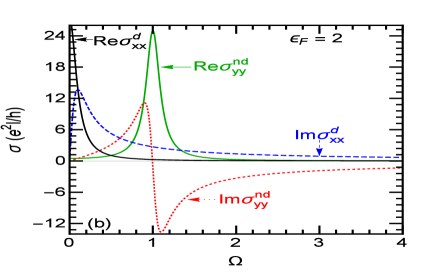
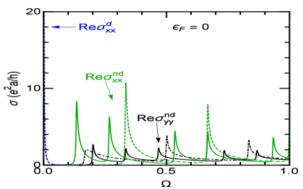
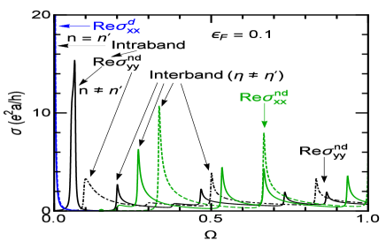
In Fig. 9 we show and as functions of for (upper panel) and (lower panel). The solid curves are for semiconducting nanoribbons and the dotted ones for metallic ribbons . The optical selection rules allow subband index to change by only along the (wire) direction. However, we have along the (confinement) direction, but the amplitude of the peaks is small. Hereafter, we call the transitions satisfying direct transitions and those satisfying indirect transitions. In addition, one needs to go from occupied to unoccupied states through the absorption of photons. The series of peaks corresponding to and occur at and , respectively. These peaks correspond to the allowed interband transitions in the energy spectrum. The position of the absorption peaks follows the same order as indicated in Fig. 8. These results for AGNRs are similar to those in Ref. [5] apart from the contribution which is completely absent and only the real parts of the conductivities are plotted.
In the upper panel of Fig. 9 in which Fermi level is in gap i.e., , we can see that a Drude-type intraband transition is allowed in for due to the nonvanshing velocity matrix elements with [see Eq. (6) and transition in Fig. 8]. On the other hand, we cannot see any type of intraband transitions in because the velocity matrix elements vansh as can be seen from Eq. (6). However, for , only interband absorption transitions are allowed due to the Pauli exclusion principle in both and . But, when we move the Fermi level to [see the red dashed curve in Fig. 8], the absorption peak, say , in is suppressed due to the Pauli exclusion principle for in the range whereas a absorption peak due to intraband transition appears in as can be seen in the lower panel of Fig. 9. Moreover, a Drude absorption peaks appear at low in for both and . One note worthy feature is that resonance energies of indirect transitions are appeared between the that are the energies corresponding to absorption peaks of direct transitions.
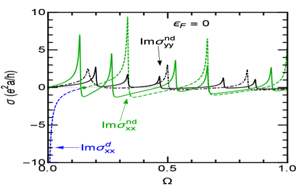
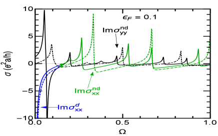
We have plotted and versus the dimensionless photon energy in Fig. 10. The absorption peaks in have negative and positive values due to the negative sign between and terms in Eq. (26), and the peaks corresponding to the transitions and have slightly different energies. This mismatch creates positive and negative peaks in the conductivity. However, the amplitude of the negative peaks is small as compared to that of the positive ones. This argument applies also to [see Eq. (29)].
IV Summary and conclusion
We studied dc and ac transport in both metallic and semiconducting AGNRs. We derived analytical expressions for the diagonal and nondiagonal conductivities by employing linear response theory. We found that semiconducting to metallic transitions occur by changing the number of rows [see Fig. 3] in contrast to ordinary waveguides in which such transitions do not occur, see Fig. 4. In addition, the diagonal conductivity for scattering by screened Coulomb impurities was shown to depend approximately linearly on the carrier density and exhibits upward cusps when the Fermi level crosses the subbands. Further, we showed that the diagonal conductivity varies approximately linearly with the electron concentration in AGNRs, cf. Fig. 7.
Importantly, in all cases we showed that the scattering-dependent conductivity is described quantitatively by a Drude-type contribution which, to our knowledge, was not previously reported or explicitly evaluated. We did show that this contribution dominates the response at very low frequencies at which the usual, scattering-independent contribution near vanishes.
Moreover, we obtained the optical selection rules along the wire and along the confinement direction of AGNRs. We have demonstrated that the peak amplitude of the indirect transitions is suppressed contrary to that of the direct ones. Also, we showed that the absoption of low-energy photons is sensitive to the variation of the Fermi level, in contrast to monolayer WSe2 [17], in which the spectral weight of the interband peaks is continuously redistributed into the intraband ones [see Fig. 9] similar to that of other 2D materials [18] like graphene, silicene, , and topological insulators. A similar behaviour was found for the imaginary part of the conductivity. Furthermore, only intraband transitions occur in ordinary waveguides, cf. Fig. 6 (b) and Eq. (15), in contrast to AGNRs in which both intra- and inter-band transitions occur [see Figs. (9)-(10) and Eqs. (28)- (29)].
The details of the previous paragraphs could best be tested, we think, by optical experiments in AGNRs and by contrasting their results with those in unconfined graphene or other 2D materials and standard waveguides. The peak positions, that are sensitive to the -dependent energy gap between the subbands, cf. Eq. (3), could be tuned by a careful choice of in experiments performed in the far infrared (IR) range. This could lead to the development of new optical devices, in particular novel IR photodetectors based on photon absorption rather than on thermionic emission or tunnelling in arrays of GRNs proposed in Ref. [20]. Moreover, the scattering-dependent contribution to the power spectrum should be evident at very low frequencies at which the other conductivity contributions , as well as in our case, vanish () or nearly so () and dominates the spectrum, cf. Ref. [14]. We are not aware of any such experiments but hope that they will be carried out and also test the selection rules and mentioned above.
Acknowledgements.
M. Z. and P. V. acknowledge the support of the Concordia University Grant No. VB0038 and Concordia University Graduate Fellowship.Appendix A relaxation time
Within the first Born approximation, the standard formula for relaxation time takes the form
| (30) | |||||
where is the impurity potential, the impurity density, and the angle between the initial and final wave vectors. Equation (30) holds only for the elastic scattering. The results for two types of impurity potentials are as follows.
Long-range impurities: For screened, Coulomb-type impurities we consider the model potential [19]
| (31) |
where , is the screening wave vector, the free space permittivity, the static dielectric constant, and is the constant of order in units of inverse length. In this case, we write with the Fourier transform of . We obtain
| (32) | |||||
with and . The integration over is straightforward. That over is carried out using the properties of the function and only the root of the equation contributes to the integral. For simplicity we also take and use . With evaluated at the Fermi level the final result is
| (33) |
where . The term in Eq. (33) denotes the Fermi wave vector for the th subband. In the limit Eq. (33) becomes
| (34) |
Further, for , Eq. (34) reduces to
| (35) |
Short-range impurities: we have with the constant strength of potential and the position of the impurity. In this case, the matrix element becomes . This leads to
| (36) |
For Eq. (36) reduces to
| (37) |
References
- [1] L. Brey and H. A. Fertig, Phys. Rev. B 75, 125434 (2007); H. Zheng, Z. F. Wang, Tao Luo, Q. W. Shi, and J. Chen, ibid. 75, 044710 (2011);
- [2] K.-I. Sakaki, K. Wakabayashi, and T. Enoki, J. Phys. Soc. Jpn. 80, 044710 (2011); M.-F. Lin and F.-L. Shyu, ibid. 69, 3529 (2000); K. Gundra and A. Shukla, Phys. Rev. B 83, 075413 (2011).
- [3] Ken-ichi Sasaki, K. Kato, Y. Tokura, K. Oguri, and T. Sogawa, Phys. Rev. B 84, 085458 (2011).
- [4] L. Brey and H. A. Fertig, Phys. Rev. B 73, 235411 (2006); K. O. Wedel, N. A. Mortensen, K. S. Thygesen, and M. Wubs, Phys. Rev. Lett. 98, 155412 (2018); M. Bahrami and P. Vasilopoulos, Optics Express 25, 16840 (2017).
- [5] Y. Ominato and M. Koshino, Phys. Rev. B 85, 165454 (2012); Solid State Commun. 175-176, 51 (2013).
- [6] J. Liu, Z. Ma, A. R. Wright, and C. Zhang, J. Appl. Phys. 103, 103711 (2008).
- [7] Li Yang, M. L. Cohen, and S. G. Louie, Nano Lett. 7, 3112 (2007).
- [8] K. Wakabayashi, Y. Takane, M. Yamamoto, and M. Sigrist, New J. Phys. 11, 095016 (2009).
- [9] Thomas Aktor, Antti-Pekka Jauho, and Stephen R. Power, Phys. Rev. B 33, 035446 (2016); J. Guo, D. Gunlycke, and C. T. White, Appl. Phys. Lett. 92, 163109 (2008); P. Hawkins, M. Begliarbekov, M. Zivkovic, S. Strauf, and C. P. Search, J. Phys. Chem. C 116, 18382 (2012).
- [10] J. Lan, J.-S. Wang, C. K. Gan, and S. K. Chin, Phys. Rev. B 79, 115401 (2009); Ming-Xing Zhai and Xue-Feng Wang, Sci. Rep. 6, 36762 (2016).
- [11] Ting-Ting Wu, Xue-Feng Wang, Ming-Xing Zhai, Hua Liu, Liping Zhou, and Yong-Jin Jiang, Appl. Phys. Lett. 100, 052112 (2012).
- [12] O. Grning, S. Wang, X. Yao, C. A. Pignedoli, G. B. Barin, C. Daniels, A. Cupo, V. Meunier, X. Feng, A. Narita, K. Múllen, P. Ruffieux, and R. Fasel, Nature 560, 209 (2018); G. Z. Magda, X. Jin, I. Hagymasi, P. Vancso, Z. Osvath, P. Nemes-Incze, C. Hwang, L. P. Biro, and L. Tapaszto, Nature 514, 608 (2014); M. Y. Han, J. C. Brant, and P. Kim, Phys. Rev. Lett. 104, 056801 (2010).
- [13] M. Charbonneau, K. M. Van Vliet, and P. Vasilopoulos, J. Math. Phys. 23, 318 (1982).
- [14] V. Vargiamidis, P. Vasilopoulos and G-Q. Hai, J. Phys.: Condens. Matter 26, 345303 (2014); V. Vargiamidis, and P. Vasilopoulos, J. Appl. Phys. 116, 063713 (2014).
- [15] S. Zhang, R. Liang, E. Zhang, L. Zhang, and Y. Liu, Phys. Rev. B 73, 155316 (2006).
- [16] T. Stauber, N. M. R. Peres, and F. Guinea, Phys. Rev. B 76, 205423 (2007); K. Nomura and A. H. MacDonald, Phys. Rev. Lett. 98, 076602 (2007).
- [17] M. Tahir and P. Vasilopoulos, Phys. Rev. B 94, 045415 (2016).
- [18] Z. Li and J. P. Carbotte, Phys. Rev. B 88, 045414 (2013); E. Illes and E. J. Nicol, ibid. 94, 125435 (2016).
- [19] P. Vasilopoulos and F.M. Peeters, Phys. Rev. B 40, 10079 (1989).
- [20] V. Ryzhii, M Ryzhii, N. Ryabova, V. Mitin, and T. Otsuji, Jpn. J. Appl. Phys. 48, 04C144 (2009).