Electronic polarizability as the fundamental variable in the dielectric properties of two-dimensional materials
Abstract
The dielectric constant, which defines the polarization of the media, is a key quantity in condensed matter. It determines several electronic and optoelectronic properties important for a plethora of modern technologies from computer memory to field effect transistors and communication circuits. Moreover, the importance of the dielectric constant in describing electromagnetic interactions through screening plays a critical role in understanding fundamental molecular interactions. Here we show that despite its fundamental transcendence, the dielectric constant does not define unequivocally the dielectric properties of two-dimensional (2D) materials due to the locality of their electrostatic screening. Instead, the electronic polarizability correctly captures the dielectric nature of a 2D material which is united to other physical quantities in an atomically thin layer. We reveal a long-sought universal formalism where electronic, geometrical and dielectric properties are intrinsically correlated through the polarizability opening the door to probe quantities yet not directly measurable including the real covalent thickness of a layer. We unify the concept of dielectric properties in any material dimension finding a global dielectric anisotropy index defining their controllability through dimensionality.
keywords:
Dielectric screening, electronic polarizability, two-dimensional material, scaling relation, first principles simulations, dielectric anisotropyT. T. and D. S. contributed equally to this work \altaffiliationT. T. and D. S. contributed equally to this work
1 Introduction
The dielectric constant (also known as the relative permittivity) plays a crucial role in bridging various fundamental material properties, such as bandgap 1, 2, optical absorption3 and conductivity 4 with elemental interactions. The central place of in solid-state physics drives the analysis of several phenomena where is common to classify a material accordingly to its ability to screen an electric field in terms of insulators, metals and semiconductors. Such definitions determine a broad range of condensed matter physics, as well as in related fields in chemistry and materials science. The ability to compute and measure in bulk materials is well established via different theoretical 5, 6 and experimental techniques 7 of distinct flavors where the probe of the dielectric properties is made through an external electric field. Despite its obvious appeal, however, it is still unknown whether such quantity can determine the electronic and dielectric properties of two-dimensional (2D) materials 8. The confined nature of such atomically-thin 2D crystals associated with the attenuated and anisotropic character of the dielectric screening 9, 10, 11, 12, 13, 14, 15 has generated long-standing debates whether the dielectric constant truly represents the dielectric features of such low-dimensional systems. The controversy of values reported by both theoretical and experimental approaches can be widely seen throughout the specialized literature, see Ref.16 for a summary, where the variation of can be more than one order of magnitude. As a consequence, several key physical parameters that scale with , such as the exciton binding energy and Debye screening length, cannot be reliably estimated due to the discrepancy of the reported magnitudes of .
Here, by using a combination of analytical and numerical models liaised with highly-accurate first-principles methods involving high-throughput screening techniques, we show that the dielectric constant does not provide a reliable description of the screening features of a 2D material. The interplay between local electrostatic interactions in the monolayer and the volume dependence in the definition of makes such quantity questionable. We propose however that the electronic polarizability that describes the electron dipole in the 2D material as the true descriptor of its dielectric nature. We overcome several problems intrinsic to thin layers not achievable using conventional effective dielectric medium models, such as the real thickness of a monolayer and any dependence on the long-range Coulomb potential. We unveil universal scaling relations between electronic and dielectric properties through the electronic polarizability, such as band gaps, optical spectra and exciton radius, for the current library of known 2D materials involving different lattice symmetries, atomic elements and chemical and physical properties. Moreover, the concept of electronic polarizabilities bridges the gap between the dielectric properties of 2D and 3D systems through a novel dielectric anisotropy index that generalized the concept of dielectric control using dimensionality and bandgap. Our results open a new avenue for the study of the dielectric properties of 2D compounds using techniques yet to be explored.
2 Results and discussions
2.1 Lattice-dependency of macroscopic dielectric constant
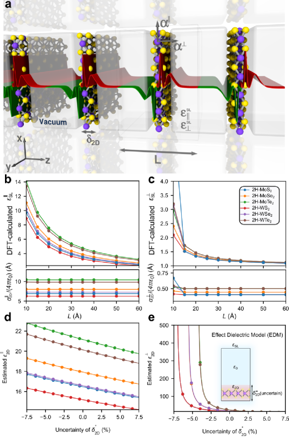
We first approach the discrepancy of macroscopic dielectric constant of 2D materials, by showing that the current definition of used in layered materials is ill-defined. This can be viewed in a model system as illustrated in Figure 1, where an isolated 2D material is placed in the xy-plane of a periodically repeating superlattice (SL) with a length along the z-direction separating the cell images. The static macroscopic dielectric tensor from the superlattice , is determined through fundamental electrostatics by the response of the polarization density under small perturbative external field , where , determine their directions, respectively 4:
| (1a) | |||||
| (1b) | |||||
where is the dielectric tensor of the environment, is the total dipole moment within the SL, is the spatial charge density, is the volume of the supercell, is the xy-plane area of the SL and is vacuum permittivity. Here we limit our study on the electronic contributions to the macroscopic dielectric constant where the dipole results from the response of the electron density under an external field. Ionic contributions17 to have previously been shown to be negligible18 and are not considered here. The symmetry of 2D materials leads to inappreciable off-diagonal elements of the dielectric tensor (), while the diagonal elements , and can be different 19. Considering that the 2D material is placed in vacuum ( and ), we can distinguish two components of , namely the in-plane () and out-of-plane () dielectric constants, where and . The absence of bonding perpendicular to the plane confines the induced dipole moments along the z-direction within a range of 5–6 Å into the vacuum (Figure 1a and Supplementary Figure LABEL:SI-fig:rho-profile). Under a given external field, the strong confinement of the induced dipole moment causes the integral in the numerator of Eq. 1b to be converged within few Å’s resulting that the dipole moment from the periodic supercell images do not mutually interfere.
Conversely, the increase of in the denominator of Eq. 1b dilutes the polarization density, and in turn makes both and dropping to unity when is infinitely large, which is not physical. Despite the simplicity of this argument, any calculation performed using such definition will intrinsically depend on the magnitude of , an artificial parameter introduced by the simulation setup. This dependence can be clearly demonstrated by plotting and calculated from density functional theory (DFT) (see Theoretical Methods for details) as a function of for P6̄m2 transition metal dichalcogenides (TMDCs), 2H-MX2, where M=Mo, W and X=S, Se, Te (top panels of Figure 1b and 1c, respectively). To obtain a better description of the electronic band structure, the calculations of dielectric properties were performed at the level of Heyd-Scuseria-Ernzerhof (HSE06) hybrid functional 20, 21. Both components of the dielectric constant decrease with as excepted. To rule out the possibility that the result is affected by the choice of the functional, we performed simulations at higher levels of theory using many-body techniques (G0W0), which invariably give alike results (see Supplementary Figure LABEL:SI-fig:GW-PBE-alpha). The lattice-size dependency also exists for the dielectric function in the frequency domain.
We carried out similar analysis for frequency-dependent and using different approaches including Perdew-Burke-Ernzerhof (PBE) exchange-correlation functional 22, 23, 24, G0W025 and Bethe-Salpeter equation (G0W0BSE)26 (see Supplementary Section LABEL:SI-ssec:gw and Supplementary Figures LABEL:SI-fig:PBE-omega-inLABEL:SI-fig:BSE-omega-out). Despite the various levels of theory analyzed and the increased accuracy of the calculated optical properties due to the inclusion of many-body screening and excitonic effects, the magnitude of the dielectric function universally decreases with over the frequency. The underlying physical reason for such dependence can be noticed in the definition of the dielectric function versus shown in Eqs. LABEL:SI-eq:dft-dielectricLABEL:SI-eq:dft-dielectric-real, which also depend on the volume of the unit cell. These results indicate that any quantity that depends on and , such as the optical absorption (), refractive index () and electron energy loss spectrum (EELS, ), suffers the same deficiencies for 2D materials.
2.2 The electronic polarizability of 2D materials
To solve the problem described above, we need to find the -independent alternative of , which is related to both electrostatic and optical properties of a 2D material 27. By multiplying Eq. 1b with , we obtain the sheet polarization density, that is, , along the direction . Following the discussion in the previous section, becomes independent of the lattice size when is large enough, due to the short decay of the induced charge density into the vacuum (see Supplementary Figure LABEL:SI-fig:rho-profile). Similar to the molecular polarizability28, we utilize the concept of electronic polarizability , which has been used previously to solve exciton-related problems in 2D materials 12, 29, 30. is a macroscopic quantity that characterizes the ability to induce dipole moments in a 2D material, and is associated with through: 31, where is the cell-averaged “local” electric field acting on the 2D material to induce polarization. Alike to , is also a macroscopic quantity that excludes the fields generated by the dipoles of the 2D sheet from . Note the term “local” in is adapted to resemble the Lorentz model32 which has also been used for other low-dimensional materials (e.g. nanotube33 and molecules31, and should be distinguished with the microscopic local field which is spatially changing.
Such macroscopic treatment of polarizability is valid when the length of the superlattice is significantly larger than the spatial distribution of induced charges. At limit, can be solved using electrostatic boundary conditions of the slab geometry 34, 35. The continuity of the electric field along the in-plane direction gives , while for the out-of-plane component, the dipole screening yields 35, 31, where and are the external field along the in-plane and out-of-plane directions, respectively. Combining with Eqs. 1a and 1b, and can be related with and , respectively:
| (2a) | |||||
| (2b) | |||||
Using these relations, we show that the calculated and of the selected TMDCs as a function of in the bottom panels of Figure 1b and 1c, respectively. In contrast to and , we observe that both and reach convergence when 10 Å15 Å, respectively. Such results are in good agreement with the spatially localized induced dipole moment of a 2D material as shown in Supplementary Figure LABEL:SI-fig:rho-profile. Equations 2a2b can also be used to remove the dependence on for and , generating lattice-independent electronic polarizability and in the frequency domain, respectively (see details in Supplementary Section LABEL:SI-ssec:gw). These findings indicate that the electronic polarizability captures the essence of the dielectric properties of 2D materials. In contrast to the ill-defined macroscopic , has a unique definition, and does not suffer from the dependency on the lattice size. It is worthy mentioning that Eqs.2a2b were obtained using purely electrostatic arguments without any assumption regarding the medium where the 2D material is immersed or a capacitance model where an effective dielectric response can be extracted. More details about the choice of the 2D polarizability, comparison with other methods, simulations at the frequency-dependent domain can be found in Supplementary Section LABEL:SI-ssec:gw.
2.3 Comparison with the effective dielectric model (EDM)
Apart from the 2D electronic polarizability proposed here, the effective dielectric model (EDM) is commonly used in literature to treat the 2D material as a slab with an effective dielectric tensor and thickness . Such method can be found in both experimental and theoretical studies, such as to interpret ellipsometry data 36, 37, 38, 39, reflectance / transmission spectra 40, 41, optical conductance 27 and many-body interactions 19, 42 of 2D materials. The EDM allows applying physical concepts of bulk systems directly to their 2D counterparts using . However, there are several drawbacks of such approach. For instance, the wavevector -dependency of dielectric screening in 2D sheets 12, 29, 43 is not captured. More severely, here we show that, due to the uncertainty of , the calculated , in particular its out-of-plane component, is extremely sensitive to the choice of , making such model questionable.
The basic assumption of EDM can be seen in the inset of Figure 1e, where the macroscopic is considered to be composed by (i) a 2D slab with an effective dielectric constant and a thickness , and (ii) a vacuum spacing with distance . Using the effective medium theory (EMT) 44, 34, the relation between and can be expressed using capacitance-like equations 27, 45, 46:
| (3a) | |||||
| (3b) | |||||
In principle, both the values of and are unknown for a certain 2D material. To minimize the modeling error, we used non-linear least-square fitting to extract and of selected 2H TMDCs simultaneously from ab initio – data in Figure 1b and 1c (see details in Supplementary Figure LABEL:SI-fig:rescale-prb). The fitted values of the slab thickness, and from in-plane and out-of-plane data, respectively, are shown in Supplementary Table LABEL:SI-tab:delta-L-DFt. Although the uncertainty only corresponds to a few percent of the interlayer spacing in the bulk structure of these 2D materials, its influence on the calculated values and is substantial. We estimated the dispersion of and considering slightly deviations of from the best fitted value by 7.5% (Figures 1d and 1e). Strikingly, decays linearly with , while spans over more than one order of magnitude. The sensitivity of to explains the discrepancy in literature for both isotropic 19 and highly anisotropic 27, 45 tensors on 2D materials extracted using EDM. As a consequence, the estimated values of , in particular its out-of-plane component, are highly controversial.
On the contrary, the proposed approach does not suffer from such limitations, despite its relatively simple formalism. The relative uncertainty of is generally at the order of 10-4 (Supplementary Figure LABEL:SI-fig:alpha-converg). In addition, the calculation of is technically simpler than : (i) can be achieved using single-point calculation of macroscopic dielectric tensor, while requires non-linear fitting of multiple – data points; (ii) the values of typically converge well for (20 Å), while suffers from the uncertainties as described above.
2.4 Universal scaling laws of
For bulk materials, pioneering works from the 1950s had demonstrated empirical equations between and the bandgap , including the Moss 1, 2, 47 or Ravindra 48, 49 relations. Such universal relations, if exist in the context of , would be of high importance for studying and predicting the screening of 2D materials. Inspired by the random phase approximation (RPA) theory 5 within the formalism3, 30, we propose the following universal relations for and , for 2D materials (see Supplementary Section LABEL:SI-sec:theory-1 for details):
| (4a) | |||||
| (4b) | |||||
where is the fundamental electronic bandgap and is the intrinsic thickness of the 2D layer, with coefficients 30, where is a pre-factor associated with the band degeneracy, and . It is worth noting, unlike the parameter that is artificially assigned within the EDM picture (see previous section), can be uniquely defined by , a quantity that can be
computationally and experimentally determined. Despite the simplicity of Eqs. 4a and 4b, they generate direct relationships between the electronic polarizability and the electronic/structural properties for any 2D material in a new framework.
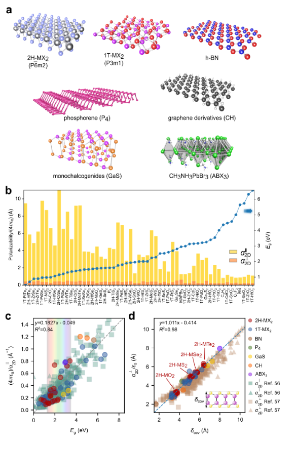
Next, we show that these equations are valid for the current library of known layered materials involving different lattice symmetry, element composition, optical and electronic properties (Figure 2a). A high-throughput screening performed on different families of TMDCs (MX, where M is a metal in groups 4, 6, 10, and X=O, S, Se, Te) and phases (P6̄m2, P3m1), metal monochalcogenides (Ga2S2, Ga2Se2), cadmium halides (CdX2, X=Cl, I), hexagonal boron nitride (BN), graphene derivatives (fluorographene (C2F2), graphane (C2H2)), phosphorene (P4) and thin layer organic-inorganic perovskites (ABX3), shows that our method enables full correlation between these disparate variables. Figure 2b compares the calculated fundamental bandgap (blue dots) and 2D electronic polarizabilities (bar plots) of all the 2D materials investigated, covering a wide spectrum range from far-infrared to ultraviolet. Note that from dimension analysis, it is more intuitive to express the polarizability as , which has unit of Å. We find that has a general descending trend when increases, while no apparent correlation between and is observed (see Supplementary Section LABEL:SI-sec:pol-2D-Eg). We then examine Eqs. 4a and 4b using the polarizabilities by first-principle calculations. Figure 2c shows (in Å-1) as a function of (in eV) for the 2D materials investigated using HSE06 hybrid functional (circular dots) and PBE (triangles and squares). A linear regression coefficient of indicates a strong correlation between bandgaps and polarizabilities as predicted in Eq. 4a. We also discovered that the linearity between and (measured by the value) is higher when the bandgap is calculated using the HSE06 hybrid functional compared with that from PBE exchange-correlation functional (see Supplementary Section LABEL:SI-sec:pol-2D-Eg and Supplementary Figure LABEL:SI-fig:alpha-Eg-diff). This is reasonable as the bandgaps for 2D materials obtained at the PBE functional, although may be close to experimental reported optical transition energies, are an artifact of the simulation due to a fortuitous error cancellation52, 53. Thus, the use of a time-consuming hybrid functional in our study is justified. A detailed benchmark of Eqs. 4a and 4b using different bandgaps, databases, and levels of theory can be seen in Supplementary Sections LABEL:SI-sec:pol-2D-EgLABEL:SI-sec:gpaw.
We further examine the validity of Eq. 4b, that is, the relation between and the thickness of a 2D material. To test if the quantity is physical, we choose the “covalent” thickness as a comparison. is defined as the longest distance along the z-direction between any two atom nuclei plus their covalent radii:
| (5) |
where , are atomic indices in the 2D material and is the covalent radius of atom (inset in Figure 2d). As shown in Figure 2d, (or equivalently, ) is very close to with a good linear correlation of . This result indicates a strong relation between and the geometry of the 2D layer, which can be approximated by . Similar to the molecular polarizability which characterizes the volume of the electron distribution of an isolated molecule 28, is also naturally related to the characteristic thickness of the electron density of a 2D material. Supplementary Section LABEL:SI-ssec:theory-1-perp-fundamental shows an explanation of this behavior from fundamental electrostatics and why is close to . The geometric nature of leads to several interesting properties. For instance, the points corresponding to 2H-TMDCs with same chalcogenide element (i.e. 2H-MO2, 2H-MS2, 2H-MSe22 or 2H-MTe2, where M= Mo, W) lie very close in Figure 2b (detailed values see Supplementary Table S2). This can be briefly explained by the fact that the difference between covalent radii of transition metals (e.g. 8 pm between Mo and W) is much smaller than that between group 16 elements (e.g. 40 pm between O and S). Our proposed definition of which is based on Eq. 4b will provide insights on some long-existing controversies about the experimental thickness of 2D materials 54 through a measurable quantity, e.g. 55, 56, 57.
To rule out the possibility that our conclusion are limited by the number of materials used at HSE06 level, we further validate Eqs. 4a and 4b using two different 2D-material databases based on different codes50, 51. We extracted the dielectric properties of over 300 compounds calculated at the PBE level, and superimpose with our results in Figure 2c and 2d. The high-throughput datasets also show linear trends for both (in Å) vs (in eV) (, ) and vs (both in Å, , ) relations. We notice that the linear coefficients are similar but not identical to those calculated at the HSE06 level. The discrepancies may be due to several factors resulted from different choice of functionals, such as the underestimation of the bandgap in PBE, and different description of the exchange-correlation potentials. We note that a more accurate estimation of the coefficients should be performed with larger datasets and accurate functionals which requires further work. Nevertheless, the validity of the linear trends observed for and is undeniable. We have also searched for additional relations between the 2D polarizabilities with other physical quantities, including the effective carrier mass, quantum capacitance (density of states) and total atomic polarizabilities with no apparent correlations being found (Supplementary Section LABEL:SI-sec:gpaw-3).
2.5 Application in multilayer and bulk systems
The concept of electronic polarizability is not limited to monolayer materials, and can be applied to multilayer and bulk systems as well. For a 2D-material stack composed of layers, we can define the electronic polarizability similarly to Eqs. 2a2b by replacing to . To check whether such assumption is valid, Figure 3a and 3b show and as functions of for several TMDCs in 2H-phase, respectively. Interestingly, we find that in all cases, exhibits nearly ideal linear relation with , such that and . Due to the relatively small applied electric field (0.01 eV/Å), the interlayer interactions within the stack are negligible. Under such circumstances, of individual layers is additive, which leads to the following general relation:
| (6) |
where is the electronic polarizability of layer , and is the direction of the polarization. This relation can be additionally utilized to calculate screening inside 2D heterostructures 58, 59.
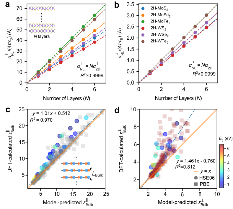
In a bulk material with an equilibrium inter-layer distance , we can follow a similar procedure as in multilayer by defining the polarizability as . Inspired by Eqs. 2a and 2b, the dielectric constants and of the bulk layered material can be reconstructed by and as:
| (7a) | ||||
| (7b) | ||||
Here we neglect the effect of the stacking order of the layers and hypothesized that the basic building blocks for the dielectric response of the bulk are the polarizability of the individual layers subject to vdW and electrostatic interactions. The dielectric constant although not well-defined for a monolayer 2D material becomes applicable when the 2D layers are put together as shown in the following. We compare the values of and computed from DFT simulations (y-axis) with those predicted using Eqs 7a and 7b (x-axis) as shown in Figure 3c and 3d. Strikingly both HSE06 and PBE datasets give almost identical results which suggest a non-method dependent behavior. We observe that values calculated by DFT and predicted by Eq. 7a are in sound agreement with a linear regression slope of 1.01 and of 0.97. Conversely, values predicted from Eq. 7b fairly agree with the DFT-calculated values when eV, while the deviation becomes larger when reduces. The above results indicate that can generally be estimated with high accuracy from its 2D counterpart, while differs due to the interlayer coupling and overlap between induced dipole59, 45. Nevertheless, as most of the optical response and electronic device properties rely on the in-plane dielectric constant for practical applications, the possibility to handily estimate from well established magnitudes of , for instance, from material databases, using reverse engineering in Eq.7a, it is a step forward in the design and understanding of the dielectric phenomena in 2D.
2.6 Unified geometric representation of
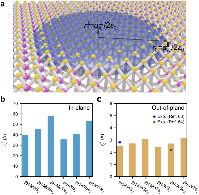
Lastly, we demonstrate that both and can be unified using a geometric approach. In merit of the unit analysis, and both have unit of [Length]. In other words, they represent in- and out-of-plane characteristic lengths, respectively. It is well-known that the in-plane screened electrostatic potential from a point charge as a function of distance 9, 60 (where is the Struve function and is the Bessel function of second kind) is associated with the in-plane screening radius , such that reduces to the simple Coulomb potential in vacuum. Combining with the result that characterizes the thickness of a 2D material, we can view the dielectric screening of a point charge sitting in the middle of a 2D material as an ellipsoid with the radii of principal axes to be and , respectively, as illustrated in Figure 4a. This is analog to the polarizability ellipsoid picture of molecules used in spectroscopy 61. The polarizability ellipsoid for a 2D material is in general ultra flat, with , as demonstrated by layered materials of group 6 of 2H-TMDCs (Figure 4b and 4c). The picture of the polarizability ellipsoid provides further insights into the physical nature of : is close to the exciton radius that it is confined within the 2D plane 60. This radius is generally larger for a smaller bandgap semiconductor, and can be converted through the exciton binding energy as proposed in Refs.29, 30. in its turn can be indirectly deduced from Stark effect for perpendicular electric fields 62, 63, 64. A comparison with available experimental data65, 64 gives close magnitudes with our predicted values.
Inspired by the polarizability ellipsoid model, we will show that a general picture of the dielectric properties in any dimension can be drawn by studying the dielectric anisotropy. That is, the dielectric response of a material along its different geometrical orientations. We define the dielectric anisotropy index as:
| (8) |
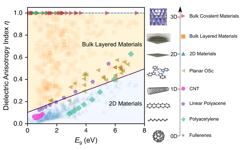
indicates that the material has isotropic dielectric properties while means that the dielectric property is highly anisotropic. Figure 5 shows the phase diagram of as function of for 2D materials and their bulk counterparts. Interestingly, the 2D materials (blue triangles) can be clearly distinguished from the bulk layered materials (orange squares) with the boundary line determined to be . The much lower values for 2D materials compared with their bulk counterparts indicates a high dielectric anisotropy, which is responsible for the unique 2D optoelectronic properties, such as the electrostatic transparency phenomena66, 67, 68 and the large exciton binding energies 60, 69, 70, 71. From Eqs. 4a, 4b and 8 we can see is roughly proportional to , which explains the observation that for 2D materials increase almost linearly with , since the layer thickness (mostly 3–10 Å) of the 2D materials investigated varies much less than in the range of 0.1–7 eV (Figure 2b2c). Further analysis shows that the dielectric anisotropy index of any bulk layered material obeys , where is the anisotropy index of corresponding 2D layer, which is the basis for the separation of bulk and 2D regimes in the phase diagram (Supplementary Section LABEL:SI-sec:aniso). For comparison, we also superimpose the dielectric anisotropy indices of common semiconducting materials in other dimensions on the phase diagram in Figure 5. Bulk covalent 3D (e.g. Si, GaN) and 0D (e.g. fullerenes) semiconductors show isotropic dielectric properties, scattered along the line . Conversely, reduced dimensionality increases the dielectric anisotropy of materials such as planar organic semiconductor (OSc) in 1D-2D (e.g. CuPc), carbon nanotube (CNT) in 1D, linear OSc in 0D-1D (e.g. polyacene and polyacetylene). Interestingly, most of these materials also scatter along the boundary line separating the bulk and 2D regimes, indicating that the criteria distinguishing 2D (more anisotropic) and bulk materials (more isotropic) from the diagram, can also be applied to other dimensions. From the phase diagram, we can see that 2D and bulk layered materials, including 2D van der Waals heterostructure (vdWH)8, provides more flexibility in controlling the dielectric and electronic properties, compared with covalent semiconductors (without vdW gaps) in other dimensions.
3 Conclusion
Our results show that the 2D electronic polarizability is a local variable determining the dielectric properties of 2D materials. There exist well-defined relationships between and other quantities hidden in the electronic properties. According to our analysis, simple scaling equations involving bandgap and layer thickness can be used to describe both dielectric and electronic features at the same footing. A dielectric anisotropy index is found relating any material dimension with its controllability. Thus, our results suggest that the challenge of understanding the dielectric phenomena is in general a geometrical problem mediated by the bandgap. We believe the principles presented here will benefit both fundamental understanding of 2D materials as well as a rational device design and optimization.
4 Theoretical Methods
Simulations were carried out using plane-wave density functional theory package VASP 72, 73, 74 using the projector augmented wave (PAW) approach with GW pseudopotentials 75. Band gaps were calculated using the Heyd-Scuseria-Ernzerhof hybrid functional (HSE06) 20, 21, with spin orbit coupling (SOC) explicitly included. The geometries were converged both in cell parameters and ionic positions, with forces below 0.04 eV/Å. To ensure the accuracy of dielectric property of monolayer, a vacuum spacing of 15 Å is used. A k-point grid of was used to relax the superlattice, with an initial relaxation carried out at the Perdew-Burke-Ernzerhof (PBE)22, 23, 24 exchange-correlation functional level and a subsequent relaxation carried out at HSE06 level, allowing both cell parameters and ionic positions to relax each time. In VASP, the tag PREC=High was used, giving a plane wave kinetic energy cutoff of 30% greater than the highest given in the pseudopotentials used in each material. This guarantees that absolute energies were converged to a few meV and the stress tensor to within 0.01 kBar. Calculation of the macroscopic ion-clamped dielectric tensor were carried out with an 18181 k-grid and electric field strength of 0.001 eV/Å. Local field effect corrections are included at the exchange-correlation potential at both PBE and HSE06 levels. The materials from Ref.50 for comparison were choses with the GW bandgap larger than 0.05 eV. Bulk layered materials were constructed by relaxing the c-axis length of corresponding monolayer material with the interlayer van der Waals (vdW) interactions calculated by non-local vdW correlation functional76. The dielectric properties of bulk layered materials using VASP were calculated at HSE06 level with 18186 k-grid with same parameter as for monolayer, while the dielectric properties of bulk counterparts of Ref. 50 are calculated at PBE level with a k-point density of 10 Å-1. Local field effect corrections are also used for the dielectric properties of bulk systems.
Data Availability
The data that support the findings of this study is available within the paper and its Supplementary Information.
Competing interests
The Authors declare no conflict of interests.
Acknowledgments
C.J.S. and T.T. are grateful for financial support from ETH startup funding. L.H.L. thanks the financial support from Australian Research Council (ARC) via Discovery Early Career Researcher Award (DE160100796). E.J.G.S. acknowledges the use of computational resources from the UK Materials and Molecular Modelling Hub for access to THOMAS supercluster, which is partially funded by EPSRC (EP/P020194/1); and CIRRUS Tier-2 HPC Service (ec019 Cirrus Project) at EPCC (http://www.cirrus.ac.uk) funded by the University of Edinburgh and EPSRC (EP/P020267/1). The Department for the Economy (USI 097) is acknowledged for funding support.
Author Contributions
E.J.G.S. conceived the idea and supervised the project. T.T., D.S., D.H. and E.J.G.S. performed the first-principles simulations and data analytics. T.T. developed the analytical model with inputs from E.J.G.S. and C.J.S. L.H.L. and J.N.C. performed numerical analysis and contributed to the discussions together with M.C. E.J.G.S. and T.T. co-wrote the manuscript with inputs from all authors. All authors contributed to this work, read the manuscript, discussed the results, and all agree to the contents of the manuscript.
Supporting Information
The Supporting Information contains detailed descriptions and discussions about dielectric properties of 2D materials, effective dielectric model, derivations of the 2D polarizability-based model, dependency of on the choice of bandgap, relation between 2D and 3D properties, explanations of the dielectric anisotropy, as well as raw data sheet from first principles calculations.
References
- Moss 1950 Moss, T. S. A Relationship between the Refractive Index and the Infra-Red Threshold of Sensitivity for Photoconductors. Proc. Phys. Soc. B 1950, 63, 167
- Moss 1985 Moss, T. S. Relations between the Refractive Index and Energy Gap of Semiconductors. Phys. Status Solidi B 1985, 131, 415–427
- Kittel 2005 Kittel, C. Introduction to solid state physics; Wiley, 2005
- Dressel and Gruner 2001 Dressel, M.; Gruner, G. Electrodynamics of solids: optical properties of electrons in matter; Cambridge University Press, 2001
- Adler 1962 Adler, S. L. Quantum Theory of the Dielectric Constant in Real Solids. Phys. Rev. 1962, 126, 413–420
- Hybertsen and Louie 1987 Hybertsen, M. S.; Louie, S. G. Ab initiostatic dielectric matrices from the density-functional approach. I. Formulation and application to semiconductors and insulators. Phys. Rev. B 1987, 35, 5585–5601
- Palik 1998 Palik, E. D., Ed. Handbook of optical constants of solids; Academic Press, 1998
- Novoselov et al. 2016 Novoselov, K. S.; Mishchenko, A.; Carvalho, A.; Castro Neto, A. H. 2D materials and van der Waals heterostructures. Science 2016, 353, aac9439
- Keldysh 1979 Keldysh, L. V. Coulomb interaction in thin semiconductor and semimetal films. Sov. Phys. JETP 1979, 29, 658
- Sharma 1985 Sharma, A. Dielectric function of a semiconductor slab. J. Phys. C: Solid State Phys. 1985, 18, L153–L156
- Low et al. 2014 Low, T.; Roldán, R.; Wang, H.; Xia, F.; Avouris, P.; Moreno, L. M.; Guinea, F. Plasmons and Screening in Monolayer and Multilayer Black Phosphorus. Phys. Rev. Lett. 2014, 113, 106802
- Cudazzo et al. 2011 Cudazzo, P.; Tokatly, I. V.; Rubio, A. Dielectric screening in two-dimensional insulators: Implications for excitonic and impurity states in graphane. Phys. Rev. B 2011, 84, 085406
- Bechstedt et al. 2012 Bechstedt, F.; Matthes, L.; Gori, P.; Pulci, O. Infrared absorbance of silicene and germanene. Appl. Phys. Lett. 2012, 100, 261906
- Cudazzo et al. 2010 Cudazzo, P.; Attaccalite, C.; Tokatly, I. V.; Rubio, A. Strong Charge-Transfer Excitonic Effects and the Bose-Einstein Exciton Condensate in Graphane. Phys. Rev. Lett. 2010, 104, 226804
- Nazarov 2015 Nazarov, V. U. Electronic excitations in quasi-2D crystals: what theoretical quantities are relevant to experiment? New J. Phys. 2015, 17, 073018
- Li et al. 2016 Li, S.-L.; Tsukagoshi, K.; Orgiu, E.; Samorì, P. Charge transport and mobility engineering in two-dimensional transition metal chalcogenide semiconductors. Chem. Soc. Rev. 2016, 45, 118–151
- Sohier et al. 2017 Sohier, T.; Gibertini, M.; Calandra, M.; Mauri, F.; Marzari, N. Breakdown of Optical Phonons’ Splitting in Two-Dimensional Materials. Nano Lett. 2017, 17, 3758–3763
- Laturia and Vandenberghe 2017 Laturia, A.; Vandenberghe, W. G. Dielectric properties of mono- and bilayers determined from first principles. 2017 International Conference on Simulation of Semiconductor Processes and Devices (SISPAD). 2017; pp 337–340
- Sohier et al. 2016 Sohier, T.; Calandra, M.; Mauri, F. Two-dimensional Fröhlich interaction in transition-metal dichalcogenide monolayers: Theoretical modeling and first-principles calculations. Phys. Rev. B 2016, 94, 085415
- Heyd et al. 2003 Heyd, J.; Scuseria, G. E.; Ernzerhof, M. Hybrid functionals based on a screened Coulomb potential. J. Chem. Phys. 2003, 118, 8207–8215
- Heyd et al. 2006 Heyd, J.; Scuseria, G. E.; Ernzerhof, M. Erratum: “Hybrid functionals based on a screened Coulomb potential” [J. Chem. Phys. 118, 8207 (2003)]. J. Chem. Phys. 2006, 124, 219906
- Perdew et al. 1996 Perdew, J. P.; Burke, K.; Ernzerhof, M. Generalized Gradient Approximation Made Simple. Phys. Rev. Lett. 1996, 77, 3865–3868
- Ernzerhof and Scuseria 1999 Ernzerhof, M.; Scuseria, G. E. Assessment of the Perdew–Burke–Ernzerhof exchange-correlation functional. J. Chem. Phys. 1999, 110, 5029–5036
- Paier et al. 2005 Paier, J.; Hirschl, R.; Marsman, M.; Kresse, G. The Perdew–Burke–Ernzerhof exchange-correlation functional applied to the G2-1 test set using a plane-wave basis set. J. Chem. Phys. 2005, 122, 234102
- Hedin 1965 Hedin, L. New Method for Calculating the One-Particle Green’s Function with Application to the Electron-Gas Problem. Phys. Rev. 1965, 139, A796–A823
- Onida et al. 2002 Onida, G.; Reining, L.; Rubio, A. Electronic excitations: density-functional versus many-body Green’s-function approaches. Rev. Mod. Phys. 2002, 74, 601–659
- Matthes et al. 2016 Matthes, L.; Pulci, O.; Bechstedt, F. Influence of out-of-plane response on optical properties of two-dimensional materials: First principles approach. Phys. Rev. B 2016, 94, 205408
- Israelachvili 2011 Israelachvili, J. N. Interactions Involving the Polarization of Molecules. Intermolecular and Surface Forces 2011, 91–106
- Olsen et al. 2016 Olsen, T.; Latini, S.; Rasmussen, F.; Thygesen, K. S. Simple Screened Hydrogen Model of Excitons in Two-Dimensional Materials. Phys. Rev. Lett. 2016, 116, 056401
- Jiang et al. 2017 Jiang, Z.; Liu, Z.; Li, Y.; Duan, W. Scaling Universality between Band Gap and Exciton Binding Energy of Two-Dimensional Semiconductors. Phys. Rev. Lett. 2017, 118
- Tobik and Dal Corso 2004 Tobik, J.; Dal Corso, A. Electric fields with ultrasoft pseudo-potentials: Applications to benzene and anthracene. J. Chem. Phys. 2004, 120, 9934–9941
- Wiser 1963 Wiser, N. Dielectric Constant with Local Field Effects Included. Phys. Rev. 1963, 129, 62––69
- Benedict et al. 1995 Benedict, L. X.; Louie, S. G.; Cohen, M. L. Static polarizabilities of single-wall carbon nanotubes. Phys. Rev. B 1995, 52, 8541–8549
- Markel 2016 Markel, V. A. Introduction to the Maxwell Garnett approximation: tutorial. J. Opt. Soc. Am. A 2016, 33, 1244
- Meyer and Vanderbilt 2001 Meyer, B.; Vanderbilt, D. Ab initiostudy of BaTiO3 and PbTiO3 surfaces in external electric fields. Phys. Rev. B 2001, 63, 205426
- Wurstbauer et al. 2010 Wurstbauer, U.; Röling, C.; Wurstbauer, U.; Wegscheider, W.; Vaupel, M.; Thiesen, P. H.; Weiss, D. Imaging ellipsometry of graphene. Appl. Phys. Lett. 2010, 97, 231901
- Yim et al. 2014 Yim, C.; O’Brien, M.; McEvoy, N.; Winters, S.; Mirza, I.; Lunney, J. G.; Duesberg, G. S. Investigation of the optical properties of MoS2 thin films using spectroscopic ellipsometry. Appl. Phys. Lett. 2014, 104, 103114
- Shen et al. 2013 Shen, C.-C.; Hsu, Y.-T.; Li, L.-J.; Liu, H.-L. Charge Dynamics and Electronic Structures of Monolayer MoS 2 Films Grown by Chemical Vapor Deposition. Appl. Phys. Express 2013, 6, 125801
- Li et al. 2014 Li, W.; Birdwell, A. G.; Amani, M.; Burke, R. A.; Ling, X.; Lee, Y.-H.; Liang, X.; Peng, L.; Richter, C. A.; Kong, J.; Gundlach, D. J.; Nguyen, N. V. Broadband optical properties of large-area monolayer CVD molybdenum disulfide. Phys. Rev. B 2014, 90, 195434
- Li et al. 2014 Li, Y.; Chernikov, A.; Zhang, X.; Rigosi, A.; Hill, H. M.; van der Zande, A. M.; Chenet, D. A.; Shih, E.-M.; Hone, J.; Heinz, T. F. Measurement of the optical dielectric function of monolayer transition-metal dichalcogenides:MoS2,MoSe2,WS2, andWSe2. Phys. Rev. B 2014, 90, 205422
- Wilson and Yoffe 1969 Wilson, J.; Yoffe, A. The transition metal dichalcogenides discussion and interpretation of the observed optical, electrical and structural properties. Adv. Phys. 1969, 18, 193–335
- Meckbach et al. 2018 Meckbach, L.; Stroucken, T.; Koch, S. W. Influence of the effective layer thickness on the ground-state and excitonic properties of transition-metal dichalcogenide systems. Phys. Rev. B 2018, 97, 035425
- Trolle et al. 2017 Trolle, M. L.; Pedersen, T. G.; Véniard, V. Model dielectric function for 2D semiconductors including substrate screening. Sci. Rep. 2017, 7, 39844
- Aspnes 1982 Aspnes, D. Optical properties of thin films. Thin Solid Films 1982, 89, 249–262
- Laturia et al. 2018 Laturia, A.; Van de Put, M. L.; Vandenberghe, W. G. Dielectric properties of hexagonal boron nitride and transition metal dichalcogenides: from monolayer to bulk. npj 2D Mater. Appl. 2018, 2, 6
- Tancogne-Dejean et al. 2015 Tancogne-Dejean, N.; Giorgetti, C.; Véniard, V. Optical properties of surfaces with supercellab initiocalculations: Local-field effects. Phys. Rev. B 2015, 92, 245308
- Finkenrath 1988 Finkenrath, H. The moss rule and the influence of doping on the optical dielectric constant of semiconductors—II. Infrared Physics 1988, 28, 363–366
- Ravindra and Srivastava 1980 Ravindra, N. M.; Srivastava, V. K. Electronic polarizability as a function of the penn gap in semiconductors. Infrared Phys. 1980, 20, 67–69
- Ravindra and Srivastava 1979 Ravindra, N.; Srivastava, V. Variation of refractive index with energy gap in semiconductors. Infrared Phys. 1979, 19, 603–604
- Haastrup et al. 2018 Haastrup, S.; Strange, M.; Pandey, M.; Deilmann, T.; Schmidt, P. S.; Hinsche, N. F.; Gjerding, M. N.; Torelli, D.; Larsen, P. M.; Riis-Jensen, A. C.; et al., The Computational 2D Materials Database: high-throughput modeling and discovery of atomically thin crystals. 2D Mater. 2018, 5, 042002
- Mounet et al. 2018 Mounet, N.; Gibertini, M.; Schwaller, P.; Campi, D.; Merkys, A.; Marrazzo, A.; Sohier, T.; Castelli, I. E.; Cepellotti, A.; Pizzi, G.; et al., Two-dimensional materials from high-throughput computational exfoliation of experimentally known compounds. Nat. Nanotechnol. 2018, 13, 246–252
- Kuc and Heine 2015 Kuc, A.; Heine, T. The electronic structure calculations of two-dimensional transition-metal dichalcogenides in the presence of external electric and magnetic fields. Chem. Soc. Rev. 2015, 44, 2603–2614
- Lee et al. 2017 Lee, J.; Huang, J.; Sumpter, B. G.; Yoon, M. Strain-engineered optoelectronic properties of 2D transition metal dichalcogenide lateral heterostructures. 2D Materials 2017, 4, 021016
- Shearer et al. 2016 Shearer, C. J.; Slattery, A. D.; Stapleton, A. J.; Shapter, J. G.; Gibson, C. T. Accurate thickness measurement of graphene. Nanotechnology 2016, 27, 125704
- Antoine et al. 1999 Antoine, R.; Dugourd, P.; Rayane, D.; Benichou, E.; Broyer, M.; Chandezon, F.; Guet, C. Direct measurement of the electric polarizability of isolated C60 molecules. J. Chem. Phys. 1999, 110, 9771–9772
- Cherniavskaya et al. 2003 Cherniavskaya, O.; Chen, L.; Weng, V.; Yuditsky, L.; Brus, L. E. Quantitative Noncontact Electrostatic Force Imaging of Nanocrystal Polarizability. J. Phys. Chem. B 2003, 107, 1525–1531
- Krauss and Brus 1999 Krauss, T. D.; Brus, L. E. Charge, Polarizability, and Photoionization of Single Semiconductor Nanocrystals. Phys. Rev. Lett. 1999, 83, 4840–4843
- Kumar et al. 2016 Kumar, P.; Chauhan, Y. S.; Agarwal, A.; Bhowmick, S. Thickness and Stacking Dependent Polarizability and Dielectric Constant of Graphene–Hexagonal Boron Nitride Composite Stacks. J. Phys. Chem. C 2016, 120, 17620–17626
- Andersen et al. 2015 Andersen, K.; Latini, S.; Thygesen, K. S. Dielectric Genome of van der Waals Heterostructures. Nano Lett. 2015, 15, 4616–4621
- Pulci et al. 2014 Pulci, O.; Marsili, M.; Garbuio, V.; Gori, P.; Kupchak, I.; Bechstedt, F. Excitons in two-dimensional sheets with honeycomb symmetry. Phys. Status Solidi B 2014, 252, 72–77
- Banwell and McCash 1994 Banwell, C. N.; McCash, E. M. Fundamentals of molecular spectroscopy; McGraw-Hill New York, 1994; Vol. 851
- Pedersen 2016 Pedersen, T. G. Exciton Stark shift and electroabsorption in monolayer transition-metal dichalcogenides. Phys. Rev. B 2016, 94
- Klein et al. 2016 Klein, J.; Wierzbowski, J.; Regler, A.; Becker, J.; Heimbach, F.; Müller, K.; Kaniber, M.; Finley, J. J. Stark Effect Spectroscopy of Mono- and Few-Layer MoS2. Nano Lett. 2016, 16, 1554–1559
- Roch et al. 2018 Roch, J. G.; Leisgang, N.; Froehlicher, G.; Makk, P.; Watanabe, K.; Taniguchi, T.; Schönenberger, C.; Warburton, R. J. Quantum-Confined Stark Effect in a MoS2 Monolayer van der Waals Heterostructure. Nano Lett. 2018, 18, 1070–1074
- Verzhbitskiy et al. 2019 Verzhbitskiy, I.; Vella, D.; Watanabe, K.; Taniguchi, T.; Eda, G. Suppressed Out-of-Plane Polarizability of Free Excitons in Monolayer WSe2. ACS Nano 2019, 13, 3218–3224
- Li et al. 2014 Li, L. H.; Santos, E. J. G.; Xing, T.; Cappelluti, E.; Roldán, R.; Chen, Y.; Watanabe, K.; Taniguchi, T. Dielectric Screening in Atomically Thin Boron Nitride Nanosheets. Nano Lett. 2014, 15, 218–223
- Tian et al. 2016 Tian, T.; Rice, P.; Santos, E. J. G.; Shih, C.-J. Multiscale Analysis for Field-Effect Penetration through Two-Dimensional Materials. Nano Lett. 2016, 16, 5044–5052
- Li et al. 2018 Li, L. H.; Tian, T.; Cai, Q.; Shih, C.-J.; Santos, E. J. G. Asymmetric electric field screening in van der Waals heterostructures. Nat. Commun. 2018, 9, 1271
- Tran et al. 2014 Tran, V.; Soklaski, R.; Liang, Y.; Yang, L. Layer-controlled band gap and anisotropic excitons in few-layer black phosphorus. Phys. Rev. B 2014, 89, 235319
- Chernikov et al. 2014 Chernikov, A.; Berkelbach, T. C.; Hill, H. M.; Rigosi, A.; Li, Y.; Aslan, O. B.; Reichman, D. R.; Hybertsen, M. S.; Heinz, T. F. Exciton Binding Energy and Nonhydrogenic Rydberg Series in Monolayer WS2. Phys. Rev. Lett. 2014, 113, 076802
- Berkelbach et al. 2013 Berkelbach, T. C.; Hybertsen, M. S.; Reichman, D. R. Theory of neutral and charged excitons in monolayer transition metal dichalcogenides. Phys. Rev. B 2013, 88, 045318
- Kresse and Hafner 1993 Kresse, G.; Hafner, J. Ab initiomolecular dynamics for liquid metals. Phys. Rev. B 1993, 47, 558–561
- Kresse and Furthmüller 1996 Kresse, G.; Furthmüller, J. Efficiency of ab-initio total energy calculations for metals and semiconductors using a plane-wave basis set. Comput. Mater. Sci. 1996, 6, 15–50
- Kresse and Furthmüller 1996 Kresse, G.; Furthmüller, J. Efficient iterative schemes forab initiototal-energy calculations using a plane-wave basis set. Phys. Rev. B 1996, 54, 11169–11186
- Kresse and Joubert 1999 Kresse, G.; Joubert, D. From ultrasoft pseudopotentials to the projector augmented-wave method. Phys. Rev. B 1999, 59, 1758–1775
- Lee et al. 2010 Lee, K.; Murray, E. D.; Kong, L.; Lundqvist, B. I.; Langreth, D. C. Higher-accuracy van der Waals density functional. Phys. Rev. B 2010, 82, 081101(R)
TOC entry
![[Uncaptioned image]](/html/1912.10543/assets/x6.png)