Design of van der Waals Interfaces for Broad-Spectrum Optoelectronics
Van der Waals (vdW) interfaces based on two dimensional (2D) materials are promising for optoelectronics, as interlayer transitions between different compounds allow tailoring the spectral response over a broad range. However, issues such as lattice mismatch or a small misalignment of the constituent layers can drastically suppress electron-photon coupling for these interlayer transitions. Here, we engineer type-II interfaces by assembling atomically thin crystals that have the bottom of the conduction band and the top of the valence band at the -point, thus avoiding any momentum mismatch. We find that these vdW interfaces exhibit radiative optical transitions irrespective of lattice constant, rotational/translational alignment of the two layers, or whether the constituent materials are direct or indirect gap semiconductors. Being robust and of general validity, our results broaden the scope of future optoelectronics device applications based on two-dimensional materials.
Van der Waals interfaces of interest for optoelectronics consist of two distinct layered semiconductors with a suitable energetic alignment of their conduction and valence bands, such that electron and hole excitations reside in the two separate layers.geim_van_2013 ; novoselov_2d_2016 ; fang_strong_2014 ; rivera_interlayer_2018 This allows the interfacial band gap to be controlled by material selection –as well as by application of an electrical bias or straincastellanos-gomez_local_2013 ; rivera_observation_2015 ; ross_interlayer_2017 ; mennel_second_2018 ; ciarrocchi_polarization_2019 – so that electron-hole recombination across the layers generates photons with frequency determined over a broad range at the design stage. Choosing the interface components among the vast gamut of 2D materials –including semiconducting transition metal dichalcogenides (TMDs, MoS2, MoSe2, MoTe2, WS2, WSe2, ReS2, ZrS2, etc.), III-VI compounds (InSe, GaSe), black phosphorous, and even magnetic semiconductors (CrI3, CrCl3, CrBr3, etc.)– enables, at least in principle, to cover a spectral range from the far infra-red to the violet. In practice, however, efficient light-emission from interlayer recombination requires the corresponding electron-hole transition to be direct in reciprocal (k-) space: the bottom of the conduction band in one layer has to be centered in k-space at the same position as the top of the valence band in the other layer.yu_anomalous_2015 This requirement poses severe constraints as concluded from heterostructures of monolayer semiconducting TMDs, the systems that have been so far mostly used to realize light-emitting vdW interfaces.lee_atomically_2014 ; furchi_photovoltaic_2014 ; mueller_2d_2015 ; ross_interlayer_2017 ; binder_upconverted_2019 Indeed, in this case the minimum of the conduction band and top of valence band are at the K/K’ points in the Brillouin zone and the presence of radiative interlayer transitions requires combining compounds with both matched lattice constants and virtually perfect rotational alignment.yu_anomalous_2015 ; zhu_interfacial_2017 If not, the k-space mismatch between the K/K’ points in the two materials prevents interlayer radiative recombination.ponomarev_semiconducting_2018 ; binder_upconverted_2019 To bypass these limitations, it is important to identify a mechanism enabling the occurrence of robust radiative transitions in vdW interfaces, as well as classes of semiconducting 2D materials to implement it.
Here we propose a general strategy to form vdW interfaces of 2D semiconductors supporting interlayer transitions that are direct in k-space, irrespective of the crystal symmetry, lattice constant, or crystallographic alignment of the constituent materials. If the materials forming the interface are selected so that the conduction band minimum in one and the valence band maximum in the other are centered at the -point of reciprocal space, interlayer transitions will be direct in k-space as long as the energetic alignment of the bands is of type II (because the -point resides at k = 0, and hence coincides for all materials). To demonstrate this strategy, we use bilayers and thicker multilayers of different TMDs (WS2, MoS2, and MoSe2) having the maximum of their valence band at the -point,splendiani_emerging_2010 and show that they enable direct interlayer transition in vdW interfaces with InSe multilayers, which have their conduction band minimum at .mudd_tuning_2013 ; bandurin_high_2017 Light emission from -point interlayer transitions is well known in covalently bonded heterostructures of GaAs/AlGaAs and CdTe/ZnSe,o._gobel_fabrication_1990 ; he_mbe_1990 ; odonnell_zncdsse_1992 ; yu_band_1992 ; butov_photoluminescence_1999 which form the basis for a multitude of technological applications including light-emitting diodes, different types of lasers, radiation detectors, etc.kroemer_nobel_2001 ; klingshirn_semiconductor_2012 ; butov_excitonic_2017 The advantage of vdW interfaces is that the constituent materials neither need to be lattice matched nor satisfy any other stringent conditions, broadening the choice of materials that can be used and, correspondingly, the range of accessible photon frequencies.
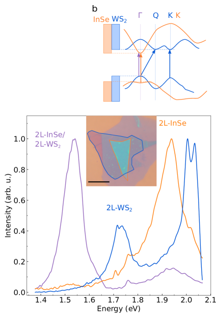
We perform photoluminescence (PL) measurements that allow the identification of spectral features in the light emitted by vdW interfaces originating from interlayer electron-hole recombination. The behavior representative of the systems that we have studied is illustrated in Fig. 1 and 2, with data measured on structures formed by bilayer InSe (2L-InSe) and bilayer WS2 (2L-WS2), assembled to enable separate measurements of the PL coming from the individual layers and from their interface (see Fig. 1(a) for a schematic of the 2L-InSe/2L-WS2 interface and Fig. 1(b) for the relevant aspects of the band structure). Lines of different color in Fig. 1(c) represent the PL measured at T = 5 K on 2L-WS2 (blue line), 2L-InSe (orange line), and on their interface (purple line), and can be readily interpreted in terms of the known band structure of the materials forming the interface (see the arrows in Fig. 1(b)). The PL spectrum of 2L-WS2 shows a (split) peak at approximately 2 eV originating from direct recombination of excitons and trions at the K-point, and a lower energy peak at 1.73 eV due to k-indirect recombination of electrons at the Q-point with holes at the -point, as expected.zhao_evolution_2013 ; zhao_origin_2013 In the 2L-InSe spectrum a peak at approximately 1.9 eV is present, corresponding to the so-called A-transition in this system.mudd_tuning_2013 ; mudd_high_2015 ; mudd_direct–indirect_2016 The vdW interface PL, in contrast, is dominated by a peak close to 1.55 eV, significantly lower than the energy of the peaks identified in the spectra of the constituent materials, without any pronounced feature corresponding to those of 2L-WS2 and 2L-InSe. We directly conclude that the interfacial PL cannot be explained in terms of intralayer transitions, and that the 1.55 eV peak originates from an interlayer transition resulting from charge transfer that quenches the PL of the individual layers.
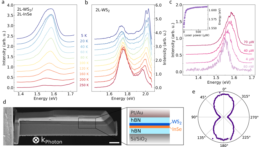
The temperature evolution of the interfacial PL intensity (Fig. 2a) and its dependence on the excitation laser power (Fig. 2c) do indeed exhibit the behavior characteristic of interlayer transitions that are direct in k-space. Fig. 2a shows that upon reducing T from 250 to 5 K, the intensity of the 1.55 eV PL peak steadily increases, as expected for a transition that is direct in k-space. For comparison, Fig. 2b shows that in 2L-WS2 the amplitude of the 2 eV peak originating from k-direct recombination at the K-point also increases upon cooling, whereas the amplitude of the 1.75 eV peak due to the k-indirect transition between the Q and the point decreases, as typical for phonon mediated processes. Upon increasing the excitation laser power, the transition energy increases by more than 50 meV before saturating as the power exceeds 100 W (see Fig. 2c and its inset). The blue-shift is a manifestation of the electrostatic potential generated by the “pumped” interlayer excitons, whose density increases (and eventually saturates) at higher excitation power. In simple terms, the photo-generated excitons consist of electrons residing in one layer (InSe) and of holes in the other layer (WS2), so that a higher exciton density results in a net electrostatic potential difference between the two layers and –owing to the interlayer nature of the transition– in a shift of the transition energy (as discussed extensively in the literature –see for instance butov_magneto-optics_1999 ; laikhtman_exciton_2009 – this interpretation in terms of an interlayer electrostatic potential difference is fully equivalent to accounting for the effect of the dipole-dipole interaction between the photo-excited excitons). In the same power range, a virtually identical behavior is observed in PL studies of interlayer excitons in vdW interfaces formed by MoSe2 and WSe2 monolayers,rivera_observation_2015 ; nagler_interlayer_2017 ; miller_long-lived_2017 but it is never observed in individual monolayers. We conclude that the transition responsible for the 1.55 eV line in the PL power spectrum of the 2L-InSe/2L-WS2 interface originates from an interlayer, k-direct transition, as expected for the - transition from the bottom of the conduction band of 2L-InSe to the top of the valence band of 2L-WS2.
One more direct experimental indication of the origin of the interlayer transition that we observe comes from the analysis of polarization of the emitted light. At the -point, the edge of the InSe conduction band and WS2 valence band consist of atomic orbitals whose angular momentum component in direction perpendicular to the plane is zero.brotons-gisbert_out–plane_2019 ; hamer_indirect_2019 Theoretically this prescribesterry_infrared–violet_2018 that the polarization of the photons emitted in the interlayer transition should be perpendicular to the interface. To check if this expectation is satisfied we fabricated dedicated devices –by cutting into a lamella configuration a block of 2 m x 20 m x 0.7 m out of h-BN encapsulated 2L-WS2/6L-InSe using a focused ion beam (see Fig. 2(d))– and measured the light emitted in the plane of the interface from the side of the lamella. The resulting polarization map is shown in Fig. 2(e), with a very pronounced out-of-plane photon polarization, as expected.
On the basis of experimental observations similar to those just presented for 2L-InSe/2L-WS2 interfaces, we conclude that also all other interfaces that we have investigated, based on combinations of thicker WS2 and InSe multilayers, exhibit direct interlayer transition at . The same is true for interfaces in which the WS2 multilayers are substituted by MoSe2, or MoS2. In all these systems, the PL spectrum of the interfaces exhibits a peak at an energy smaller than that of the spectral features of the individual constituent materials, whose amplitude increases upon cooling and whose frequency blue-shifts upon increasing the power of the exciting laser. The observed behavior is entirely consistent with the fact that all the semiconducting TMDs employed to assemble the interfaces have their valence band maximum centered at the -point, and the same is true for the conduction band minimum of all the InSe multilayers.butov_magneto-optics_1999 ; laikhtman_exciton_2009 ; rivera_observation_2015 ; nagler_interlayer_2017 Interestingly, the PL of the interfaces can be even brighter than that of the individual constituents, showing that interlayer - transitions can result in an increased efficiency for light emission (see Supplementary Information section S3).
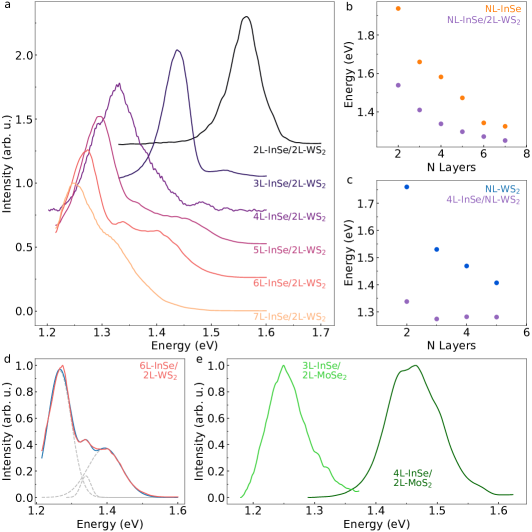
Figure 3 shows representative data reproduced in more than 40 structures that we have investigated experimentally. In Fig. 3a we show the evolution of the PL spectrum measured at T = 5 K on interfaces consisting of 2L-WS2 and of InSe multilayers of increasing thickness (from 2L to 7L), and in Fig. 3b we compare the thickness dependence of the interlayer transition energy extracted from Fig. 3a (purple dots) to the energy of the intralayer transition in the corresponding InSe multilayers (orange dots). As stated above, for all thicknesses the interlayer transition occurs at a lower energy than the intralayer one. A similar behavior is observed upon fixing the thickness of the InSe layer and varying that of the WS2 multilayers, as illustrated in Fig. 3c for interfaces consisting of 4L-InSe and NL-WS2, with N varying from 2 to 5. Data measured on interfaces based on InSe and semiconducting TMDs other than WS2 are presented in Fig. 3e. Fig. 3e shows the PL originating from interlayer electron-hole recombination in 3L-InSe/2L-MoSe2 and in 4L-InSe/2L-MoS2: for these materials we did not systematically study the evolution of the interlayer transition energy upon varying thickness, but we did measure several interfaces combining multilayers of different thickness, and observed in all cases PL (again, with an amplitude that increases upon lowering temperature, at an energy that blue-shifts upon increasing excitation laser power). However, for interfaces based on WSe2 and InSe we did not observe any PL signal, despite the expected presence of a k-direct interlayer transition at the -point. We believe that this is because the transition occurs at an energy of 0.8-0.9 eV, approaching the limit of sensitivity of our detector camera (the presence of a non-radiative recombination path that quenches the PL, e.g. due to material-specific impurities creating in-gap states, can not be entirely ruled out at this stage).
We conclude that k-direct interlayer transitions at are robust processes, as we have shown them to occur irrespective of the relative orientation of the multilayers forming the interface (in the majority of cases we did not align the crystals when assembling the structures), of a substantial lattice constant mismatch (approximatively 15 %) between the constituents, and despite the fact that the band structure of TMD multilayers changes significantly upon varying their thickness. Besides substantiating our initial strategy to engineer systems for broad-spectrum optoelectronics, the ability to detect interlayer transitions in so many different interfaces enables the relative optical band alignment of entire classes of materials to be determined quantitatively, in a rather straightforward and reproducible way. This is a significant result, because band offsets of semiconductors are often complex to measure precisely, and different techniques give different results depending on details of how experiments are done.
To understand how the alignment of the different band edges is determined, we discuss in detail the procedure for 2L-InSe/2L-WS2 interfaces, whose relevant band edges are represented in Fig. 4a. The interlayer transition occurring at 1.55 eV measures the distance in energy between the bottom of the 2L-InSe conduction band and the top of the 2L-WS2 valence band at the -point. The intralayer transition in 2L-InSe fixes the energy distance between the valence band maximum and the conduction band minimum (both near the -point) in this 2D semiconductor (approximately 1.93 eV). Similarly, the indirect intralayer transition in 2L-WS2 (approximately 1.73 eV) fixes the position of the bottom of the conduction band in bilayer WS2 at the Q-point, relative to the maximum of the valence band at . Since in 2L-WS2 the conduction band edge at the Q and K points are nearly degeneratenguyen_visualizing_2019 (the energy difference is at most a few tens of meV, which we neglect here), we can use the k-direct, 2.0 eV intralayer transition at K in 2L-WS2 to determine the energy of the maximum at K of the valence band of 2L-WS2. The relative alignment of all relevant band edges in 2L-InSe and 2L-WS2 is then entirely determined. The same holds true for all other layers that we have investigated: 2L-WS2 and InSe multilayers up to 7L-InSe (Fig. 4b), for 4L-InSe and WS2 of thickness increasing from 2L to 5L (Fig. 4c), and for 4L-InSe combined with all the different semiconducting TMDs (Fig. 4d). We estimate the precision of the band-gap values extracted from this procedure to be 100 meV or better. A source of uncertainty comes from neglecting the binding energy of interlayer excitons, which is justified because for all interfaces investigated in our work this quantity is significantly smaller than 100 meV (see Section S4 of the Supplementary Information). What also limits the precision of our analysis are the assumption that the conduction band edges at the K and Q points of 2L TMDs are energy degenerate (correct only within a few tens of meV), and having neglected hybridization effects between the valence band edges of InSe and TMD multilayers in which these edges are energetically aligned (based on previous studies of other vdW interfaces reported in the literature,wilson_determination_2017 we estimate the phenomenon to cause an indetermination of 50 meV or less).
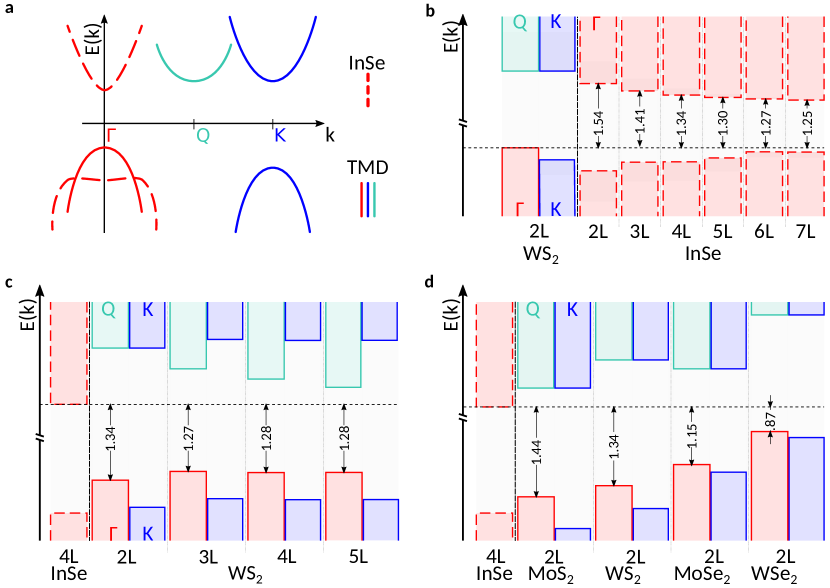
The internal consistency of the band diagrams extracted from the measured interlayer and intralayer transition energies can be cross-checked directly with the measured data. For instance, all measurements on interfaces formed by 2L-WS2 and NL-InSe shown in Fig. 3a were performed with the excitation laser tuned at the K-K transition of 2L-WS2. The photo-excited electron at the K-point of the 2L-WS2 conduction band has always enough energy to be transferred to the InSe multilayer (Fig. 4b), which is why the interlayer transition in the PL spectrum is visible. For 5L-InSe and thicker layers, in addition, the top of the 2L-WS2 K-valley becomes nearly degenerate with the top of the valence band of InSe at the -point, so that also the hole in the K-valley of 2L-WS2 can transfer into InSe. This has measurable consequences, since for 5L- and thicker InSe multilayers it leads to PL originating from the InSe intralayer transition, as well as to splitting of the transitions involving the -point valence band edge (due to hybridization of states in 2L-WS2 and in InSe). The PL spectra of 5L-, 6L-, and 7L-InSe (Fig. 3a) do indeed show multiple peaks, one of which is due to the intralayer transition in InSe, and another that we attribute to the hybridization-induced splitting (see Fig. 3d for the decomposition of the PL spectrum; a systematic discussion of hybridization effects will be presented elsewhere). Additional evidence in support of the band diagrams shown in Fig. 4 is obtained from PL energy spectroscopy –i.e., from measurements of the PL intensity as a function of the exciting energy of the photon– that we discuss in the supplementary information section S1. Finally, note also the different behavior of the band edges in InSe and WS2 multilayers (compare Fig. 4b and 4c): whereas in InSe both the conduction and valence band edges shift as thickness is increased (Fig. 4b), in WS2 the valence band edge remains nearly constant as the thickness is increased past that of bilayers (Fig. 4c) in agreement with existing Angle-Resolved Photoemission Spectroscopy (ARPES) experiments.wilson_determination_2017
Besides demonstrating the validity of the proposed strategy for the realization of vdW interfaces supporting k-direct transitions, the band diagrams in Fig. 4 show how the interfacial transition energy can be engineered by simply selecting different thicknesses of the most commonly available 2D materials. The heterostructures investigated here densely cover the interval between approximatively 1.0 and 1.6 eV, but a much larger interval can be spanned by employing other known materials. Bilayers or multilayers of MoTe2, and of GaSe, for instance, will allow the energy interval to be extended further on the lower and higher end, respectively. It is this versatility and physical robustness that makes the use of interfacial transitions at the -point ideally suited for the realization of broad spectrum optoelectronic applications. There is broad consensus that optoelectronics is one of the most promising domains for the development of devices based on interfaces of 2D materials, but the large-scale production and commercialization of such devices pose serious challenges as to the required level of material control. This is undoubtedly the case if device operation relies on a very fine control of the different constituents, such as a perfect alignment of 2D crystals, or combining materials with identical crystal lattices and lattice constants. While some of the challenges may be solved in the long term, these requirements are incompatible with virtually all large-area manufacturing techniques that are currently available. The results reported here, however, change the situation, since with an appropriate choice of materials vdW interfaces can be used as radiation sources covering a very broad frequency spectrum, in a mode of operation that is extremely robust against variations of interfacial structural details. This implies that even the simplest possible techniques to assemble large-area interfaces of atomically thin layers –such as liquid phase exfoliation followed by ink-jet printing– can be employed for the scalable fabrication of structures with useful optoelectronic functionality.
Methods
Sample fabrication. The fabrication of the heterostructures has been performed according to previous works (ref. ponomarev_semiconducting_2018 ) and reproduced here for completeness. The fabrication of the heterostructures used to perform the measurements discussed in the main text relies on conventional techniques that are commonly employed to manipulate atomically thin crystals, i.e., 2D materials. Atomically thin layers of TMDs and InSe are obtained by mechanical exfoliation of bulk crystals in a nitrogen gas filled glove box with a < 0.5 ppm concentration of oxygen and water; the TMD crystals are purchased from HQ graphene and the InSe orignate from a Bridgman-grown crystal of -rhombohedral InSe. The exfoliated crystals are transferred onto Si/SiO2 substrate and suitable flakes are identified by looking at their optical contrast under an optical microscope. The heterostructures are then assembled in the same glove box with a conventional pick-up and release technique based on either PPC/PDMS (Poly(propylene carbonate) /polydimethylsiloxane) or PC/PDMS (polycarbonate) polymer stacks placed on glass slides. The samples, encapsulated in between exfoliated h-BN crystals of few tens of nanometers, are removed from the glovebox and placed into the cryostat for optical investigations.
Optical measurements. Photoluminescence measurements in a backscattering geometry (illumination direction out-of-plane) are performed by using an optical microscope to illuminate the device with the incoming laser beam and to collect the resulting emitted light. The light source is a supercontinuum white light laser combined with a contrast filter, allowing to tune the laser wavelength between 400 and 1100 nm. The illumination wavelength for every spectrum is specified in the main text and the laser power kept at 50 , if not stated otherwise. All measurements are done with the sample placed in the vacuum chamber with a cryostat mounted on a piezoelectric driven x-y stage allowing positioning precision down to 50 nm (Cryovac KONTI). The laser beam is coupled onto the sample using an optical microscope with long working distance objectives producing a spot of approximately 1 m in diameter that can be focused anywhere on the sample surface. The light collected from the sample is sent to a Czerny-Turner monochromator with a grating of 150 gr/mm (Andor Shamrock 500i) and detected with a Silicon Charge Coupled Device (CCD) array (Andor Newton 970 EMCCD).
PL on lamella samples. The fabrication of the lamella samples has been performed according to previous works (ref. hamer_indirect_2019 ) and reproduced here for completeness. Heterointerfaces for investigation of the in-plane PL are obtained in a similar manner as described in sample fabrication. However, an additional layer of thick (>100 nm) h-BN is transferred on top of the encapsulated heterointerface, followed by 3 nm AuPd + 5 nm amorphous carbon to protect the sample from ion damage. An area for extraction is then identified using AFM and covered with an additional protective platinum mask (1 m thick) using a FEI Helios focused ion beam (FIB) dual-beam system. FIB milling is performed using a 30 kV Ga+ beam to extract the selected area. An OmniProbe micromanipulator is used to lift the lamella, rotate it by 90, and secure it onto an Omicron transmission electron microscopy grid. Finally, damaged edges of the lamella are polished by further FIB milling with a decreasing series of acceleration voltages (e.g. 5 kV, 47 pA and 2 kV, 24 pA). The final thickness of the specimen is <1 m, to suppress multiple internal reflections of the emitted light. The polarization measurements are taken at 4 K in an AttoDry 100 cryostat (AttoCFM inset), using Princeton Instruments Acton Spectrapro SP-2500i CCD with 300 gr/mm grating.
Acknowledgements
We gratefully acknowledge Alexandre Ferreira for continuous and precious technical support. AFM gratefully acknowledges financial support from the Swiss National Science Foundation (Division II) and from the EU Graphene Flagship project. NU gratefully acknowledges financial support from the Swiss National Science Foundation through the Ambizione program. RVG and VIF gratefully acknowledges financial support from European Graphene Flagship Core 2 Project under grant agreement 785219, ERC Synergy Grant Hetero2D, EPSRC grants EP/S030719/1, EP/S019367/1, EP/P026850/1 and EP/N010345/1, Lloyd Register Foundation Nanotechnology Grant. K.W. and T.T. acknowledge support from the Elemental Strategy Initiative conducted by the MEXT, Japan, A3 Foresight by JSPS and the CREST (JP-MJCR15F3), JST. ZDK acknowledges the support from the National Academy of Sciences of Ukraine
Author contributions
N.U., E.P., J.Z., and D.T. have equally contributed. AFM and VIF have conceived the idea of this project. N.U., E.P., D.T., D.D., J.Z., J.H., and I.G.L. fabricated heterostructures, participated in their characterization, and analyzed the data. D.T., J.Z., J.H., A.Z, and R.V.G. designed and performed the experiment on the lamella samples. V.Z. and V.I.F. developed the theory of optical transitions at in vdW interfaces. Z.R.K., Z.D.K., A.P., T.T., and K.W. provided InSe and h-BN crystals. N.U., E.P., R.V.G., V.I.F, and A.F.M wrote the manuscript with input from all authors. All authors discussed the results.
Competing financial interests
The authors declare no competing financial interests.
Data availability
The data that support the findings of this study are available from the corresponding authors without any restriction.
References
- (1) Geim, A. K. & Grigorieva, I. V. Van der Waals heterostructures. Nature 499, 419–425 (2013). URL https://www.nature.com/articles/nature12385.
- (2) Novoselov, K. S., Mishchenko, A., Carvalho, A. & Neto, A. H. C. 2d materials and van der Waals heterostructures. Science 353, aac9439 (2016). URL https://science.sciencemag.org/content/353/6298/aac9439.
- (3) Fang, H. et al. Strong interlayer coupling in van der Waals heterostructures built from single-layer chalcogenides. Proceedings of the National Academy of Sciences 111, 6198–6202 (2014). URL https://www.pnas.org/content/111/17/6198.
- (4) Rivera, P. et al. Interlayer valley excitons in heterobilayers of transition metal dichalcogenides. Nat. Nanotechnol. 13, 1004 (2018). URL https://www.nature.com/articles/s41565-018-0193-0.
- (5) Castellanos-Gomez, A. et al. Local Strain Engineering in Atomically Thin MoS2. Nano Lett. 13, 5361–5366 (2013). URL https://doi.org/10.1021/nl402875m.
- (6) Rivera, P. et al. Observation of long-lived interlayer excitons in monolayer MoSe2-WSe2 heterostructures. Nat. Commun. 6, 6242 (2015). URL http://www.nature.com/doifinder/10.1038/ncomms7242.
- (7) Ross, J. S. et al. Interlayer Exciton Optoelectronics in a 2d Heterostructure p-n Junction. Nano Lett. 17, 638–643 (2017). URL https://doi.org/10.1021/acs.nanolett.6b03398.
- (8) Mennel, L., Paur, M. & Mueller, T. Second harmonic generation in strained transition metal dichalcogenide monolayers: MoS2, MoSe2, WS2, and WSe2. APL Photonics 4, 034404 (2018). URL https://aip.scitation.org/doi/full/10.1063/1.5051965.
- (9) Ciarrocchi, A. et al. Polarization switching and electrical control of interlayer excitons in two-dimensional van der Waals heterostructures. Nat. Photonics 13, 131 (2019). URL https://www.nature.com/articles/s41566-018-0325-y.
- (10) Yu, H., Wang, Y., Tong, Q., Xu, X. & Yao, W. Anomalous Light Cones and Valley Optical Selection Rules of Interlayer Excitons in Twisted Heterobilayers. Phys. Rev. Lett. 115, 187002 (2015). URL https://link.aps.org/doi/10.1103/PhysRevLett.115.187002.
- (11) Lee, C.-H. et al. Atomically thin p–n junctions with van der Waals heterointerfaces. Nat. Nanotechnol. 9, 676–681 (2014). URL https://www.nature.com/articles/nnano.2014.150.
- (12) Furchi, M. M., Pospischil, A., Libisch, F., Burgdörfer, J. & Mueller, T. Photovoltaic Effect in an Electrically Tunable van der Waals Heterojunction. Nano Lett. 14, 4785–4791 (2014). URL https://doi.org/10.1021/nl501962c.
- (13) Mueller, T., Pospischil, A. & Furchi, M. M. 2d materials and heterostructures for applications in optoelectronics. In Micro- and Nanotechnology Sensors, Systems, and Applications VII, vol. 9467, 946713 (International Society for Optics and Photonics, 2015). URL https://www.spiedigitallibrary.org/conference-proceedings-of-spie/9467/946713/2D-materials-and-heterostructures-for-applications-in-optoelectronics/10.1117/12.2176848.short.
- (14) Binder, J. et al. Upconverted electroluminescence via Auger scattering of interlayer excitons in van der Waals heterostructures. Nat. Commun. 10, 2335 (2019). URL https://www.nature.com/articles/s41467-019-10323-9.
- (15) Zhu, H. et al. Interfacial Charge Transfer Circumventing Momentum Mismatch at Two-Dimensional van der Waals Heterojunctions. Nano Lett. 17, 3591–3598 (2017). URL https://doi.org/10.1021/acs.nanolett.7b00748.
- (16) Ponomarev, E., Ubrig, N., Gutiérrez-Lezama, I., Berger, H. & Morpurgo, A. F. Semiconducting van der Waals Interfaces as Artificial Semiconductors. Nano Lett. 18, 5146–5152 (2018). URL https://doi.org/10.1021/acs.nanolett.8b02066.
- (17) Splendiani, A. et al. Emerging Photoluminescence in Monolayer MoS2. Nano Lett. 10, 1271–1275 (2010). URL http://dx.doi.org/10.1021/nl903868w.
- (18) Mudd, G. W. et al. Tuning the Bandgap of Exfoliated InSe Nanosheets by Quantum Confinement. Adv. Mater. 25, 5714–5718 (2013). URL https://onlinelibrary.wiley.com/doi/abs/10.1002/adma.201302616.
- (19) Bandurin, D. A. et al. High electron mobility, quantum Hall effect and anomalous optical response in atomically thin InSe. Nat. Nanotechnol. 12, 223–227 (2017). URL https://www.nature.com/articles/nnano.2016.242.
- (20) O. Göbel, E. & Ploog, K. Fabrication and optical properties of semiconductor quantum wells and superlattices. Prog. Quantum Electron. 14, 289–356 (1990). URL http://www.sciencedirect.com/science/article/pii/007967279090001E.
- (21) He, L. et al. MBE growth of (111) CdTe on Zn-stabilized and Se-stabilized (100) ZnSe. J. Cryst. Growth 101, 147–152 (1990). URL http://www.sciencedirect.com/science/article/pii/002202489090954J.
- (22) O’Donnell, K. P. & Henderson, B. The Zn(Cd)S(Se) family of superlattices. J. Lumin. 52, 133–146 (1992). URL http://www.sciencedirect.com/science/article/pii/0022231392902396.
- (23) Yu, E. T., McCaldin, J. O. & McGill, T. C. Band Offsets in Semiconductor Heterojunctions. In Ehrenreich, H. & Turnbull, D. (eds.) Solid State Physics, vol. 46, 1–146 (Academic Press, 1992). URL http://www.sciencedirect.com/science/article/pii/S0081194708603975.
- (24) Butov, L. V., Imamoglu, A., Mintsev, A. V., Campman, K. L. & Gossard, A. C. Photoluminescence kinetics of indirect excitons in GaAs/AlxGa1-xAs coupled quantum wells. Phys. Rev. B 59, 1625–1628 (1999). URL https://link.aps.org/doi/10.1103/PhysRevB.59.1625.
- (25) Kroemer, H. Nobel Lecture: Quasielectric fields and band offsets: teaching electrons new tricks. Rev. Mod. Phys. 73, 783–793 (2001). URL https://link.aps.org/doi/10.1103/RevModPhys.73.783.
- (26) Klingshirn, C. F. Semiconductor Optics. Graduate Texts in Physics (Springer-Verlag, Berlin Heidelberg, 2012), 4 edn. URL https://www.springer.com/gp/book/9783642283611.
- (27) Butov, L. V. Excitonic devices. Superlattices Microstruct. 108, 2–26 (2017). URL http://www.sciencedirect.com/science/article/pii/S0749603616316561.
- (28) Zhao, W. et al. Evolution of Electronic Structure in Atomically Thin Sheets of WS2 and WSe2. ACS Nano 7, 791–797 (2013). URL http://dx.doi.org/10.1021/nn305275h.
- (29) Zhao, W. et al. Origin of Indirect Optical Transitions in Few-Layer MoS2, WS2, and WSe2. Nano Lett. (2013). URL http://pubs.acs.org/doi/abs/10.1021/nl403270k.
- (30) Mudd, G. W. et al. High Broad-Band Photoresponsivity of Mechanically Formed InSe–Graphene van der Waals Heterostructures. Adv. Mater. 27, 3760–3766 (2015). URL https://www.onlinelibrary.wiley.com/doi/abs/10.1002/adma.201500889.
- (31) Mudd, G. W. et al. The direct-to-indirect band gap crossover in two-dimensional van der Waals Indium Selenide crystals. Sci. Rep. 6, 39619 (2016). URL https://www.nature.com/articles/srep39619.
- (32) Butov, L. V., Shashkin, A. A., Dolgopolov, V. T., Campman, K. L. & Gossard, A. C. Magneto-optics of the spatially separated electron and hole layers in GaAs/AlxGa1-xAs coupled quantum wells. Phys. Rev. B 60, 8753–8758 (1999). URL https://link.aps.org/doi/10.1103/PhysRevB.60.8753.
- (33) Laikhtman, B. & Rapaport, R. Exciton correlations in coupled quantum wells and their luminescence blue shift. Phys. Rev. B 80, 195313 (2009). URL https://link.aps.org/doi/10.1103/PhysRevB.80.195313.
- (34) Nagler, P. et al. Interlayer exciton dynamics in a dichalcogenide monolayer heterostructure. 2D Mater. 4, 025112 (2017). URL https://doi.org/10.1088%2F2053-1583%2Faa7352.
- (35) Miller, B. et al. Long-Lived Direct and Indirect Interlayer Excitons in van der Waals Heterostructures. Nano Lett. 17, 5229–5237 (2017). URL https://doi.org/10.1021/acs.nanolett.7b01304.
- (36) Brotons-Gisbert, M. et al. Out-of-plane orientation of luminescent excitons in two-dimensional indium selenide. Nat. Commun. 10, 3913 (2019). URL https://www.nature.com/articles/s41467-019-11920-4.
- (37) Hamer, M. J. et al. Indirect to Direct Gap Crossover in Two-Dimensional InSe Revealed by Angle-Resolved Photoemission Spectroscopy. ACS Nano 13, 2136–2142 (2019). URL https://doi.org/10.1021/acsnano.8b08726.
- (38) Terry, D. J. et al. Infrared-to-violet tunable optical activity in atomic films of GaSe, InSe, and their heterostructures. 2D Mater. 5, 041009 (2018). URL http://stacks.iop.org/2053-1583/5/i=4/a=041009.
- (39) Nguyen, P. V. et al. Visualizing electrostatic gating effects in two-dimensional heterostructures. Nature 572, 220–223 (2019). URL https://www.nature.com/articles/s41586-019-1402-1.
- (40) Wilson, N. R. et al. Determination of band offsets, hybridization, and exciton binding in 2d semiconductor heterostructures. Sci. Adv. 3, e1601832 (2017). URL https://advances.sciencemag.org/content/3/2/e1601832.