Ballistic Metamaterials
The interaction of free electrons with electromagnetic excitation is the fundamental mechanism responsible for ultra-strong confinement of light Cai2009 that, in turn, enables biosensing, near-field microscopy,NFM optical cloaking,cloaking-proposal-Pendry ; cloaking-proposal-Leonhardt ; cloaking-expt ; cloaking-optical sub-wavelength focusing,hyper-focusing-Viktor ; hyper-focusing-expt ; Natasha and super-resolution imaging.Pendry2000 ; hyperlensEN ; hyperlensNE ; hyperlens-Zhang ; hyperlens-3D These unique phenomena and functionalities critically rely on the negative permittivity of optical elements negative-refraction-expt resulting from the free electrons. As result, progress in nanophotonics and nano-optics is often related to the development of new negative permittivity (plasmonic) media at the optical frequency of interest.Cai2009 Here we show that the essential mobility of free charge carriers in such conducting media dramatically alters the well-known optical response of free electron gases. We demonstrate that a ballistic resonance associated with the interplay of the time-periodic motion of the free electrons in the confines of a sub-wavelength scale nanostructure and the time periodic electromagnetic field leads to a dramatic enhancement of the electric polarization of the medium – to the point where a plasmonic response can be achieved in a composite material using only positive bulk permittivity components. This ballistic resonance opens the fields of plasmonics, nanophotonics, and metamaterials to many new constituent materials that until now were considered unsuitable for such applications, and extends the operational frequency range of existing materials to substantially shorter wavelengths. As a proof of concept, we experimentally demonstrate that ballistic resonance in all-semiconductor metamaterials results in strongly anisotropic (hyperbolic) response well above the plasma frequencies of the metamaterial components.
These ballistic semiconductor metamaterials offer a practical path to leverage the maturity of the semiconductor industry to revolutionize photonics and optoelectronics. Furthermore, since the ballistic resonance, theoretically predicted and experimentally demonstrated in the present work using an all-semiconductor metal/dielectric materials system, is fundamentally different from the effect of inter-subband transitions in quantum wells – these two effects can be combined within the same material platform to further enhance the electromagnetic response as well as incorporate active components, and thus offer even more control over the optical properties of the resulting composite. Finally, the effect demonstrated here in planar layered metamaterials can be extended to other confined geometries, including wire- and particle-based nanostructures and composites.
Ballistic Resonance
The optical response of a wide class of materials that includes metals, semi-metals, transparent conducting oxides, and doped semiconductors, is dominated by the dynamics of their free electrons. In a composite (meta)material that include both conducting and dielectric constituents, the resulting free carrier contribution to the electromagnetic response of the system is defined by the relation of the electron de Broglie wavelength at the Fermi energy and the characteristic dimensions of the metallic component of the metamaterial unit cell .
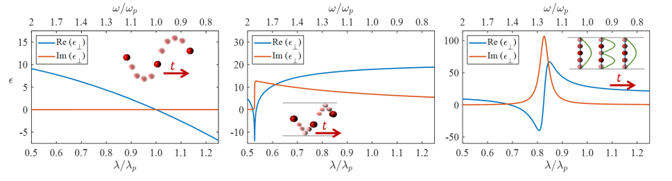
When is comparable to , the free electron motion in the conducting elements of the metamaterial unit cell is strongly quantized,ref:quantum leading to the characteristic Lorenzian profile (see Fig. 1(c)) centered at the frequency of the corresponding quantum transition between different energy levels. In particular, a planar metamaterial operating in the regime is essentially a multiple quantum well system, with the resonances in the effective permittivity corresponding to the electronic inter-subband transitions.QCL ; sinclair ; genevet ; zayatsNb
In the opposite limit , the quantum interference effects can be neglected, and the free electron response is generally treated within the framework of the standard Drude model,Cai2009 leading to the effective local permittivity
| (1) |
where is the corresponding plasma frequency and is the free electron scattering time, while represents the contribution of the bound electrons. The characteristic frequency dependence of is shown in Fig. 1(a).
However, in the semiclassical regime , the actual dynamics of the free electrons can be either diffusive Ziman ; ZimanP – when each electron undergoes multiple collisions before reaching the metal-dielectric interface, or ballistic ZimanP ; Datta when the electron mean free path . In the diffusive regime,ZimanP the standard description in terms of the local dielectric permittivity is generally adequate,hyperlensEN and the finite unit cell size corrections can be incorporated via the spatial dispersion formalism.LL ; Viktor The ballistic regime, on the other hand, shows qualitatively different behavior, with the resonant response due to the interplay of the electromagnetic field period and the ballistic round-trip time , where is the Fermi electron velocity. As we show in the present work, when the round-trip time of the electron motion is equal to the period of the electric field, the resulting electromagnetic response is enhanced, leading to the negative effective permittivity in the direction normal to the metal-dielectric interface, even above the plasma frequency when the corresponding bulk permittivity is positive – see Fig. 1(b). Note that this ballistic resonance does not involve the quantum interference of the electron de Broglie waves, and is therefore qualitatively different from the inter-subband oscillations in quantum wells.
To uncover the key features of (meta-)material response in the ballistic regime, we will focus on the planar geometry of Fig. 2(a). In this case the confinement primarily affects the motion of electrons in the direction that is perpendicular to the interface, and the effective permittivity of the conducting layer becomes anisotropic (see Methods for details). For a high-quality interface when the free electron is reflected from the boundary with essentially the same in-plane component of its momentum, the electromagnetic response along the layer can be represented by the effective permittivity that is still described by the conventional Drude model,
| (2) |
However, as the reflection from the interface inevitably changes the normal component of the electron velocity, in the direction normal to the interface the free carrier electromagnetic response is strongly modified. When the layer is substantially thick (), the effective permittivity in the direction perpendicular to the layer can be calculated using the semiclassical approach, based on the self-consistent solution of the Boltzmann kinetic equation Ziman for the charge carrier distribution function in the layer, in the electromagnetic field defined by Maxwell’s equations with charge and current densities that, in turn, depend on the electron distribution function ZimanP (see Appendix C), resulting in
| (3) |
where is the Fermi velocity of electrons and the function is defined as
| (4) |
giving a logarithmic singularity in the low-loss limit when for an integer , corresponding to the ballistic resonance. Fig. 1(b) shows the resulting frequency dependence of the effective permittivity normal to the layer . Note the difference of the frequency profile of the ballistic resonance from the usual Lorentzian shape: here it’s the real part of the permittivity which peaks at the resonance, while the imaginary component which accounts for loss, rapidly drops to near-zero in a step-like fashion (see Appendix F).
The physical origin of the non-zero imaginary part of the permittivity in the low-loss limit is the Landau damping.LL For simplicity, consider the frequencies near the primary () ballistic resonance (). There, an electron with the velocity exhibits periodic motion in the direction (normal to the interface), with temporal period equal to that of the electromagnetic field. As a result, such a free electron moves “in phase” with the electromagnetic field, and can therefore continuously absorb the field’s energy. For a degenerate Fermi gas, has to be below the Fermi velocity , so that such in-phase motion is only possible when , i.e. only at the frequencies below but not above the ballistic resonance – which explains the asymmetric absorption profile.
When the layer thickness , the semiclassical approach becomes inadequate and the optical response should be based on full quantum-mechanical calculations. In the limit of ultra-thin layers, the optical response is dominated by discrete quantum well transitions, recovering the expected Lorentzian line shapes (Fig.1c). Importantly, the results of full quantum-mechanical calculations agree with predictions of semiclassical theory for relatively thick layers. Likewise, semiclassical theory predicts as .
The approach derived in this section is also directly applicable to curved layers as long as the radius of curvature is much larger that the layer thickness , and it can be re-formulated to describe optical properties of wires and nanoparticles of various shapes. In the latter case, we expect the results to be shape-dependent.
Ballistic metamaterials
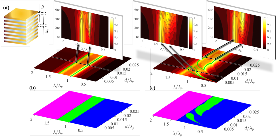
To demonstrate the effect of the ballistic resonance for designing the optical properties of complex composites, we consider the planar metamaterial, where the free electron gas is confined to the conducting layers with the width , surrounded by undoped dielectric “barriers” of thickness (see the schematics in Fig.2(a)). In the limit , the multilayer metamaterial behaves as a homogeneous media with uniaxial dielectric permittivity tensor related to permittivities of its components (see Appendix D) via Viktor
| (5) |
Depending on the relative sign of and , the optical response of the metamaterial resembles that of a uniaxial transparent dielectric (), an anisotropic reflective metal (), or the strongly anisotropic media commonly referred to as a hyperbolic material () which is able to support the propagation of strongly confined waves and has been demonstrated to be a flexible platform for subwavelength focusing hyper-focusing-Viktor ; hyper-focusing-expt , imaging hyperlensEN ; hyperlensNE ; hyperlens-Zhang ; hyperlens-3D , and lifetime and emission manipulation.ZJISEN ; NoginovQED ; ShalaevQED Note that in all previous realizations of hyperbolic metamaterials, the constituent metallic layers have been assumed to operate in the Drude regime.
The ballistic resonance has profound implications for the electromagnetic response of planar metamaterials. Even if the system is operated at frequencies well above the plasma resonance () such that all constituents of the metamaterial show positive bulk permittivities (, ), near the ballistic resonance , so that the composite behaves as a hyperbolic metamaterial. This offers unprecedented potential in the design and fabrication of plasmonic and hyperbolic metamaterials that do not need any negative-permittivity components.
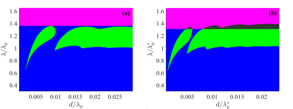
Fig. 2 shows the phase diagrams of the planar metamaterial with using the conventional Drude approach and the ballistic model discussed in this work. Here we see the contrast between the conventional effective medium approach that ignores the inherent mobility of the free charge carriers (panel (b) and the actual behavior (panel (c)).
In the framework of the effective-medium theory with the local (Drude) permittivities,ref:nmat ; Viktor the phase diagram only shows three different “phases” of the electromagnetic response of the metamaterial: the dielectric phase with (blue color in Fig. 2), the type-I hyperbolic phase ref:Zubin-types with , (green color in Fig. 2), and the type-II hyperbolic phase ref:Zubin-types with , (magenta color in Fig. 2). Note that in the local theory, the boundaries between different “phases” do not depend on the layer thickness (as long as the system is within the metamaterial limit ) – see Fig. 2(b).
However, the actual phase diagram (see Fig. 2(c)) is substantially different from this comparatively simple behavior. For a relatively large value of the layer thickness (so that ), the system is in the diffusive regime, and its evolution with a change in the frequency is similar to the predictions of the local theory – see Fig. 2(b). However, even in this diffusive regime there are visible differences in the phase diagrams. Now, two topologically different hyperbolic phases are no longer connected, but instead separated from each other by a narrow region of the dielectric response – see Fig. 2(c). Furthermore, the frequencies of the phase transitions that define the phase boundaries of the type-I hyperbolic phase (represented by the green color in the phase diagrams) now nontrivially depend on the layer thickness. This is a direct consequence of the ballistic resonance, whose signatures are already apparent even in the diffusive regime. Close to the resonance, the free carrier response is enhanced, and the resulting hyperbolic behavior is extended to higher frequencies. However, due to the general properties of periodic resonant response, the resonance frequencies of different orders are separated by “anti-resonances” of the reduced response, similar to the constructive and distructive interference in wave phenomena. Close to these “anti-resonances”, the free-carrier response is suppressed, and the frequency bandwidth of the type-I hyperbolic phase is reduced below the range that is expected from the local theory – see Fig. 2(c).
At smaller layer thickness (corresponding to lower orders in the ballistic resonance condition ) the ballistic effects become progressively stronger, with increasingly broader frequency range of the hyperbolic response on-resonance and reduced bandwidth at anti-resonance, leading to a complete separation of the hyperbolic phase for into an “island” in the phase diagram of Fig. 2(b), and the type-II hyperbolic phase (magenta color in Fig. 2). Defined by the zero-order ballistic resonance, this island of type-I hyperbolic response follows the line of at progressively higher frequencies, well above the plasma frequency – see Fig. 2(c). Indeed, the hyperbolic phase now extends to frequencies that substantially exceed the plasma frequency of the conducting layers.
For the semiclassical description to apply in the ballistic regime, the layer thickness should exceed the electron de Broglie wavelength at the Fermi energy , while at the same time be on the order of or smaller than the electron mean free path and the characteristic electron displacement per single electromagnetic period , which implies that
| (6) |
where is the Fermi velocity. The inequality (6) can be expressed in terms of the carrier density as
| (7) |
Depending on the background dielectric permittivity (that excludes the contribution of free carriers) and the free carrier effective mass, Eqn. (7) leads to for a semiconductor from the III-V family such as a gallium arsenide ref:nmat (, ), to in conducting oxides such as ITO ITO (, ), and to for plasmonic metals such as gold or silver AlexModels (, ). For the semiconductor - based metamaterials ref:nmat studied in our experiments, the characteristic doping level is at the level of , and the semiclassical criterion of (7) is therefore well satisfied. In plasmonic metals, the actual free electron densities at the level of also substantially exceed the corresponding critical value of , . On the other hand, for conducting oxides the free carrier density is on order of , which is relatively close to the corresponding value of . As a result, the semiclassical regime, while relatively limited in the metamaterials based on transparent conducting oxides, dominates the response of semiconductor and high-quality single-crystal metal-dielectric metamaterials.
However, in absolute terms the ballistic resonance imposes substantially more stringent requirements on the fabrication quality of metal-dielectric composites than on that of the semiconductor metamaterials. Ballistic resonance is rapidly suppressed by the diffuse surface scattering of the free electrons, when the characteristic interface roughness exceeds the electron de Broglie wavelength . In a plasmonic metal, the latter is on the order of the inter-atomic distance – so for the ballistic resonance in a metal-dielectric composite one needs atomic level fabrication accuracy. In contrast to this behavior, the de Broglie wavelength in a semiconductor “designer metal” is on the order of - nm, so interface roughness well under a nanometer typical for semiconductor metamaterials (e.g. nm in high-quality GaInAs/AlInAs quantum-cascade structures Tsujino ), will have little effect on the ballistic resonance.
Topological transitions in Ballistic Metamaterials
As seen in Fig.2, for fixed values of the layer thicknesses, our planar metamaterial exhibits a series of topological transitions between elliptical, hyperbolic, or metallic phases as a function of operating frequency. Each of these transitions has a clear signature in the angle-resolved absorption spectra of the composite. Indeed, the high-frequency transition from elliptic into type-I hyperbolic phase is associated with an absorption resonance that monotonically increases as a function of incident angle (see Appendix A). At the same time, the transition into the type-II hyperbolic phase is associated with an absorption resonance that monotonically decays as a function of incident angle.
Importantly, only -polarized light is affected by these topological transitions, since the propagation of -polarized light only depends on . Therefore, a direct observation of the angle-enhanced absorption peak that is only present in the -polarized response of a planar metamaterial, at a frequency that substantially exceeds the value of (which can be measured independently), offers a clear and unambiguous signature of the hyperbolic band induced by the ballistic resonance.
While the origin of the ballistic resonance lies in the semiclassical dynamics of the system, the observed behavior is consistent with a full quantum description of the metamaterial. In a sense, the ballistic response describes a transition of the behavior of relatively thick “quantum” wells with large number of energy levels towards their infinitely thick counterparts, where electrons are best described as free carriers. Fig.3 illustrates the comparison between the topological phase diagram of the same metamaterial, as predicted by semiclassical theory and by full quantum mechanical calculations of the optical response of the metamaterial. Note that the semiclassical theory provides reasonable agreement with the full quantum solutions even in the limit of ultra-thin layers.
Experimental Results
For the experimental demonstration of the ballistic metamaterials and the associated resonance, III-V semiconductors offer several important advantages. First, as we will show in the subsequent analysis, this material platform ref:nmat offers a broad range of the system parameters (such as e.g. the doping density, or the material composition in the AlGaInAs alloys) that supports the semiclassical regime that lies in the heart of the ballistic resonance. In particular, epitaxially-grown III-V alloys allow for doping concentrations high enough for the semiconductor to behave as a plasmonic material at infrared wavelengths.Law2012 Second, III-V alloys offer high-quality, low material loss composites with near-atomic quality interfaces.ref:nmat The high quality of the interface is essential for ballistic metamaterials, as diffuse surface scattering will quickly suppress the ballistic resonance. Finally, with this choice the resulting metamaterials can share the same material platform with existing optoelectronic devices, which will greatly facilitate the introduction of such metamaterial elements into practical nanophotonic devices.
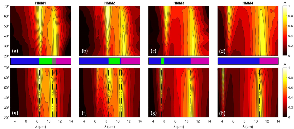
For the experimental demonstration of the ballistic metamaterials, we therefore use the “designer metal” semiconductor platform ref:nmat where the free electron gas results from the controllable doping of InGaAs layers, surrounded by undoped InAlAs dielectric “barriers” (see the schematics in Fig.2(a)). Our semiconductor metamaterial samples were grown lattice-matched to semi-insulating (100) InP substrates and consist of periods of alternating InGaAs and undoped InAlAs layers of equal thickness (). We have grown and characterized four metamaterial samples with decreasing period (): HMM1 ( nm), HMM2 ( nm), HMM3 ( nm), and HMM4 ( nm). All four samples were grown to have total HMM thickness of approximately 4 m. The details of the sample fabrication are described in Appendix A.
The doping concentration in our samples was determined by first growing bulk ( nm) - doped InGaAs layers on InP substrates. These bulk, highly doped InGaAs layers were characterized by IR reflection spectroscopy and the resulting spectra fitted using a transfer matrix method approach with the InGaAs modelled as a Drude metal, with plasma wavelength () and scattering rate () as fitting parameters. This approach of independent determination of the material parameters from experiments on the bulk samples allowed us to perform a direct comparison of our theoretical results to the measurements of transmission and reflection from the semiconductor metamaterials HMM1, HHM2, HHM3 and HHM4 with no additional fitting parameters.
The as-grown metamaterial samples HMM1, HHM2, HHM3 and HHM4 were characterized by angle- and polarization- dependent reflection and transmission spectroscopy using a Fourier transform infrared (FTIR) spectrometer with a custom built external reflection/transmission set-up. The details of the sample characterization and the transmission/reflection measurements are described in Appendix A.
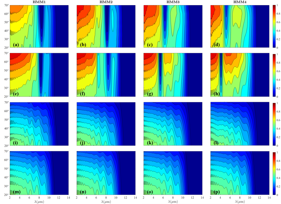
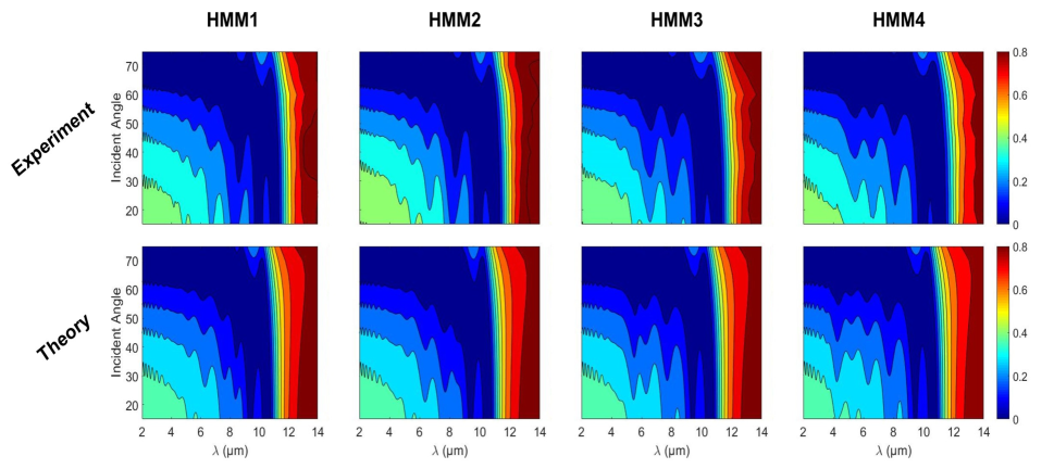
In Figs. 4 and 6 we present the comparison of the experimental data for the absorption (Fig. 4) and transmission (Fig. 6) with the corresponding theoretical results. Here, the theoretical calculation includes both the finite value of the conduction band offset between the InGaAs and AlInAs layers and the band nonparabolicity that becomes substantial at high doping densities. Note the quantitative agreement between the theory and the experimental data, with no fitting parameters.Note1
The “smoking gun” of the ballistic metamaterial behavior is the (single) transmission dip and the corresponding absorption peak at the wavelength that is well below the value of plasma wavelength of the material(s) forming the composite, as seen in Fig.6 and in Fig.4. As expected, our transmission data show well-defined transmission dips at the wavelengths of 8.53 m (HMM1), 8.25 m (HMM2), 6.35 m (HMM3), and 5.25 m (HMM4), which correspond to factors 0.996 (HMM1), 1.03 (HMM2), 1.34 (HMM3) and 1.62 (HMM4) smaller than the plasma wavelength (8.5 m) of the conducting layers.
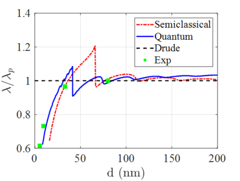
Fig.5 summarizes these trends by overlapping the experimental data with predictions of both full-quantum and semiclassical theories. The small deviation between the results of the semiclassical and quantum theories shown in Fig. 5, is due to band non-parabolicity that is taken into account in our quantum mechanical model but that is neglected by the semiclassical description. Most importantly, our experimental data are in quantitative agreement with both theoretical calculations - without the use of any fitting parameters. The increasing blueshift of the measured absorption features align with the signature of the topological transition predicted in our theory and provide conclusive evidence for the ballistic regime in semiconductor metamaterials.
The Discussion and Conclusions
In this work we introduced a new approach to designing the optical response of conducting nanostructures that takes advantage of the inherent mobility of the free electrons in conducting elements of the metamaterial unit cell. We have predicted the phenomenon of ballistic resonance, that leads to the negative dielectric permittivity well above the bulk plasma frequency of the bulk material. Our experimental data offer a direct observation of this new physical phenomenon in multilayered metamaterial, when a composite formed entirely from “dielectric” () materials, shows hyperbolic behavior.
The ballistic approach to optical metamaterials introduced in our work can therefore dramatically extend the application range of non-metallic material platforms, and open the field of nanophotonics and nanoplasmonics to materials that until now were considered unsuitable for such applications. In particular, the hyperbolic response of the planar semiconductor metamaterials above the plasma frequency of its highly-doped component, demonstrated in our experiments, shows that the use of these composites, originally introduced as “designer metals” for mid- and far-infrared frequencies,ref:nmat can now be extended closer to their interband absorption edge in the near-IR range. Our analysis suggests that similar phenomena are expected in noble metal platforms, potentially pushing these platforms into UV frequencies.
Finally, the ballistic resonance presented in this work is expected to play important role in the design of nanostructures with different geometries, including nanowire and nanoparticles, as well as on nanowire- and nanoparticle-composites.
Acknowledgements
This work was partially supported by the National Science Foundation grants DMR-1629276, DMR-1629330, and DMR-1629570, and by Gordon and Betty Moore Foundation.
Appendix A Sample Fabrication and Characterization
The hyperbolic metamaterial samples investigated in this work were grown by molecular beam epitaxy (MBE) in a Varian Gen II system with a valved arsenic cracker and effusion sources for gallium, indium and the silicon dopant. All samples were grown lattice-matched to semi-insulating (100) InP substrates and consist of multiple periods of alternating InGaAs and InAlAs layers of equal thickness nm (sample HMM1), nm (sample HMM2), nm (sample HMM3), and nm (sample HMM4). In all metamaterial samples, the total thickness of the hyperbolic multilayer was m.
The doping concentration was independently determined by first growing bulk (500 nm) - doped InGaAs layers on InP substrates. The bulk, highly doped InGaAs layers were characterized by IR reflection spectroscopy and the resulting spectra fitted using a transfer matrix method approach with the n++ InGaAs modeled as a Drude metal, which lead to the effective plasma wavelength of m and the scattering time of of ps. In addition, Hall measurements were used to determine the doping concentration of the of the bulk InGaAs ( cm-3), and it is this carrier concentration which was used for the numerical simulations modeling the optical behavior of the HMMs studied in this work.
Samples were characterized by angle- and polarization-dependent Fourier transform infrared (FTIR) reflection and transmission spectroscopy). Light from the internal FTIR source was collimated using two sequential apertures with diameters of approximately mm. A wire grid polarizer between the apertures was used to control the polarization of the incident light. The sample was mounted on a rotational stage with axis of rotation through the sample. For transmission experiments, transmitted light was collected by a reflective parabolic lens and focused onto a liquid nitrogen cooled HgCdTe (MCT) detector. The sample was rotated and spectra were collected for each polarization (TE and TM). All transmission spectra were normalized to the spectra collected with no sample in the beam path. For reflection measurements, the collecting lens and detector were rotated about the samples’ axis of rotation and positioned to collect the specular reflection from the sample. All reflection spectra are normalized to the reflection from a gold mirror, which in the mid-IR has near unity reflectivity for the angles and polarizations investigated.
Appendix B The effective medium theory
In the framework of the effective medium theory, the normal () and the tangential () components of the effective permittivity tensor of the conducting layer can be defined as
| (8) |
where is the free electrons’ polarization induced in the conducting layer in response to the electric field , and the brackets represent the average over the thickness of the conducting layer :
| (9) |
Alternatively, the normal component of the effective permittivity can be defined in terms of the ratio of the average field in the layer to the field at its boundary :
| (10) |
When the field in the conducting layer and the free electron polarization satisfy Gauss’s law
| (11) |
the two definitions of the effective permittivity (8) and (10) are equivalent to each other.
The problem of finding the electromagnetic response of a metamaterial in the ballistic regime therefore reduces to the task of finding the polarization of a single conducting layer in the external field.
Appendix C Semiclassical approach.
In the semiclassical approximation, the free carrier response can be treated within the semiclassical framework, via the Boltzmann kinetic equation Ziman :
| (12) |
where is the charge carriers’ distribution function with its equilibrium (Fermi-Dirac) limit , is the electron energy for the (Bloch) momentum , is the corresponding electron group velocity, and is the effective relaxation time defined by the bulk scattering (due to e.g. phonons, impurities, etc.) The local equilibrium distribution function is defined by the actual time-dependent local density rather than its time-averaged value,KraglerThomas1980 if the scattering process does not locally create or annihilate charge carriers. However, when the electromagnetic field frequency , the local correction to the equilibrium distribution function can be neglected.KliewerFuchs1968 ; MelykHarrison1970
For a high-quality interface along one of the symmetry planes of the crystal, the surface leads to specular reflection of the charge carriers,Ziman which can be accounted for by the boundary condition on the distribution function, Ziman ; Fuchs1938 ; ReuterSondheimer1948 ; Sondheimer1950 ; Soffer1967
| (13) |
where and are connected by the specular reflection condition, and corresponds to any point at the interface.
Self-consistent solution of the kinetic equation (12) with the boundary condition (13) together with Maxwell equations, where the charge density and the current density of the free electrons are defined by the distribution function ,
| (14) | |||||
| (15) |
yields the actual spatial distribution of the electric field and the free electron polarization in the conducting layer, which then define the effective permittivity tensor via Eqns. (8) or (10).
Appendix D Quantum theory: von Neumann - Maxwell problem.
In the full quantum-mechanical description of the electromagnetic response of the conducting layer, the free carrier contributions to the electronic polarization can be expressed in terms of the electron density matrix and the corresponding charge density and current density operators,
| (16) | |||||
| (17) |
Here, the (time-dependent) density materix is defined by the standard von Newmann - Liouvillie equation
| (18) |
where is the free electron density matrix at the equilibrium, and the Hamiltonian includes the contributions of the electromagnetic field (via the standard scalar and vector potentials formalism).
Self-consistent solution of the von Neumann-Liouville equation and the Maxwell’s equations with the charge and current densities expressed in terms of the free electron density matrix, yields the distribution of the electromagnetic field and the free carrier polarization in the conducting layer, which then via Eqns. (8) or (10) define the effective permittivity.
In the limit of large bandgap in the dielectric that surrounds the conducting layers (so that the exponential “tail” of the free electron wavefunction entering the dielectric can be neglected), we obtain
| (19) | |||||
where
| (20) | |||||
is the doping density, represents the integer part of , which is defined by the doping density by the equation
| (21) |
However, for the quantitative description of the experimental data the finite barrier height in the dielectric layers has to be accounted for. Furthermore, at the relatively high doping of our samples, the conduction band non-parabolicity becomes significant and also needs to be included in the theoretical description.
Appendix E Band non-parabolicity and finite barriers
The effects of the band non-parabolicity and finite conduction band discontinuity at the interface between highly doped and undoped layers are both incorporated in our numerical calculations of permittivity of confined plasma. Specifically, we follow a standard approach Bastard and represent the total energy of the free charges as the sum of the confinement energy and the kinetic energy of their motion perpendicular to the growth direction ()
| (22) |
and utilize linear energy-dependent effective mass inside doped InGaAs:
| (23) |
with being the mass of the electron, and parameters and . This model is coupled with BenDaniel and Duke boundary conditionsPRL:V152 1966 at the InGaAs/InAlAs interface (we use energy-independent effective mass inside undoped InAlAs and assume conduction band offset eV between the two materials). The resulting numerical solutions yield a set of the bound energy levels and wave-functions representing the charge density distribution across the potential well, parameterized by .
Once the ( - dependent) energy levels are calculated, the resulting Fermi energy is determined by enforcing the consistency between numerically-calculated total free-charge density and experimentally-derived doping levels. The same calculation provides the -dependent distribution of the linear density of the free charges.
Finally, effective permittivity of the individual layer is given by
| (24) | |||||
where the oscillator strength Boyd is defined as
| (25) |
represents the frequency of the transition from below to above the Fermi energy at the given value of , and describe the inelastic loss and the dipole moment associated with this transition, and represents electron charge.
The superlattice-induced energy level broadening KrongPenney , which is not important for the samples considered in this work, can also be incorporated into the model presented here.
Appendix F Scaling behavior at ballistic resonance.
Note the difference in the frequency profile of the ballistic resonance shown in Fig. 1(b) from the usual Lorentzian shape: here it’s the real part of the permittivity which peaks at the resonance, while the imaginary component that accounts for loss, rapidly drops to near-zero in a step-like fashion.
The origin of this behavior can be uncovered at the low loss limit, , when the function can be expressed as
| (26) | |||||
| (27) |
where is the integer part of the ratio of to ,
| (28) |
is the deviation from the ballistic resonance,
| (29) |
and the function is real and continuous,
| (30) | |||||
where is the Heavyside’s unit step function.Morse Such discontinuity in the free electron absorption is the unambiguous feature of the Landau damping.LL
For a finite value of the electron scattering time , the step-like discontinuity (see Fig. 1(b)) in the imaginary parts of the function and, consequently the dielectric permittivity , is replaced by a smooth function that behaves as , where is the frequency deviation from the ballistic resonance.
References
- (1) W. Cai and V. Shalaev, Optical metamaterials: fundamentals and applications (Springer Science & Business Media, 2009).
- (2) U. Dürig, D. W. Pohl,and F. Rohner, Near-field optical scanning microscopy. J. Appl. Phys. 59 (10), 3318 (1986).
- (3) J. B. Pendry, D. Schurig, D. R. Smith, Controlling Electromagnetic Fields. Science 312 (5781): 1780 (2006).
- (4) U. Leonhardt, Optical Conformal Mapping. Science 312, 1777 (2006).
- (5) D. Schurig, J. J. Mock, B. J. Justice, S. A. Cummer, J. B. Pendry, A. F. Starr, D. R. Smith, Metamaterial Electromagnetic Cloak at Microwave Frequencies. Science 314 (5801), 977 (2006).
- (6) W. Cai, U. K. Chettiar, A. V. Kildishev, and V. M. Shalaev, Optical cloaking with metamaterials. Nature Photon. 1, 224 (2007).
- (7) S. Thongrattanasiri, V. A. Podolskiy, Hypergratings: nanophotonics in planar anisotropic metamaterials. Optics letters 34 (7), 890 (2009).
- (8) S. Ishii, A. V. Kildishev, E. Narimanov, V. M. Shalaev, and V. P. Drachev, Sub-wavelength interference pattern from volume plasmon polaritons in a hyperbolic medium. Laser Photonics Rev., 1 - 7 (2013).
- (9) J. Sun, T. Xu, N. M. Litchinitser, Experimental demonstration of demagnifying hyperlens. Nano Letters 16 (12), 7905 (2016).
- (10) J B. Pendry, Negative Refraction Makes a Perfect Lens. Phys Rev Lett 85, 3966 (2000).
- (11) Z. Jacob, L. V. Alekseyev, and E. E. Narimanov, Optical Hyperlens: Far-field imaging beyond the diffraction limit. Optics Express 14, 8247 (2006).
- (12) A. Salandrino, N. Engheta, Far-field subdiffraction optical microscopy using metamaterial crystals: Theory and simulations. Phys Rev B, 74, 075103 (2005).
- (13) Z. Liu, H. Lee, Y. Xiong, C. Sun, X. Zhang, Far-field optical hyperlens magnifying sub-diffraction-limited objects. Science 315(5819), 1686 (2007).
- (14) J. Rho, Z. Ye, Y. Xiong, X. Yin, Z. Liu, H. Choi, G. Bartal, X. Zhang, Spherical hyperlens for two-dimensional sub-diffractional imaging at visible frequencies. Nat. Commun. 1, 143 (2010).
- (15) F. D. M. Haldane, Electromagnetic Surface Modes at Interfaces with Negative Refractive Index make a “Not-Quite-Perfect” Lens. arXiv:cond-mat/0206420
- (16) D. R. Smith, W. J. Padilla, D. C. Vier, S. C. Nemat-Nasser, and S. Schultz, Composite Medium with Simultaneously Negative Permeability and Permittivity. Phys. Rev. Lett. 84, 4184 (2000).
- (17) V. G. Veselago, The electrodynamics of substances with simultaneously negative values of and . Sov. Phys. Usp. 10 (4), 509 - 514 (1968).
- (18) S. Ramo, J. R. Whinnery, T. Van Duzer, Fields and Waves in Communication Electronics, (John Wiley & Sons.; 3rd edition, 1994).
- (19) L. D. Landau and L. M. Lifshitz, Quantum Mechanics, (Butterworth-Heinemann; 3rd edition, 1981).
- (20) J. Faist, F. Capasso, D. L. Sivco, C. Sirtori, A. L. Hutchinson, A. Y. Cho, Quantum Cascade Laser. Science. 264 (5158), 553 (1994).
- (21) J. Ziman, Electrons and Phonons: The Theory of Transport Phenomena in Solids (Oxford University Press; reprint edition, 2001).
- (22) J. Ziman, Principles of the Theory of Solids (Cambridge University Press; 2nd edition, 1979).
- (23) S. Datta, Electronic Transport in Mesoscopic Systems (Cambridge University Press; 1st edition, 1995).
- (24) Y.-C. Chang, C.-H. Liu, C.-H. Liu, S. Zhang, S. R. Marder, E. E. Narimanov, Z. Zhong, and T. B. Norris, Realization of mid-infrared graphene hyperbolic metamaterials. Nat. Commun. 7, 10568 (2016).
- (25) L. D. Landau, L. P. Pitaevskii, and E. M. Lifshitz, Electrodynamics of Continuous Media (Butterworth-Heinemann; 2nd edition, 1984).
- (26) J. Elser, V. A. Podolskiy, I. Salakhutdinov, I. Avrutsky, Nonlocal effects in effective-medium response of nanolayered metamaterials. App. Phys. Lett. 90 (19), 191109 (2007).
- (27) Z. Jacob, I. I. Smolyaninov and E. E. Narimanov, Broadband Purcell Effect: Radiative decay engineering with metamaterials, Appl. Phys. Lett. 100, 181105 (2012) (See also arXiv:0910.3981v1 [physics.optics]).
- (28) M. A. Noginov, H. Li, H. Yu, A. Barnakov, D. Dryden, G. Nataraj, G. Zhu, C. E. Bonner, M. Mayy, Z. Jacob, and E. E. Narimanov, Control of spontaneous emission with metamaterials, Opt. Lett. 35, 1863 (2010).
- (29) J. Kim, V. P. Drachev, Z. Jacob, G. V. Naik, A. Boltasseva, E. E. Narimanov and V. M. Shalaev, Improving the radiative decay rate for dye molecules with hyperbolic metamaterials, Optics Express 20, 8100 (2012).
- (30) J. D. Joannopoulos, S. G. Johnson, J. N. Winn, R. D. Meade, Photonic Crystals: Molding the Flow of Light (Princeton University Press; 2nd edition, 2008).
- (31) J. D. Jackson, Classical Electrodynamics (Wiley; 3rd edition, 1998).
- (32) G. W. Milton, N.-A. P. Nicorovici, R. C. McPhedran, and V. A. Podolskiy. A proof of superlensing in the quasistatic regime, and limitations of superlenses in this regime due to anomalous localized resonance. Proceedings of the Royal Society A: Mathematical, Physical, and Engineering Sciences, 461 (2064), 3999 (2005).
- (33) I. I. Smolyaninov and E. E. Narimanov, Metric Signature Transitions in Optical Metamaterials. Phys. Rev. Lett. 105, 067402 (2010).
- (34) A. J. Hoffman, L. Alekseyev, S. S. Howard, K. J. Franz, D. M. Wasserman, V. A. Podolskiy, E. E. Narimanov, D. L. Sivco, C. Gmachl, Negative refraction in semiconductor metamaterials. Nature Materials 6, 948 (2007).
- (35) G. V. Naik, V. M. Shalaev, A. Boltasseva, Alternative Plasmonic Materials: Beyond Gold and Silver. Advanced Materials 25 (24), 3264 (2013).
- (36) S. Law, D.C. Adams, A.M. Taylor, and D. Wasserman, Mid-infrared designer metals, Optics Express 20, 12155 (2012).
- (37) H. Shen, D. Lu, B. VanSaders, J. J. Kan, H. Xu, E. E. Fullerton, Z. Liu, Anomalously weak scattering in metal-semiconductor multilayer hyperbolic metamaterials. Phys. Rev. X 5(2), 021021 (2015).
- (38) P. M. Morse and H. Feshbach, Methods of Theoretical Physics, part II (Feshbach Publishing, 2004).
- (39) X. Liu, J.-H. Park , J.-H. Kang, H. Yuan, Y. Cui, H. Y. Hwang, M. L.Brongersma, Quantification and Impact of nonparabolicity of the conduction band of indium tin oxide on its plasmonic properties. Applied Physics Letters 105 (18), 181117 (2014).
- (40) I. Montano, S. Campione, J.F. Klem, T.E. Beechem, O. Wolf, M.B. Sinclair, T.S. Luk, Semiconductor Hyperbolic Metamaterials at the Quantum Limit, Sci. Rep. 8, 16694 (2018).
- (41) A. Hierro, M. M. Bajo, M. Ferraro, J. Tamayo-Arriola, N. Le Biavan, M. Hugues, J.M. Ulloa, M. Giudici, J.M. Chauveau, and P. Genevet, Optical Phase Transition in Semiconductor Quantum Metamaterials, Phys.Rev.Lett, 123 117401 (2019).
- (42) A.V. Zayats, O. Keller, K. Pedersen, A. Liu, F.A. Pudonin, Linear Optical Properties and Second-Harmonic Generation from Ultrathin Niobium Films: A Search for Quantization Effects, IEEE J. Quantum Electron. 31, 2044 (1995).
- (43) L. J. Prokopeva, J. D. Borneman, and A. V. Kildishev, Optical Dispersion Models for Time-Domain Modeling of Metal-Dielectric Nanostructures. IEEE Transactions on Magnetics 47 ( 5), 1150 (2011).
- (44) P. Shekhar, J. Atkinson and Z. Jacob, Hyperbolic metamaterials: fundamentals and applications. Nano convergence 1 (1), 14 (2014).
- (45) The doping density that defines the plasma frequency and the corresponding plasma wavelength in the theoretical model, was independently obtained in Hall effect measurements.
- (46) G.A. Bastard, Wave Mechanics Applied to Semiconductor Heterostructures (Les Editions de Physique, Paris, 1988).
- (47) D. J. BenDaniel and C. B. Duke, Space-Charge Effects on Electron Tunneling. Phys. Rev. 152, 683 (1966)
- (48) R. Boyd, Nonlinear Optics (Academic Press; 2nd edition, 2002).
- (49) R. de L. Kronig and W. G. Penney, Quantum Mechanics of Electrons in Crystal Lattices. Proc. Roy. Soc. Lond. A 130, 499-513 (1931).
- (50) S. Tsujino, A. Borak, E. M ller, M. Scheinert, C. V. Falub, H. Sigg, D. Grützmacher, M. Giovannini, and J. Faist, Interfacer oughness- induced broadening of intersubband electroluminescence in -SiGe and -GaInAs/AlInAs quantum-cascade structures, Appl. Phys. Lett. 86, 062113 (2005).
- (51) R. Kragler and H. Thomas, Dielectric function in the relaxation-time approximation generalized to electronic multiple-band systems. Z. Physik B - Condensed Matter 39, 99 (1980).
- (52) K. L. Kliewer and R. Fuchs, Anomalous Skin Effect for Specular Electron Scattering and Optical Experiments at Non-Normal Angles of Incidence. Phys. Rev. 172, 607 (1968).
- (53) A. R. Melnyk and M. J. Harrison, Theory of Optical Excitation of Plasmons in Metals. Phys. Rev. B 2, 851 (1970).
- (54) G. E. H. Reuter and E. H. Sondheimer, The Theory of the Anomalous Skin Effect in Metals. Proc. Royal Soc. London A 195 (1042), 336 (1948).
- (55) E.H. Sondheimer, Mean Free Path of Electrons in Metals. Adv. in Phys. 1 (1), 1 (1952).
- (56) S.B. Soffer, Statistical Model for the Size Effect in Electrical Conduction. J. Appl. Phys. 38 (4), 1710 (1967).
- (57) K. Fuchs, Proc. Cambridge Phil. Soc. 34 (1), 100 (1938).