0em \setkomafontsection \setkomafontsubsection \RedeclareSectionCommand[ afterindent=false, beforeskip=1.5afterskip=.2]section \RedeclareSectionCommand[ afterindent=false, beforeskip=1.5afterskip=.2]subsection \sansmath
Metal-to-insulator transition in Pt-doped \ceTiSe2 driven by
emergent network of narrow transport channels
Abstract
Metal-to-insulator transitions (MIT) can be driven by a number of different mechanisms, each resulting in a different type of insulator—Change in chemical potential can induce a transition from a metal to a band insulator; strong correlations can drive a metal into a Mott insulator with an energy gap; an Anderson transition, on the other hand, due to disorder leads to a localized insulator without a gap in the spectrum. Here we report the discovery of an alternative route for MIT driven by the creation of a network of narrow channels. Transport data on Pt substituted for Ti in 1T-\ceTiSe_ shows a dramatic increase of resistivity by five orders of magnitude for few % of Pt substitution, with a power-law dependence of the temperature-dependent resistivity . Our scanning tunneling microscopy data show that Pt induces an irregular network of nanometer-thick domain walls (DWs) of charge density wave (CDW) order, which pull charge carriers out of the bulk and into the DWs. While the CDW domains are gapped, the charges confined to the narrow DWs interact strongly, with pseudogap-like suppression in the local density of states, even when they were weakly interacting in the bulk, and scatter at the DW network interconnects thereby generating the highly resistive state. Angle-resolved photoemission spectroscopy spectra exhibit pseudogap behavior corroborating the spatial coexistence of gapped domains and narrow domain walls with excess charge carriers.
INTRODUCTION
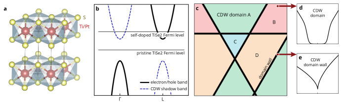
Pure 1T-\ceTiSe_, whose crystal structure is shown in Fig. 1a, undergoes a charge density wave (CDW) transition at 200 K with a charge order [2]. While the nature of this CDW has been a matter of debate for decades, many of the recent experimental studies favor the electronically driven CDW [3, 4, 5, 6, 7, 8, 9, 10], consistent with the theoretical description of excitonic insulator [11, 12]. Nevertheless, a transport study has found finite resistivity in polycrystalline \ceTiSe2 samples at low temperature [13], consistent with metallic behavior. The sensitivity of the low-temperature transport property on the synthesis condition [14] suggests that the observed metallic behavior in the polycrystalline sample is likely due to self-doping (see Fig. 1b).
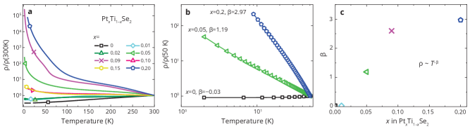
The temperature-dependent resistivity data on single crystals (Fig. 2a) give a high-to-low temperature resistivity ratio with an exponent that is 0 for dopings (metallic behavior), and (up to ) for (insulating behavior), indicative of MIT at around Pt doping with a remarkable orders of magnitude increase in the scaled resistivity compared to the compound. [ is an average nominal composition, which can vary locally within a crystal.] Around this composition, the signatures of the CDW transition are also obscured by the diverging resistivity, consistent with the observation on the polycrystalline samples. The temperature dependence of the resistivity in the insulating phase does not fit either the activated form or variable range hopping, . This is more clearly seen in the Zabrodskii plot [15] (Supplementary Note 1, Supplementary Fig. 1) where the zero slope suggests that the temperature dependence follows a power-law behavior, without any exponential factor, as seen in Fig. 2b and the doping dependence in Fig. 2c.
The high sensitivity of resistivity to Pt substitution as well as the unusual temperature-dependent resistivity point toward a highly unusual insulating state. In this paper, we use a combination of electrical transport, angle-resolved photoemission spectroscopy (ARPES), and scanning tunneling microscopy (STM) to determine the mechanism for MIT in these compounds. Guided by the STM and ARPES data, we propose a model of narrow metallic channels on the domain walls of CDW, in an otherwise insulating background (See. Fig. 1), which potentially provides explanations for the power-law temperature dependence of the resistivity, and points to an alternative path to obtain an MIT.
RESULTS AND DISCUSSION
Effects of Pt dopants
We find that Pt in 1T-\ceTiSe_ has two effects: (1) Our Hall measurements suggest that the Pt dopants introduce electron-like carriers to the system (see Supplementary Fig. 2). Usually, such carrier doping of a semimetal/semiconductor drives the system towards a metallic phase; this, however, is the opposite of what we find in 1T-\cePt_Ti_Se_. (2) Our DFT calculations find that it is energetically favorable for a Pt to substitute Ti rather than to intercalate. (See Supplementary Note 3.) Its orbitals have higher energy than the orbitals of Ti, thus acting as a local potential impurity. This Pt substitution is further corroborated by the shapes of the defects observed in topography images from scanning tunneling microscopy (shown in Supplementary Fig. 7) and reaffirms the experimental finding on polycrystalline samples [13].
Pseudogap-like behavior observed in angle-resolved photoemission spectroscopy
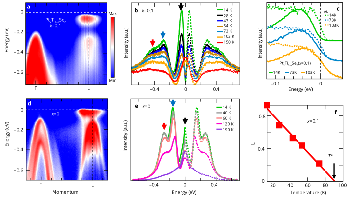
To gain insight into the MIT in 1T-\cePt_Ti_Se_, we study the evolution of the single-particle spectral function of the doped single crystals from the metallic to the insulating regime using ARPES. Figures 3a and d show the energy-momentum intensity maps (EMIMs) [16] around the L point for and , respectively. The EMIM depicts the ARPES intensity as a function of one of the in-plane momentum components and electronic energy referenced to the chemical potential , while keeping the other orthogonal in-plane momentum component fixed. Both samples show a hole-like band near the point and its CDW shadow near the L point. Compared to that of the sample, the shadow band of the sample is much weaker and broader, indicating the loss of long-range CDW correlation with doping. Interestingly, the sample shows suppression of the spectral weight at the Fermi level near the L point, which we discuss next.
The contrast between doped and undoped samples can be seen by examining the energy distribution curves (EDCs) in Figs. 3b and e, which show ARPES data as functions of at a specific momentum. To detect energy gaps near , it is necessary to eliminate the effect of the Fermi function from the EDCs. This can be approximately taken into account by employing symmetrization technique [17, 18]. A different method to accomplish this is to divide the EDCs by resolution-broadened Fermi function [17, 18]. In order to compare results obtained from these two different techniques, we have conducted Fermi function division analysis of the EDCs from sample at various temperatures, which are presented in Supplementary Fig. 6. These are similar to the data in Fig. 3b. For , the symmetrized EDCs (Fig. 3e) exhibit a peak at at all measured temperatures implying the absence of any energy gap. The data for the sample, (Fig. 3b) is markedly different. At higher temperatures of 103 K, the data show peaks at , indicating the absence of an energy gap. With decreasing temperature, however, the peaks of the symmetrized EDCs appear away from , implying gapped electronic excitations. It is to be noted that this energy gap is soft, meaning that there is finite spectral weight at even at the lowest measured temperatures. This prompts us to refer to this energy gap as a pseudogap. We note that this pseudogap can be independently verified from the STM data as well (Fig. 4h), as we will show later.
The temperature evolution of the energy gap can also be investigated via leading-edge analysis of the ARPES data. To this end, we focus on Fig. 3c, where we compare the leading edges of the sample and a polycrystalline gold sample at several temperatures (14 K, 73 K, and 103 K). Comparisons at several other temperatures (28 K, 43 K, 54 K, and 150 K) have been displayed in Supplementary Fig. 5 of Supplementary Note 4. Collectively, these figures show that the leading edge of the EDCs of the Pt-doped sample () is shifted towards negative energy with respect to that of gold at each measured temperature below 103 K indicating the presence of an energy gap. This shift disappears for 103 K, which evidences the absence of an energy gap.
Interestingly, ARPES data suggest that the pseudogap does not “close,” rather it gets “filled-up.” This can be seen by tracking the peak positions of the symmetrized EDCs as a function of temperature. For we find that that the energy location of the peak of each symmetrized EDC is practically the same. There is, however, a monotonic increase in the spectral weight at with increasing temperature from 14 onward. Based on this, we speculate that it is the gradual increase in spectral weight at with increasing temperature that plays a dominant role in the eventual disappearance of the pseudogap at higher temperatures. These observations are reminiscent of the temperature dependence of the pseudogap in underdoped cuprate high-temperature superconductors [19, 20]. We, however, do not suggest that the pseudogap has the same origin in these two very different systems.
We can obtain an estimate for associated with the filling up of the pseudogap. To do this, we define a parameter , where is the intensity of the symmetrized EDC at , and is the energy at the peak of the symmetrized EDC. is the intensity at . is then determined by the temperature at which vanishes [21, 22]. From Fig. 3f, is estimated to be , which is consistent with the observation of peaks at in the symmetrized EDCs for in Fig. 3b as well as with the leading edge comparison with Au shown in Fig. 3c.
ARPES data, therefore, reveal crucial information on the opening of a pseudogap at the chemical potential, which provides potential clues to the dramatic increase in resistivity with Pt-substitution, but also leaves us with some unanswered questions on the origin of the gap. Since the chemical potential shifts up into the conduction band with doping, a transition to a band insulator cannot be the origin of the gap. CDW is also unlikely to be the cause since the ordering is stronger in the undoped sample which is gapless at the chemical potential. In addition, we do not see evidence of hybridization of the conduction band with another band separated by the CDW wavevector. On the other hand, the fact that the gap fills up with increasing temperature suggests that it is a correlation-driven gap, which raises the question of why correlation effects in Pt-substituted \ceTiSe2 are so different from the parent \ceTiSe2.
Domain wall network revealed by scanning tunneling microscopy
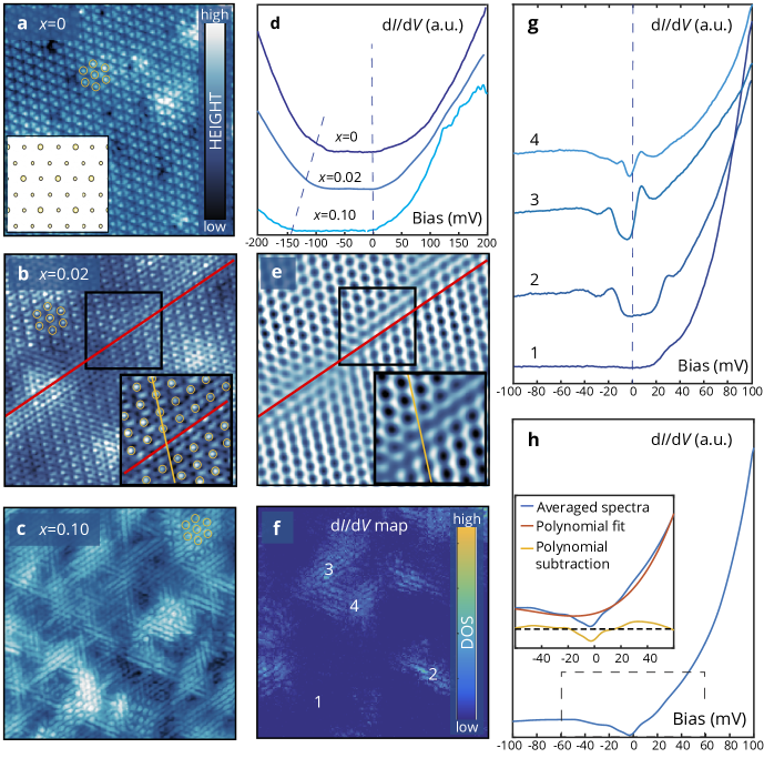
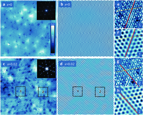
To determine the origin of the pseudogap in 1T-\cePt_Ti_Se_, we turn to local properties using STM. 1T-\cePt_Ti_Se_ single crystals were cleaved at 80 before being inserted into the STM head held at 4 K. From STM topography shown in Figs. 4a-c (also see Supplementary Note 5, Supplementary Figs. 7–9), we find that the sample becomes increasingly disordered with the Pt doping, although the CDW survives as a short-range ordered state (Supplementary Fig. 9). Through selective inverse Fourier transform (explained in Supplementary Note 6), we can identify that the origin of the disorder is due to the increase in the domain wall density (see Fig. 5). This is consistent with the ARPES observation that the back-folded band becomes broader and weaker with Pt-doping.
The overall trend of the STM spectra with Pt doping can be seen in the typical STM spectra obtained far from impurities or domain walls for , , and samples as shown in Fig. 4d. The U shape of the spectra is consistent with the band gap of a semiconductor with a flat bottom representing the bulk indirect band gap between the p- and d- states. Intrinsic doping leads to the Fermi energy being positioned close to the bottom of the conduction band for each of these values. A closer look at the density of states (Supplementary Fig. 11) indicates that for these pristine samples, the Fermi energy lies slightly inside the conduction band, resulting in metallic transport behavior. STM data show that the gap between the conduction and valence bands increases with increasing (dotted lines in Fig. 4d) which is consistent with ARPES data in Figs. 3a and d.
We now focus on the behavior of the local density of states (LDOS) in the samples. An interesting picture emerges from our study of maps (measured at in the same area as the topography in Fig. 4c) that reveals regions with different density-of-states behaviors. In the larger area region within the domains denoted as 1 in Figs. 4f and g the density of states is close to zero around with the conduction band bottom seemingly shifted to higher energies. On the other hand, in the regions denoted by 2, 3, and 4, spatially correlated with the location of the domain walls as identified by the topography, we observe a finite density of states around with a small pseudogap. This suggests that there is a charge or spectral weight transfer from the domains to the domain walls.
The spatially averaged spectrum shown in Fig. 4h shows pseudogap, i.e., a depletion in the density of states relative to background on an energy scale of 30 meV around , which is highlighted when a polynomial background is subtracted (see inset to Fig. 4h as well as Supplementary Fig. 10). Of importance is our observation that the energy scale of the pseudogap is comparable to the one observed by ARPES. Similar pseudogap features are not visible in the averaged spectra of the samples (Supplementary Fig. 10). Based on this we can conclude that the pseudogap feature for sample can be independently observed from STM and the associated energy scales qualitatively agree with the ARPES observations. In addition, STM provides a detailed local view that the Pt dopants disrupt the CDW and affects the local electronic spectra (see also Supplementary Note 5, Supplementary Figs. 7–9). It is thus important to understand the role of the Pt dopants theoretically.
It is encouraging that the pseudogap measured in ARPES agrees with the pseudogap in the averaged density of states; it is, however, unclear how with a finite density of states at zero energy, the resistivity in the Pt-substituted samples could be 5 orders of magnitude larger than the as-grown samples.
Emergent network of narrow transport channels
The substituted Pt acting simply as scattering centers for the charge carriers does not explain the extreme sensitivity of transport property to doping. The Pt dopants, however, can provide a pinning potential for the commensurate CDW. Following the argument by Imry and Ma [23], two dimensions is the lower critical dimension for commensurate order with a random field. This suggests that in \ceTiSe2, which is a layered system with weak interlayer coupling, Pt dopants can strongly disrupt the long-ranged CDW order. This is consistent with the large heterogeneity in the LDOS measured by STS in the doped samples (Figs. 4c, f, and g), and also provide a possible explanation for the dramatic impact of doping on transport.
The large resistance increase and the transition to an insulating phase suggest a model in which the introduction of Pt in \ceTiSe2 produces an irregular network of channels as shown by the STM images. Our DFT calculations indicate a large potential difference between Ti and a Pt impurity that substitutes for Ti. The effect of such an impurity on a CDW material is akin to a stone impacting a glass surface and producing cracks. While the understanding of the precise mechanism for the creation of domain walls is left for a future study, our results paint a picture of the consequences of having domain walls after Pt substitution. The STM LDOS indicates that the charge within the self-doped \ceTiSe2 moves into the domain walls creating a large full gap inside domains and a weaker pseudogap within the domain wall. Thus dc transport occurs primarily via the network of domain walls with the resistance being dominated at the interconnects.
The power-law has previously been observed in (quasi-) one-dimensional systems [24, 25, 26, 27, 28, 29, 30, 31, 32, 33, 34, 35, 36, 37, 38, 39] and was interpreted as due to Luttinger liquid physics. In such a scenario, the power-law suppression of the LDOS should be due to the tunneling of an electron into a system in which the elementary particles are not electrons but fractionalized charge and spin bosonic collective modes. In spite of the suppressed LDOS, the resistance of a clean Luttinger channel vanishes at zero temperature [40], except for the contact resistance. This is a singular example of the role of vertex corrections in strongly modifying the transport behavior from that reflected in the single-particle Greens function and LDOS. The observed resistivity in this case then should arise from strong scattering at the interconnects of the network of Luttinger channels created in Pt-substituted \ceTiSe2—a Luttinger liquid junction formed between intersecting channels can lead to a diverging resistance [41].
Networks of metallic domain walls have previously been observed in Cu-intercalated TiSe2 [42], and also in other contexts: integer quantum Hall systems [43], magnetically ordered systems [44], nearly commensurate charge density wave systems [45], and also recently in moiré systems [46, 47, 48, 49] with periodic networks determined by the moiré pattern. Remarkably, power laws have also been observed in the mass transport through a network of dislocations in solid 4He generated by a pressure difference [50], suggesting a more ubiquitous occurrence of the network of narrow channel transport. The mechanism for the generation of networks is system-specific—disorder, quench, dislocation, etc. Nevertheless, the transport properties at temperatures below the domain gap scale are determined by the electronic structure of the network, as well as its connectivity. A recent theoretical work shows that a network of Luttinger channels supports a stable insulating fixed point with power-law temperature dependence [51].
Let us point out that Luttinger liquid network is not the only explanation for the power-law-like temperature dependence. Another possible mechanism for an insulating behavior with power-law temperature dependence is the “rare chain hopping,” [52, 53, 54, 55, 56, 57], which describes the transport behavior of percolating channels whose resistivity is controlled by the connectivity to the network. It leads to a much weaker dependence compared to variable range hopping, which may appear as a power law in a limited temperature range. Nevertheless, the formation of one-dimensional conduction channels is a crucial ingredient in the rare chain hopping model.
In summary, through a collective study of transport, ARPES, and STS, we argue that the low energy insulating behavior in Pt-doped TiSe2 arises as a result of an interplay between electron correlation and disorder, and is governed by an emergent network of CDW domain walls behaving as narrow channels of low energy transport (see Figs. 1c-e).
Going further, it would be interesting to study whether the MIT mechanism discussed here applies to other systems with CDW. Immediate questions specific to TiSe2 are how unique is the effect of Pt, and whether other substitutions act similarly. Our preliminary investigations with other substitutions indicate a much smaller increase of resistivity, by less than an order of magnitude, as opposed to the five orders of magnitude increase with Pt.
More broadly, our finding that the CDW domain walls provide one-dimensional channels of transport has implications for other CDW systems. In the Cu-intercalated \ceTiSe2 where superconductivity and the incommensurate CDW are observed around the same doping [58], the domain walls could play a major role by channeling electrons into these narrow channels and thereby enhance correlation effects for superconductivity and magnetism. As was pointed out in Ref. [59], when the superconductivity coexists with the CDW close to commensurate-incommensurate transition, the network of domain walls can lead to percolative superconductivity.
METHODS
First-principles calculation
The first-principles band structure and the partial density of states (pDOS) of pure \ceTiSe2 and PtSe2 were calculated using the modified Becke-Johnson potential [60, 61] as implemented in the WIEN2k package [62]. Spin-orbit coupling was not included in the calculation throughout this paper. For simplicity, in these calculations, we used the experimental lattice constants Å and Å for TiSe2 [13] and Å and Å for PtSe2 [63] with the fixed internal coordinate where Ti or Pt is placed on the plane.
For the energy comparison between different Pt positions, we optimized the crystal structures using the DFT-D3 energy functional [64] as implemented in the Vienna ab initio simulation package [65, 66, 67, 68, 69]. Calculations for the cases (2) and (3) employed the supercell.
For the calculation of the onsite energies of the Wannier orbitals, we calculated the band structure of PtTi17Se36 using the supercell, and then extracted the Wannier functions of the Pt- Ti- model using the WIEN2k, Wien2Wannier, and Wannier90 softwares [70, 71, 72, 73]. We omitted the maximal localization procedure. The crystal structure was fixed throughout the calculations for simplicity.
Growth
Single crystals of \cePt_Ti_Se2 were grown by chemical vapor transport using excess Se as the transport agent. Stoichiometric amounts of Pt and Ti, as well as Se power with approximately 50% excess Se by mass were sealed in evacuated quartz tubes of approximately 6 inches in length and 0.5 inches in diameter. Samples were heated in a gradient furnace for ten days minimum at a gradient of 900-1100C then cooled to room temperature. Reported doping amounts in this study are for nominal compositions.
ARPES
Temperature-dependent ARPES measurements on undoped and Pt-doped 1T-\ceTiSe_ single crystals were performed using a Scienta R4000 electron analyzer at the SIS beamline of Swiss Light Source, Paul Scherrer Institute, Switzerland. The measurements were performed using plane-polarized light with 45 eV photon energies (). The energy and momentum resolutions were approximately 10–20 meV and 0.0055 , respectively.
STM
The experiment was performed in an ultrahigh vacuum (UHV) system with a base pressure lower than 10-10 mbar and at a temperature of 4 K. The samples were cleaved at room temperature and immediately inserted into the STM scanner at 4 K. Differential conductance () spectra were acquired using a standard lock-in technique.
DATA AVAILABILITY
All relevant data are available from the corresponding author upon reasonable request.
ACKNOWLEDGEMENTS
K.L. and N.T. acknowledge support from National Science Foundation (NSF) Grant No. DMREF-1629382. J.C., C.L.H., and E.M. acknowledge support from NSF Grant No. DMREF-1629374. D.I., Z.W., and V.M. acknowledge support from NSF Grant No. DMREF-1629068. J.L., J.Z., and U.C acknowledge support from NSF Grant No. DMREF-1629237. M.S., J.M., and M.Y. were supported by the Sino-Swiss Science and Technology Cooperation Grant No. IZLCZ2-170075. R.A. acknowledges the financial support of Japan Society for the Promotion of Science Kakenhi Grant No. 16H06345.
COMPETING INTERESTS
The authors declare no competing interests.
AUTHOR CONTRIBUTIONS
K.L. and N.T. performed theoretical modeling. J.C., C.L.H., and E.M. grew the crystals and performed the transport measurements. D.I., Z.W., and V.M. performed the STM measurements. J.L., J.Z., M.S., J.M., M.Y., and U.C. performed the ARPES measurements. M.O. and R.A. performed the DFT calculations.
References
- [1] J. Ishioka et al. “Chiral charge-density waves” In Phys. Rev. Lett. 105 American Physical Society, 2010, pp. 176401 DOI: 10.1103/PhysRevLett.105.176401
- [2] F.. Di Salvo, D.. Moncton and J.. Waszczak “Electronic properties and superlattice formation in the semimetal TiSe2” In Phys. Rev. B 14.10, 1976, pp. 4321–4328 DOI: 10.1103/PhysRevB.14.4321
- [3] M.. Traum et al. “: Semiconductor, semimetal, or excitonic insulator” In Phys. Rev. B 17 American Physical Society, 1978, pp. 1836–1838 DOI: 10.1103/PhysRevB.17.1836
- [4] H. Cercellier et al. “Evidence for an excitonic insulator phase in -” In Phys. Rev. Lett. 99 American Physical Society, 2007, pp. 146403 DOI: 10.1103/PhysRevLett.99.146403
- [5] Katsuaki Sugawara et al. “Unconventional charge-density-wave transition in monolayer -TiSe2” In ACS Nano 10.1 American Chemical Society, 2016, pp. 1341–1345 DOI: 10.1021/acsnano.5b06727
- [6] B. Hildebrand et al. “Short-range phase coherence and origin of the - charge density wave” In Phys. Rev. B 93 American Physical Society, 2016, pp. 125140 DOI: 10.1103/PhysRevB.93.125140
- [7] C. Monney et al. “Revealing the role of electrons and phonons in the ultrafast recovery of charge density wave correlations in -” In Phys. Rev. B 94 American Physical Society, 2016, pp. 165165 DOI: 10.1103/PhysRevB.94.165165
- [8] Anshul Kogar et al. “Signatures of exciton condensation in a transition metal dichalcogenide” In Science 358.6368 American Association for the Advancement of Science, 2017, pp. 1314–1317 DOI: 10.1126/science.aam6432
- [9] H. Hedayat et al. “Excitonic and lattice contributions to the charge density wave in - revealed by a phonon bottleneck” In Phys. Rev. Research 1 American Physical Society, 2019, pp. 023029 DOI: 10.1103/PhysRevResearch.1.023029
- [10] M.-L. Mottas et al. “Semimetal-to-semiconductor transition and charge-density-wave suppression in - single crystals” In Phys. Rev. B 99 American Physical Society, 2019, pp. 155103 DOI: 10.1103/PhysRevB.99.155103
- [11] C. Monney et al. “Exciton condensation driving the periodic lattice distortion of -” In Phys. Rev. Lett. 106 American Physical Society, 2011, pp. 106404 DOI: 10.1103/PhysRevLett.106.106404
- [12] Chuan Chen, Bahadur Singh, Hsin Lin and Vitor M. Pereira “Reproduction of the charge density wave phase diagram in - exposes its excitonic character” In Phys. Rev. Lett. 121 American Physical Society, 2018, pp. 226602 DOI: 10.1103/PhysRevLett.121.226602
- [13] Justin S. Chen et al. “Chemical tuning of electrical transport in Ti1-xPtxSe2-y” In Phys. Rev. B 91 American Physical Society, 2015, pp. 045125 DOI: 10.1103/PhysRevB.91.045125
- [14] Jaime M. Moya et al. “Effect of synthesis conditions on the electrical resistivity of ” In Phys. Rev. Materials 3 American Physical Society, 2019, pp. 084005 DOI: 10.1103/PhysRevMaterials.3.084005
- [15] A.. Zabrodskii and K.. Zinov’eva “Low-temperature conductivity and metal-insulator transition in compensate n-Ge” In Zh. Eksp. Teor. Fiz. 86.2, 1984, pp. 727–742
- [16] J. Zhao et al. “Spectroscopic fingerprints of many-body renormalization in ” In Phys. Rev. B 100 American Physical Society, 2019, pp. 045106 DOI: 10.1103/PhysRevB.100.045106
- [17] J.. Campuzano, M.. Norman and M. Randeria “Photoemission in the High- Superconductors” In Physics of Superconductors II Berlin: Springer, 2004, pp. 167–273
- [18] Andrea Damascelli, Zahid Hussain and Zhi-Xun Shen “Angle-resolved photoemission studies of the cuprate superconductors” In Rev. Mod. Phys. 75 American Physical Society, 2003, pp. 473–541 DOI: 10.1103/RevModPhys.75.473
- [19] M.. Norman et al. “Destruction of the Fermi surface in underdoped high- superconductors” In Nature 392.6672, 1998, pp. 157–160 DOI: 10.1038/32366
- [20] U. Chatterjee et al. “Emergence of coherence in the charge-density wave state of NbSe2” In Nat. Commun. 6, 2015, pp. 6313 DOI: 10.1038/ncomms7313
- [21] Yuwen Hu et al. “Charge density waves and phonon-electron coupling in ” In Phys. Rev. B 91 American Physical Society, 2015, pp. 144502 DOI: 10.1103/PhysRevB.91.144502
- [22] Jaydeep Joshi et al. “Short-range charge density wave order in -” In Phys. Rev. B 99 American Physical Society, 2019, pp. 245144 DOI: 10.1103/PhysRevB.99.245144
- [23] Yoseph Imry and Shang-keng Ma “Random-field instability of the ordered state of continuous symmetry” In Phys. Rev. Lett. 35 American Physical Society, 1975, pp. 1399–1401 DOI: 10.1103/PhysRevLett.35.1399
- [24] Marc Bockrath et al. “Luttinger-liquid behaviour in carbon nanotubes” In Nature 397.6720, 1999, pp. 598–601 DOI: 10.1038/17569
- [25] Zhen Yao, Henk W.. Postma, Leon Balents and Cees Dekker “Carbon nanotube intramolecular junctions” In Nature 402.6759, 1999, pp. 273–276 DOI: 10.1038/46241
- [26] A. Bachtold et al. “Suppression of tunneling into multiwall carbon nanotubes” In Phys. Rev. Lett. 87 American Physical Society, 2001, pp. 166801 DOI: 10.1103/PhysRevLett.87.166801
- [27] Akinobu Kanda, Kazuhito Tsukagoshi, Yoshinobu Aoyagi and Youiti Ootuka “Gate-Voltage dependence of zero-bias anomalies in multiwall carbon nanotubes” In Phys. Rev. Lett. 92 American Physical Society, 2004, pp. 036801 DOI: 10.1103/PhysRevLett.92.036801
- [28] B. Gao et al. “Evidence for Luttinger-liquid behavior in crossed metallic single-wall nanotubes” In Phys. Rev. Lett. 92 American Physical Society, 2004, pp. 216804 DOI: 10.1103/PhysRevLett.92.216804
- [29] M. Monteverde et al. “Tomonaga-Luttinger liquid and coulomb blockade in multiwall carbon nanotubes under pressure” In Phys. Rev. Lett. 97 American Physical Society, 2006, pp. 176401 DOI: 10.1103/PhysRevLett.97.176401
- [30] J.. Coiffic et al. “Conduction regime in innovative carbon nanotube via interconnect architectures” In Appl. Phys. Lett. 91.25, 2007, pp. 252107 DOI: 10.1063/1.2826274
- [31] J.-F. Dayen et al. “Conductance of disordered semiconducting nanowires and carbon nanotubes: a chain of quantum dots” In Eur. Phys. J. Appl. Phys. 48.1, 2009, pp. 10604 DOI: 10.1051/epjap/2009132
- [32] S.. Zaitsev-Zotov, Yu.. Kumzerov, Yu.. Firsov and P. Monceau “Luttinger-liquid-like transport in long InSb nanowires” In J. Phys. Condens. Matter 12.20 IOP Publishing, 2000, pp. L303–L309 DOI: 10.1088/0953-8984/12/20/101
- [33] A.. Chang “Chiral Luttinger liquids at the fractional quantum Hall edge” In Rev. Mod. Phys. 75 American Physical Society, 2003, pp. 1449–1505 DOI: 10.1103/RevModPhys.75.1449
- [34] Yaroslav Tserkovnyak, Bertrand I. Halperin, Ophir M. Auslaender and Amir Yacoby “Interference and zero-bias anomaly in tunneling between Luttinger-liquid wires” In Phys. Rev. B 68 American Physical Society, 2003, pp. 125312 DOI: 10.1103/PhysRevB.68.125312
- [35] E. Slot, M.. Holst, H… Zant and S.. Zaitsev-Zotov “One-dimensional conduction in charge-density-wave nanowires” In Phys. Rev. Lett. 93 American Physical Society, 2004, pp. 176602 DOI: 10.1103/PhysRevLett.93.176602
- [36] A.. Aleshin, H.. Lee, Y.. Park and K. Akagi “One-dimensional transport in polymer nanofibers” In Phys. Rev. Lett. 93 American Physical Society, 2004, pp. 196601 DOI: 10.1103/PhysRevLett.93.196601
- [37] Atikur Rahman and Milan K Sanyal “Bias dependent crossover from variable range hopping to power law characteristics in the resistivity of polymer nanowires” In J. Phys. Condens. Matter 22.17 IOP Publishing, 2010, pp. 175301 DOI: 10.1088/0953-8984/22/17/175301
- [38] Latha Venkataraman, Yeon Suk Hong and Philip Kim “Electron transport in a multichannel one-dimensional conductor: molybdenum selenide nanowires” In Phys. Rev. Lett. 96 American Physical Society, 2006, pp. 076601 DOI: 10.1103/PhysRevLett.96.076601
- [39] Zhixian Zhou et al. “One-dimensional electron transport in Cu-tetracyanoquinodimethane organic nanowires” In Appl. Phys. Lett. 90.19, 2007, pp. 193115 DOI: 10.1063/1.2738380
- [40] C.. Kane and Matthew P.. Fisher “Transmission through barriers and resonant tunneling in an interacting one-dimensional electron gas” In Phys. Rev. B 46 American Physical Society, 1992, pp. 15233 DOI: 10.1103/PhysRevB.46.15233
- [41] D.. Aristov, I.. Gornyi, D.. Polyakov and P. Wölfle “Y junction of Luttinger liquid wires out of equilibrium” In Phys. Rev. B 95 American Physical Society, 2017, pp. 155447 DOI: 10.1103/PhysRevB.95.155447
- [42] Shichao Yan et al. “Influence of domain walls in the incommensurate charge density wave state of Cu intercalated -TiSe2” In Phys. Rev. Lett. 118 American Physical Society, 2017, pp. 106405 DOI: 10.1103/PhysRevLett.118.106405
- [43] J.. Chalker and P.. Coddington “Percolation, quantum tunnelling and the integer Hall effect” In J. Phys. C: Solid State Phys. 21.14 IOP Publishing, 1988, pp. 2665–2679 DOI: 10.1088/0022-3719/21/14/008
- [44] Eric Yue Ma et al. “Mobile metallic domain walls in an all-in-all-out magnetic insulator” In Science 350.6260 American Association for the Advancement of Science, 2015, pp. 538–541 DOI: 10.1126/science.aac8289
- [45] Jae Whan Park, Gil Young Cho, Jinwon Lee and Han Woong Yeom “Emergent honeycomb network of topological excitations in correlated charge density wave” In Nat. Commun. 10.1, 2019, pp. 4038 DOI: 10.1038/s41467-019-11981-5
- [46] Shengqiang Huang et al. “Topologically protected helical states in minimally twisted bilayer graphene” In Phys. Rev. Lett. 121 American Physical Society, 2018, pp. 037702 DOI: 10.1103/PhysRevLett.121.037702
- [47] Dmitry K. Efimkin and Allan H. MacDonald “Helical network model for twisted bilayer graphene” In Phys. Rev. B 98 American Physical Society, 2018, pp. 035404 DOI: 10.1103/PhysRevB.98.035404
- [48] S.. Sunku et al. “Photonic crystals for nano-light in moiré graphene superlattices” In Science 362.6419 American Association for the Advancement of Science, 2018, pp. 1153–1156 DOI: 10.1126/science.aau5144
- [49] S.. Xu et al. “Giant oscillations in a triangular network of one-dimensional states in marginally twisted graphene” In Nat. Commun. 10.1, 2019, pp. 4008 DOI: 10.1038/s41467-019-11971-7
- [50] Jaeho Shin and Moses H.. Chan “Mass transport through dislocation network in solid ” In Phys. Rev. B 99 American Physical Society, 2019, pp. 140502 DOI: 10.1103/PhysRevB.99.140502
- [51] Jongjun M. Lee, Masaki Oshikawa and Gil Young Cho Non-Fermi liquids in conducting 2D networks. Preprint at https://arxiv.org/abs/2009.02336, 2020
- [52] M. Pollak and J.. Hauser “Note on the anisotropy of the conductivity in thin amorphous films” In Phys. Rev. Lett. 31 American Physical Society, 1973, pp. 1304–1307 DOI: 10.1103/PhysRevLett.31.1304
- [53] A.. Tartakovskii, M.. M.. Raikh and I.. Ruzin “Hopping conductivity of metal-semiconductor metal contacts” In Sov. Phys. Semicond. 21, 1987, pp. 370–373
- [54] L.. Glazman and K.. Matveev “Inelastic tunneling across thin amorphous films” In Sov. Phys. JETP 67, 1988, pp. 1276–1282
- [55] E.. Levin, I.. Ruzin and B.. Shklovskii “Transverse hopping conductivity of amorphous films in strong electric fields” In Sov. Phys. Semicond. 22, 1988, pp. 401–408
- [56] A.. Rodin and M.. Fogler “Apparent power-law behavior of conductance in disordered quasi-one-dimensional systems” In Phys. Rev. Lett. 105 American Physical Society, 2010, pp. 106801 DOI: 10.1103/PhysRevLett.105.106801
- [57] A.. Rodin and M.. Fogler “Hopping transport in systems of finite thickness or length” In Phys. Rev. B 84 American Physical Society, 2011, pp. 125447 DOI: 10.1103/PhysRevB.84.125447
- [58] E. Morosan et al. “Superconductivity in CuxTiSe2” In Nat. Phys. 2.8, 2006, pp. 544–550 DOI: 10.1038/nphys360
- [59] Chuan Chen, Lei Su, A.. Castro Neto and Vitor M. Pereira “Discommensuration-driven superconductivity in the charge density wave phases of transition-metal dichalcogenides” In Phys. Rev. B 99 American Physical Society, 2019, pp. 121108 DOI: 10.1103/PhysRevB.99.121108
- [60] A.. Becke and E.. Johnson “A simple effective potential for exchange” In J. Chem. Phys. 124.22, 2006, pp. 221101 DOI: 10.1063/1.2213970
- [61] F. Tran and P. Blaha “Accurate band gaps of semiconductors and insulators with a semilocal exchange-correlation potential” In Phys. Rev. Lett. 102 American Physical Society, 2009, pp. 226401 DOI: 10.1103/PhysRevLett.102.226401
- [62] P. Blaha et al. “WIEN2k, An Augmented Plane Wave + Local Orbitals Program for Calculating Crystal Properties” Karlheinz Schwarz, Techn. Universität Wien, Austria, 2001
- [63] S. Furuseth, K. Selte and A. Kjekshus “Redetermined crystal structures of NiTe2, PdTe2, PtS2, PtSe2, and PtTe2” In Acta. Chem. Scand. 19, 1965, pp. 257–258 DOI: 10.3891/acta.chem.scand.19-0257
- [64] Stefan Grimme, Jens Antony, Stephan Ehrlich and Helge Krieg “A consistent and accurate ab initio parametrization of density functional dispersion correction (DFT-D) for the 94 elements H-Pu” In J. Chem. Phys. 132.15, 2010, pp. 154104 DOI: 10.1063/1.3382344
- [65] G. Kresse and D. Joubert “From ultrasoft pseudopotentials to the projector augmented-wave method” In Phys. Rev. B 59 American Physical Society, 1999, pp. 1758–1775 DOI: 10.1103/PhysRevB.59.1758
- [66] G. Kresse and J. Hafner “Ab initio molecular dynamics for liquid metals” In Phys. Rev. B 47 American Physical Society, 1993, pp. 558–561 DOI: 10.1103/PhysRevB.47.558
- [67] G. Kresse and J. Hafner “Ab initio molecular-dynamics simulation of the liquid-metal–amorphous-semiconductor transition in germanium” In Phys. Rev. B 49 American Physical Society, 1994, pp. 14251–14269 DOI: 10.1103/PhysRevB.49.14251
- [68] G. Kresse and J. Furthmüller “Efficiency of ab-initio total energy calculations for metals and semiconductors using a plane-wave basis set” In Comput. Mater. Sci. 6, 1996, pp. 15–50 DOI: https://doi.org/10.1016/0927-0256(96)00008-0
- [69] G. Kresse and J. Furthmüller “Efficient iterative schemes for ab initio total-energy calculations using a plane-wave basis set” In Phys. Rev. B 54 American Physical Society, 1996, pp. 11169–11186 DOI: 10.1103/PhysRevB.54.11169
- [70] Nicola Marzari and David Vanderbilt “Maximally localized generalized Wannier functions for composite energy bands” In Phys. Rev. B 56 American Physical Society, 1997, pp. 12847–12865 DOI: 10.1103/PhysRevB.56.12847
- [71] Ivo Souza, Nicola Marzari and David Vanderbilt “Maximally localized Wannier functions for entangled energy bands” In Phys. Rev. B 65 American Physical Society, 2001, pp. 035109 DOI: 10.1103/PhysRevB.65.035109
- [72] Jan Kunes̆ et al. “Wien2wannier: From linearized augmented plane waves to maximally localized Wannier functions” In Comp. Phys. Commun. 181.11, 2010, pp. 1888–1895 DOI: 10.1016/j.cpc.2010.08.005
- [73] Arash A. Mostofi et al. “wannier90: A tool for obtaining maximally-localised Wannier functions” In Comp. Phys. Commun. 178.9, 2008, pp. 685–699 DOI: 10.1016/j.cpc.2007.11.016