Incorporation of erbium ions into thin-film lithium niobate integrated photonics
Abstract
As an active material with favorable linear and nonlinear optical properties, thin-film lithium niobate has demonstrated its potential in integrated photonics. Integration with rare-earth ions, which are promising candidates for quantum memories and transducers, will enrich the system with new applications in quantum information processing. Here, we investigate the optical properties at 1.5 micron wavelengths of rare-earth ions (Er3+) implanted in thin-film lithium niobate waveguides and micro-ring resonators. Optical quality factors near a million after post annealing show that ion implantation damage can be successfully repaired. The transition linewidth and fluorescence lifetime of erbium ions are characterized, revealing values comparable to bulk-doped crystals. The ion-cavity coupling is observed through a Purcell enhanced fluorescence, from which a Purcell factor of 3.8 is extracted. This platform is compatible with top-down lithography processes and leads to a scalable path for controlling spin-photon interfaces in photonic circuits.
As an important material in modern photonics, lithium niobate (LN) displays favorable piezoelectric, electro-optic, optical, photoelastic and photorefractive properties [1]. It is widely used for electro-optic modulators, frequency doublers, optical parametric oscillators and Q-switches for lasers. However, LN had been limited to bulk crystal components in all of these applications until a recent breakthrough in LN thin-film nanofabrication technology [2] made compact and dense photonic integrated circuits possible. Subsequent works on high-performance electro-optical modulators [3, 4], ultra-efficient second harmonic generation [5, 6] and microwave-optical transduction [7] have stimulated intense interest and promise for integrated photonics. This advance in LN thin-film nanofabrication technology also raises the interest in incorporating rare-earth ions (REIs) into patterned LN waveguides and micro-cavities for scalable photonic integrated circuits with added functionalities enabled by the REIs.
REIs are well known for their applications in nonlinear optics such as lasers and amplifiers[8] due to their stable optical transitions, high fluorescence quantum efficiencies, and long population lifetimes. Their narrow homogeneous linewidths[9, 10], which allow the burning of ultra-narrow spectral holes, also find themselves useful in photonic signal processing[11] as well as frequency stabilization [8, 12, 13], medical imaging[14] and optical filtering[8, 15]. Over the past decades, REIs have emerged as a promising candidate for quantum information processing[16, 17, 18] thanks to the weak coupling of their 4f electrons to the environment[19] and long coherent spin states [20]. REIs have been used to demonstrate quantum memory protocols for quantum networks [21], light-matter interactions[22] and quantum-state teleportation[23]. Among the several well-studied REIs, erbium (Er) has received much attention due to its optical transitions in the telecommunications band, avoiding the need for frequency conversion and reducing the complexity of the system. There are already past efforts in incorporating erbium ions into various hosts for integrated photonics such as bulk LN[24], yttrium orthosilicate (YSO) crystals[25], and silicon nitride[26]. However, there is still a knowledge gap in combining erbium ions with LN thin-film structures, which could open a vital avenue to harness the benefit of both systems.
In this Letter, we investigate the Er doping of LN photonic devices through ion implantation. We observe recovery of the optical performance of the LN thin-film nanostructures after post-annealing that repairs the lattice damage caused by implantation. The transition linewidth and fluorescence lifetime of the implanted ions inside optical waveguides are then characterized. The enhanced interaction of erbium ions with micro-cavities, which can be utilized to overcome the small oscillator strength of REIs, is demonstrated through the Purcell effect.
Commercial (NanoLN) thin-film wafers of 600 nm-thick z-cut lithium niobate on insulator (LNOI) are chosen for device fabrication and subsequent ion implantation. We fabricate micro-ring resonators and centimeter-long waveguides by patterning hydrogen silsesquioxane (HSQ) on LN thin film with electron beam lithography (EBL). Ring radius is designed to be 70 m. The ring and the waveguide widths are 1.8 m and 800 nm respectively. The coupling gap between the ring and the bus waveguide is varied from 400 nm to 1000 nm to identify the critical coupling condition. Grating couplers optimized for the transverse electric (TE) mode at 1532 nm are used to efficiently screen many devices. The structures are then half-etched through reactive ion etching (RIE) with argon plasma. Fig. 1a)i shows the scanning electron microscope (SEM) image of a grating coupler and Fig. 1a)ii shows the SEM image of the coupling region of a ring resonator. Fig. 1a)iii shows a schematic of the cross section of a ring resonator with a 60 degree etched side wall. The TE fundamental mode is well confined inside the half-etched ring. The ring resonators exhibit an average Q of 500 k after post fabrication annealing at 500 °C for 5 hours.
Before erbium implantation, 30 nm-thick SiO2 is deposited on the chip by plasma-enhanced chemical vapor deposition (PECVD). The erbium ions are doped with an implantation energy of 350 keV and a flux fluence of 1.141014 ions/cm2. The stopping and range of ions in matter (SRIM)[27] simulation (Fig. 1a)iv) estimates that the peak ion density is around 80 nm deep from the top surface with the tail of the distribution extending to the SiO2/LiNbO3 interface. This corresponds to an average implantation depth of 50 nm into the LN thin film.
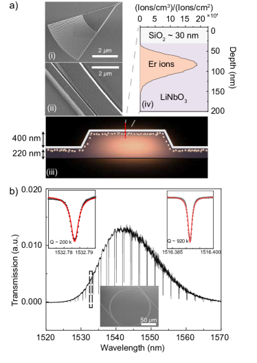
Post-implantation annealing is carried out at various temperatures to repair the lattice damage from implantation. A temperature of 350 °C is sufficient to recover the transmission, but the maximum Q is not achieved until 550 °C. A typical grating coupler transmission measurement is shown in Fig. 1b), in which fundamental and first-order TE modes of the resonator can be observed. The bottom inset of Fig. 1b) shows a typical ring resonator with bus waveguides. A resonance with a Q of around 200 k at around 1532 nm in the device used for later experiments is shown in the inset at the top-left corner. It is worth noting that several high-Q resonances could be found in other ring resonators, one of which had a Q of nearly a million at 1516 nm, as shown in the inset at the top-right corner. The average Q of the devices after post-implantation annealing at 550 °C is 500 k, indicating that a full recovery of optical performance of the nanostructure is possible.
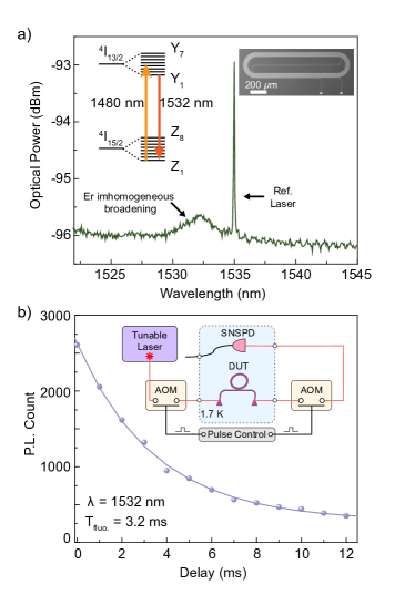
Fig. 2a) shows a room temperature fluorescence measurement to map the inhomogeneous broadening of erbium ions. The experiment is carried out on a 4.7 cm-long waveguide (top-right inset of Fig 2a)). A strong optical pump at 1480 nm is used to excite the Er3+ ions and the spectral response is mapped with a tunable filter. A reference laser is introduced to calibrate the tunable filter.
The crystal structure of LN is described by space group where Li+ and Nb3+ ions sit along the trigonal axis. When the Er3+ ions sit at the Li+ site, their point group is .[28] This crystal field splits the Er3+ ground electronic state () into 8 Kramer doublets labeled as and the Er excited electronic state () into 7 Kramer doublets labeled as . The optical pump at 1480 nm coincides with a strong absorption peak of the transition[29]. Fast non-radiative decay[30] first relaxes the state to and then optically relaxes to the ground Stark state by emiting a photon at 1532 nm. This process is illustrated in the top-left inset of Fig. 2a). The Er3+ fluorescence signal as well as the signature of the reference laser are shown clearly in Fig. 2a). The room temperature Er3+ fluorescence peak is centered at around 1532 nm, and a Lorentz fit yields a linewidth of 250 GHz. This linewidth is comparable to the literature value of 180 GHz for the low-temperature inhomogeneous broadening in bulk-doped crystals [8]. The small increase is likely due to additional homogeneous broadening from phonon scattering at room temperature, although there may also be a contribution from crystal strain[31] caused by bonding the LN thin film to the oxide substrate. The device is then cooled down to 1.7 K, where a resonant excitation measurement is done to extract the population lifetime of the Er3+ ions. The inset of Fig. 2b) shows the experiment schematic. Two accousto-optic modulators (AOM) are placed before and after the device for gating to resonantly pump and measure the fluorescence at 1532 nm using a continuous-wave tunable laser and a fiber-coupled superconducting nanowire single-photon detector (SNSPD)[32]. A single exponential fit of the fluorescence decay allows us to extract a lifetime of 3.2 ms. This is somewhat longer than the excited-state lifetime of 2.0 ms measured for a bulk-doped crystal by spectral hole burning[33]. Fluorescence lifetimes for bulk-doped crystals are usually significantly longer than the excited-state lifetime due to the strong fluorescence absorption and re-emission that occurs for this transition[34], which likely also causes the longer lifetime observed here.
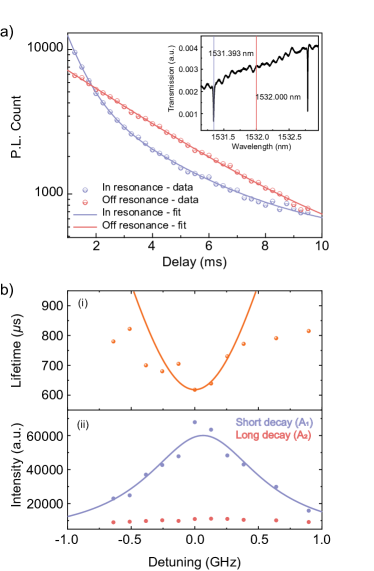
To demonstrate the ion-cavity coupling, we focus on a resonance near 1532 nm in a ring resonator and extract the Purcell-enhanced fluorescence decay rate. The fluorescence decay when pumping on- and off-resonance are compared in Fig. 3a). Due to the interaction with the cavity field, the fluorescence lifetime of an ion in the ring resonator should be shortened compared to the value in the bus waveguides outside of the cavity , according to[35]
| (1) |
where is the decay rate of the ring resonator and is the detuning from the resonance frequency . The coupling rate between the ion and resonator can be written as
| (2) |
where , [36] and are the dipole moment, refractive index and resonator mode volume. The coupling also depends on the position of the ion, which is quantified by the spatial overlap with the cavity mode . By substituting Eq. 2 into Eq. 1, we arrive at the formula for the Purcell factor at zero detuning
| (3) |
To quantify the coupling rate and the Purcell factor, we first fit the fluorescence measurement off-resonance from the cavity with a single exponential decay function
| (4) |
where ms is obtained. For the on-resonance case, however, there are two groups of ions contributing to the fluorescence, e.g. one in the ring resonator, and the other in the bus waveguide. For simplicity, we approximate the influence of the cavity field with a Purcell enhanced lifetime averaged over all of the ions at different locations. Then the overall fluorescence from on-resonance pumping should be fitted with a double exponential decay function, fixing the long time constant at ,
| (5) |
As shown in Fig. 3a), the experimental data are well approximated by this double exponential decay function, giving s. The average Purcell factor is then calculated to be , and the coupling rate kHz.
The measured value of Purcell enhancement can be theoretically modeled by Eq. 3. For the selected resonance at 1531.393 nm, we measure k. From the simulation results of the field distribution, we calculate the mode volume m3, and an average value of field overlap for the simulated implantation depth of 50 nm. This results in an overall Purcell enhancement , which is close to the experimental value of 3.8. We note that further improvement of the Purcell enhancement requires a resonance with a higher , a smaller mode volume and a better spatial overlap . For the current batch of devices, the enhancement could be about 5 times higher if the high-Q resonance was centered around the Er3+ transition wavelength of 1532 nm. Another factor of 8 improvement would also be possible if the Er3+ ions are incorporated into the center of the resonator.
We also examine the fluorescence decay when the pumping frequency is detuned from the resonance. Fig. 3b)i shows the measured lifetime of the ions in the ring resonator, extracted from the double exponential fit, as well as the theoretical curve calculated based on Eq. 1. The corresponding fluorescence intensities from the ring and the bus waveguide portions are plotted in Fig. 3b)ii. It is clear that the fluorescence from the waveguide () is insensitive to the detuning from the resonance, while the fluorescence from the ring resonator () peaks at zero detuning. Likewise, we theoretically model the enhanced fluorescence signal from the ions in the ring resonator () by a Lorentzian curve with being a fitting parameter. The model matches the data well in Fig. 3b)ii, showing a clear resonance-enhanced fluorescence decay.
In conclusion, we introduce Er-implanted LN thin-film nanostructures and investigate their optical properties. We show that the cavity properties in the doped device could be recovered by post-implantation annealing with a temperature of up to 550 °C, obtaining resonances with a loaded Q of near a million after annealing. The transition linewidth and population lifetime of the erbium ions are extracted in waveguides and resonant cavities through fluorescence measurements. We show that the optical emission of ions in the ring resonator is cavity-enhanced and that the experimental data match theoretical models well, with an average Purcell enhancement of 3.8. This work demonstrates the possibility to fabricate a compact and scalable platform for spin-photon interfaces with LN-based integrated photonics.
Note added: In preparing this manuscript, the authors noticed that a related pre-print discussing a different rare-earth element (Tm) in bulk-doped LN thin-film waveguides[37].
This work is supported by Department of Energy, Office of Basic Energy Sciences, Division of Materials Sciences and Engineering under Grant DE-SC0019406. The authors would like to thank Dr. Yong Sun, Sean Rinehart, Kelly Woods, and Dr. Michael Rooks for their assistance provided in the device fabrication. The fabrication of the devices was done at the Yale School of Engineering & Applied Science (SEAS) Cleanroom and the Yale Institute for Nanoscience and Quantum Engineering (YINQE).
REFERENCES
References
- Weis and Gaylord [1985] R. S. Weis and T. K. Gaylord, “Lithium niobate: summary of physical properties and crystal structure,” Applied Physics A 37, 191–203 (1985).
- Zhang et al. [2017] M. Zhang, C. Wang, R. Cheng, A. Shams-Ansari, and M. Lončar, “Monolithic ultra-high-q lithium niobate microring resonator,” Optica 4, 1536–1537 (2017).
- Wang et al. [2018] C. Wang, M. Zhang, X. Chen, M. Bertrand, A. Shams-Ansari, S. Chandrasekhar, P. Winzer, and M. Lončar, “Integrated lithium niobate electro-optic modulators operating at cmos-compatible voltages,” Nature 562, 101 (2018).
- He et al. [2019] M. He, M. Xu, Y. Ren, J. Jian, Z. Ruan, Y. Xu, S. Gao, S. Sun, X. Wen, L. Zhou, et al., “High-performance hybrid silicon and lithium niobate mach–zehnder modulators for 100 gbit s- 1 and beyond,” Nature Photonics 13, 359 (2019).
- Lu et al. [2019] J. Lu, J. B. Surya, X. Liu, A. W. Bruch, Z. Gong, Y. Xu, and H. X. Tang, “Periodically poled thin-film lithium niobate microring resonators with a second-harmonic generation efficiency of 250,000%/w,” Optica 6, 1455–1460 (2019).
- Chen et al. [2019] J.-Y. Chen, Z.-H. Ma, Y. M. Sua, Z. Li, C. Tang, and Y.-P. Huang, “Ultra-efficient frequency conversion in quasi-phase-matched lithium niobate microrings,” Optica 6, 1244–1245 (2019).
- Shao et al. [2019] L. Shao, M. Yu, S. Maity, N. Sinclair, L. Zheng, C. Chia, A. Shams-Ansari, C. Wang, M. Zhang, K. Lai, et al., “Microwave-to-optical conversion using lithium niobate thin-film acoustic resonators,” arXiv preprint arXiv:1907.08593 (2019).
- Thiel, Böttger, and Cone [2011] C. W. Thiel, T. Böttger, and R. L. Cone, “Rare-earth-doped materials for applications in quantum information storage and signal processing,” Journal of Luminescence 131, 353–361 (2011).
- Equall et al. [1994] R. W. Equall, Y. Sun, R. L. Cone, and R. M. Macfarlane, “Ultraslow optical dephasing in eu3+:y2sio5,” Physical Review Letters 72, 2179 (1994).
- Böttger et al. [2009] T. Böttger, C. W. Thiel, R. L. Cone, and Y. Sun, “Effects of magnetic field orientation on optical decoherence in er3+: Y2sio5,” Physical Review B 79, 115104 (2009).
- Babbitt et al. [2014] W. R. Babbitt, Z. W. Barber, S. H. Bekker, M. D. Chase, C. Harrington, K. D. Merkel, R. K. Mohan, T. Sharpe, C. R. Stiffler, A. S. Traxinger, and A. J. Woidtke, “From spectral holeburning memory to spatial-spectral microwave signal processing,” Laser Phys. 24, 094002 (2014).
- Strickland et al. [2000] N. M. Strickland, P. B. Sellin, Y. Sun, J. L. Carlsten, and R. L. Cone, “Laser frequency stabilization using regenerative spectral hole burning,” Physical Review B 62, 1473 (2000).
- Sellin et al. [2001] P. B. Sellin, N. M. Strickland, T. Böttger, J. L. Carlsten, and R. L. Cone, “Laser stabilization at 1536 nm using regenerative spectral hole burning,” Physical Review B 63, 155111 (2001).
- Li et al. [2008] Y. Li, H. Zhang, C. Kim, K. H. Wagner, P. Hemmer, and L. V. Wang, “Pulsed ultrasound-modulated optical tomography using spectral-hole burning as a narrowband spectral filter,” Applied physics letters 93, 011111 (2008).
- Cone et al. [2012] R. L. Cone, C. W. Thiel, Y. Sun, T. Böttger, and R. M. Macfarlane, “Rare-earth-doped materials with application to optical signal processing, quantum information science, and medical imaging technology,” in Advances in Photonics of Quantum Computing, Memory, and Communication V, Vol. 8272 (International Society for Optics and Photonics, 2012) p. 82720E.
- Wesenberg et al. [2007] J. H. Wesenberg, K. Mølmer, L. Rippe, and S. Kröll, “Scalable designs for quantum computing with rare-earth-ion-doped crystals,” Physical Review A 75, 012304 (2007).
- Simon et al. [2010] C. Simon, M. Afzelius, J. Appel, A. B. de La Giroday, S. Dewhurst, N. Gisin, C. Hu, F. Jelezko, S. Kröll, and J. Müller, “Quantum memories,” European Phys. J. D 58, 1 (2010).
- Tittel et al. [2010] W. Tittel, M. Afzelius, T. Chaneliere, R. L. Cone, S. Kröll, S. A. Moiseev, and M. Sellars, “Photon-echo quantum memory in solid state systems,” Laser & Photon. Rev. 4, 244 (2010).
- Macfarlane and Shelby [1987] R. M. Macfarlane and R. M. Shelby, “Coherent transient and holeburning spectroscopy of rare earth ions in solids,” in Spectroscopy of Solids containing Rare Earth Ions, edited by A. Kaplyanskii and R. Macfarlane (North Holland, Amsterdam, 1987) Chap. 3, pp. 201–213.
- Zhong et al. [2015] M. Zhong, M. P. Hedges, R. L. Ahlefeldt, J. G. Bartholomew, S. E. Beavan, S. M. Wittig, J. J. Longdell, and M. J. Sellars, “Optically addressable nuclear spins in a solid with a six-hour coherence time,” Nature 517, 177 (2015).
- Saglamyurek et al. [2011] E. Saglamyurek, N. Sinclair, J. Jin, J. A. Slater, D. Oblak, F. Bussieres, M. George, R. Ricken, W. Sohler, and W. Tittel, “Broadband waveguide quantum memory for entangled photons,” Nature 469, 512 (2011).
- Clausen et al. [2011] C. Clausen, I. Usmani, F. Bussières, N. Sangouard, M. Afzelius, H. de Riedmatten, and N. Gisin, “Quantum storage of photonic entanglement in a crystal,” Nature 469, 508 (2011).
- Bussières et al. [2014] F. Bussières, C. Clausen, A. Tiranov, B. Korzh, V. B. Verma, S. W. Nam, F. Marsili, A. Ferrier, P. Goldner, H. Herrmann, et al., “Quantum teleportation from a telecom-wavelength photon to a solid-state quantum memory,” Nature Photonics 8, 775 (2014).
- Jiang et al. [2019] X. Jiang, D. Pak, A. Nandi, Y. Xuan, and M. Hosseini, “Rare earth-implanted lithium niobate: Properties and on-chip integration,” Applied Physics Letters 115, 071104 (2019).
- Miyazono et al. [2017] E. Miyazono, I. Craiciu, A. Arbabi, T. Zhong, and A. Faraon, “Coupling erbium dopants in yttrium orthosilicate to silicon photonic resonators and waveguides,” Optics express 25, 2863–2871 (2017).
- Gong et al. [2010] Y. Gong, M. Makarova, S. Yerci, R. Li, M. J. Stevens, B. Baek, S. W. Nam, R. H. Hadfield, S. N. Dorenbos, V. Zwiller, et al., “Linewidth narrowing and purcell enhancement in photonic crystal cavities on an er-doped silicon nitride platform,” Optics express 18, 2601–2612 (2010).
- Ziegler, Ziegler, and Biersack [2010] J. F. Ziegler, M. D. Ziegler, and J. P. Biersack, “SRIM - the stopping and range of ions in matter (2010),” Nuclear Instrum. Methods Phys. Research Sec. B 268, 1818 (2010).
- Nolte, Pawlik, and Spaeth [1997] T. Nolte, T. Pawlik, and J.-M. Spaeth, “Epr study of er3+ in congruent linbo3,” Solid State Commun. 104, 535 (1997).
- Gruber et al. [2004] J. B. Gruber, D. K. Sardar, R. M. Yow, B. Zandi, and E. P. Kokanyan, “Modeling the crystal-field splitting of the energy levels of er 3+ in charge-compensated sites in lithium niobate,” Physical Review B 69, 195103 (2004).
- Böttger et al. [2006] T. Böttger, Y. Sun, C. W. Thiel, and R. L. Cone, “Spectroscopy and dynamics of er3+:y2sio5 at 1.5 m,” Physical Review B 74, 075107 (2006).
- Dibos et al. [2018] A. M. Dibos, M. Raha, C. M. Phenicie, and J. D. Thompson, “Atomic source of single photons in the telecom band,” Physical review letters 120, 243601 (2018).
- Cheng et al. [2016] R. Cheng, X. Guo, X. Ma, L. Fan, K. Y. Fong, M. Poot, and H. X. Tang, “Self-aligned multi-channel superconducting nanowire single-photon detectors,” Optics express 24, 27070–27076 (2016).
- Thiel et al. [2010] C. W. Thiel, R. M. Macfarlane, T. Böttger, Y. Sun, R. L. Cone, and W. R. Babbitt, “Optical decoherence and persistent spectral hole burning in er3+:linbo3,” J. Lumin. 130, 1603 (2010).
- Nuñez, Lifante, and Cussó [1996] L. Nuñez, G. Lifante, and F. Cussó, “Polarization effects on the line-strength calculations of er3+-doped linbo3,” Appl. Phys. B: Lasers Opt. 62, 485 (1996).
- Bienfait et al. [2016] A. Bienfait, J. J. Pla, Y. Kubo, X. Zhou, M. Stern, C. C. Lo, C. D. Weis, T. Schenkel, D. Vion, D. Esteve, et al., “Controlling spin relaxation with a cavity,” Nature 531, 74 (2016).
- Schlarb and Betzler [1993] U. Schlarb and K. Betzler, “Refractive indices of lithium niobate as a function of temperature, wavelength, and composition: A generalized fit,” Phys. Rev. B 48, 15613 (1993).
- Dutta et al. [2019] S. Dutta, E. A. Goldschmidt, S. Barik, U. Saha, and E. Waks, “An integrated photonic platform for rare-earth ions in thin film lithium niobate,” arXiv preprint arXiv:1911.06376 (2019).