A Method for Reducing the Adverse Effects of Stray-Capacitance on Capacitive Sensor Circuits
Abstract
We examine the increase in voltage noise in capacitive sensor circuits due to the stray-capacitance introduced by connecting cables. We have measured and modelled the voltage noise of various standard circuits, and we compare their performance against a benchmark without stray-capacitance that is optimised to have a high signal-to-noise ratio (SNR) for our application. We show that a factor limiting sensitivity is the so-called noise gain, which is not easily avoided. In our application the capacitive sensor is located in a metallic vessel and is therefore shielded to some extent from ambient noise at radio frequencies. It is therefore possible to compromise the shielding of the coaxial connecting cable by effectively electrically floating it. With a cable stray-capacitance of and at a modulation frequency of , our circuit has an output voltage noise a factor of 3 larger than the benchmark.
I Introduction
Capacitive sensors have a long history of use in scientific measurement, Jones and Richards (1973) and are used extensively across various branches of science. Smith and Seugling (2006) Applications include displacement transducers Chatterjee et al. (2017) or straightforward capacitance meters. Oven (2014) See the recent review article by Ramanathan et al. for further examples of capacitive sensors. Ramanathan et al. (2016) Capacitive displacement sensors are attractive devices as they have no Johnson noise and their sensitivity is therefore limited by the noise from the electronics that provides them with a measurable readout. However, for reasonable geometries and frequencies, capacitive sensors have large impedances, and this leads to them being sensitive to the stray-capacitances of coaxial cables that are often needed to connect them to a pre-amplifier. The literature often describes the problems associated with stray-capacitances in terms of the biases they create rather than with increase in noise. This paper discusses the latter issue. As discussed below, the stray-capacitance can increase the noise gain and severely reduce the signal-to-noise ratio (SNR). One way to mitigate the effects of stray-capacitance is to reduce the input impedance of the sensor by using a resonant circuit or an impedance matching transformer.Bertolini et al. (2006) However, these techniques necessarily introduce Johnson noise. Further, stray-capacitance associated with the required inductances, transformers, and circuit boards can shift the resonant frequency and make these strategies less robust and straightforward.Hu et al. (2014) This paper proposes an alternative viable method that limits the effect of stray-capacitance on the noise gain as explained below. This improvement comes with a large reduction in the effectiveness of the coaxial cable in shielding the device from ambient electromagnetic environmental interference (RFI). However in many sensitive applications the sensor is placed in a metallic vessel, such as a vacuum chamber or low temperature cryogenic dewar (our case), which can provide reasonable shielding from RFI and additional shielding from coaxial cables may not be necessary. In such cases degradation of the SNR is avoidable. The optimum choice comes as a trade-off between required SNR and ambient noise.
Stray-capacitance can be a particular issue in cryogenic experimental set-ups where it is necessary to use long coaxial cables that have a small gauge in order to minimise their heat leak. However such fine coaxial cables have large capacitance per unit length. In practice lock-in amplifiers operating at specific frequencies can be used to avoid the effects of interference out of the demodulation band, which can typically be at around 100 . This technique can be successfully employed provided the dynamic range of the pre-amplifier in the detection circuit is not exceeded by the RFI. Therefore, in addition to the noise performance, the effectiveness of the coaxial cable and the surrounding vessel in rejecting electromagnetic interference must be taken into consideration. We suggest below that, by making a minor adjustment to a typical transimpedance capacitive sensor circuit, a satisfactory compromise can be obtained between having a usable noise performance and an acceptable rejection of RFI. We present measurements taken in our laboratory to support this.
II Noise Gain
Before we proceed to describe the details of the circuits that we have tested we will explicitly define the problem of the excess noise introduced by stray-capacitance at the input of an amplifier. Noise gain is a term used in the design of operational amplifiers and appears, from conversations with physicists and engineers, to be little appreciated. However for our purposes it has a definite simple meaning that is illustrated by Figures 1 and 2. In Figure 1

we show a simple diagram of a non-inverting amplifier were we have represented its voltage noise, , in the usual way as a random voltage generator at the non-inverting input of the amplifier. It is clear that the output voltage noise is Amp (1992)
| (1) |
where
| (2) |
here is the noise gain but it is easily seen to also be the non-inverting signal gain of the amplifier in the infinite gain bandwidth approximation. Now if we examine Figure 2

where we have redrawn the amplifier in a transimpedance mode with a high impedance current source, , with impedance, , connected to its inverting input. It is clear that the output voltage noise from the op-amp is again given by Equation 1. It is also clear that the presence of a low impedance to ground, such as that due to stray cable capacitance, at the inverting input of the amplifier can introduce significant output voltage noise.
III Circuit Tests
In this section we present the noise measurements of various capacitive sensor pre-amplifier circuits. The exact circuit used in each case is presented where relevant but the general schematic diagram for all measurements is shown in Figure 3, where the signal path to and from the spectrum anlyser used to measure the noise is shown.
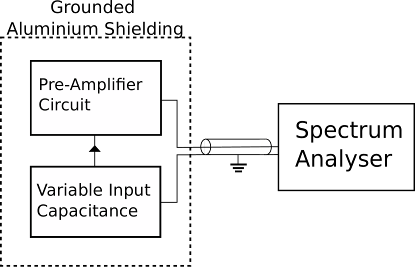
In this section the variable input capacitance and pre-amplifier circuits are located on the same circuit board and within the same aluminium shielding. In Section IV, however, these two parts are separated as described in that section.
III.1 Benchmark Circuit
A standard transimpedance circuit acting as a capacitive sensor is shown in Figure 4
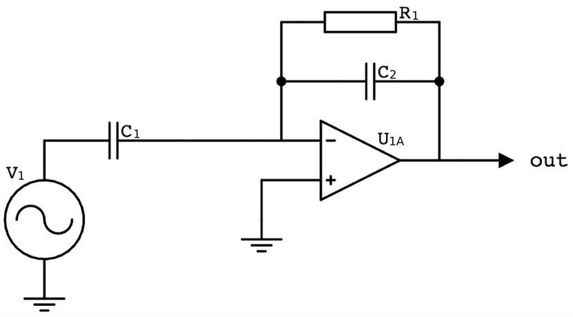
where the voltage generator, , connected to a changing capacitance , produces a current input signal for the op-amp . The absence of stray-capacitance means that this circuit can be considered to be a benchmark in terms of noise. The feedback network consists of a resistor and capacitor in parallel.
The output voltage noise from this circuit can be modelled by taking into consideration the main sources of noise present. These are the thermal noise from the feedback resistor , , the current noise density of the op-amp being used, , and the op-amp’s voltage noise density, , which is multiplied by the noise gain of the circuit, .
Noise gain in general can be changed without modifying signal gain. The noise gain for this benchmark circuit is described by the following equation
| (3) |
where as usual is . The total output voltage noise, (), is then given by the equation Amp (1992)
| (4) |
where the amplitude spectral density of Johnson noise in the feedback resistor is given by the usual expression Horowitz and Hill (1989)
| (5) |
is a one-pole low-pass filter term created by resistor and capacitor which acts to attenuate the Johnson noise produced by resistor and any signal at frequencies above the pole of the filter . In our measurements was chosen to be , but in practice the capacitance measured across varied between and due to the capacitances present on the circuit board used, leading to the reduction in measured noises at higher frequencies. The models used in this paper reflect these measured values. This simple analysis ignores the effects of the finite bandwidth of the op-amp, where the open-loop gain reduction at high frequencies must be taken into account. This, however, is acceptable in this case as the noise gain here is not affected by the smaller open-loop gain at high frequencies. Jung (1980)
The analytical expression for the voltage noise of this circuit in Equation 4 was compared to a direct measurement. In the voltage noise measurement, and all other noise measurements described in this paper, a Hewlett-Packard 35665A Dynamic Signal Analyser was used to measure the voltage noise directly from the output of the circuits. In order to eliminate as far as possible environmental background noise, the circuits under test were contained in aluminium boxes of wall thickness’s of approximately and were powered by batteries. The circuit was designed to optimise the noise performance for our displacement transducer ignoring the effects of any stray-capacitances.Chalkley et al. (2011) This leads to a design with low current noise and therefore large values of feedback resistance . The following component values were chosen for the benchmark circuit: capacitor was , was , the resistor was and the op-amp used for was a LTC6244HV. These values approximately match those that will be used in the detection circuitry for the capacitive sensor in the experiment where the modulation frequency is set to .Chalkley et al. (2011) The measurement and model are compared in Figure 5.
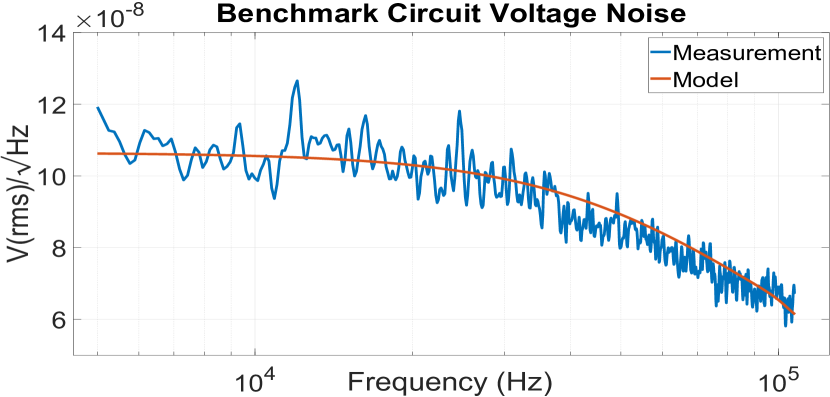
At the voltage noise is approximately .
It is interesting to note that there is a peak in the noise plot in both Figure 5, and later in Figure 13, at about 12kHz and must be due to some residual leakage of RFI into the set-up shown in Figure 3. Our models only look at the voltage noise inherent in the circuits alone as the Equations 3-5 suggest, and so we are not expecting to be able to predict and model the local interference in our laboratory. Despite this, the simple analytical model describes the noise well.
III.2 Stray-capacitance Circuit
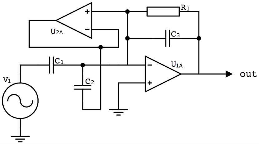
As a first attempt to model the effect of the stray-capacitance due to a cable we use a capacitor, labelled , which is connected to ground as shown in Figure 6.
We refer to this circuit as circuit B. The noise gain for circuit B is altered from that of the circuit in Figure 4 as the input impedance now comes from capacitors and in parallel. An equivalent noise circuit for the noise gain in Figure 6 is shown in Figure 7.

The noise gain for the circuit in Figure 6 is given by the following
| (6) |
In general and this leads to a large increase in noise gain. Inserting this new noise gain into Equation 4 gives an analytical expression for the voltage noise for circuit B. Unlike the case of the benchmark circuit in Figure 4, the finite bandwidth of the op-amp was taken into account here Jung (1980). This predicted noise was compared to direct measurement using the method mentioned previously. In measuring the noise of circuit B, repeated components from Figure 4 were kept the same and was which matched approximately the stray-capacitance of coaxial cable of the type used in our experiment at a length of . The measurement and model are compared in Figure 8.
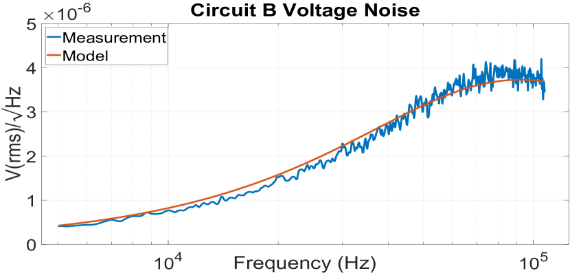
At the voltage noise is approximately . The simple analytical model describes the noise well.
III.3 Buffer Op-Amp Feedback Circuit
A common method for reducing the effects of stray-capacitance is shown by the circuit in Figure 9
labelled circuit C.Huang et al. (1988); Marioli, Sardini, and Taroni (1993) In this situation a buffer op-amp, labelled , is used in a feedback loop to drive both sides of the capacitor, , to the same voltage. In principle this should remove the effects of stray-capacitance. While this method has been shown to eliminate the bias capacitance due to the cable and the instability in circuits with large stray-capacitances, depending on the choice of op-amps used, Reverter, Li, and Meijer (2006); Spinelli and Reverter (2010) it does not improve noise performance.
The output noise of circuit C was measured using the method mentioned previously; the component values and types were identical to those in Figure 6. The buffer op-amp was initially chosen to be an OP07. An analytical model for the voltage noise at the output of this circuit can be derived by considering the noise introduced across capacitor from the op-amp in Figure 9. The total voltage noise, (), introduced is given by the equation
| (7) |
where is the buffer op-amp’s voltage noise in units of (), and is the impedance of capacitor . is the resistance value in the circuit and is the low-pass filter term from Equation 4 which at is 0.55. In practice the pole of would be at higher frequencies where it would not attenuate any signal.
The voltage noise measurement and model are shown in Figure 10.
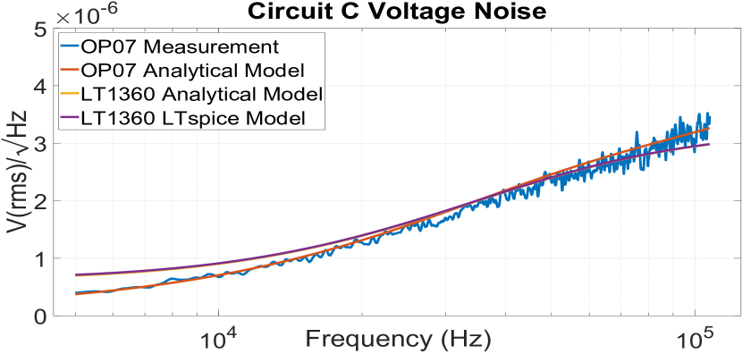
At the voltage noise is approximately . Also shown in Figure 10 is the analytical model and LTspice result for the LT1360, as , which is an operational amplifier with a faster slew rate and lower voltage noise density than the OP07. Using this op-amp the voltage noise is reduced to approximately at . The analytical model describes both the measured and LTspice predicted noise spectra well.
This analysis shows that the presence of the buffer op-amp can contribute a significant amount of output voltage noise to the circuit, as the stray-capacitance, , will couple the noise to the signal carrying core. Rich (1983) It also suggests that the similarity between the noise measurements in Figures 8 and 10 is coincidental. Where for Figure 8 the increased noise comes from the op-amp voltage noise being multiplied by the large noise gain, and for Figure 10 it arises from the feedback op-amp voltage noise being introduced across the stray-capacitance.
III.4 Proposed Noise Gain Modification Method
Figure 10 shows clearly that the conventional solution to the problem of stray-capacitance, which although allows a circuit to operate in a stable and accurate manner, gives an increased voltage noise. The goal is then to reduce the effects of stray-capacitance on the stable operation of a transimpedance circuit, while maintaining as low a circuit noise as possible compared to the benchmark circuit.
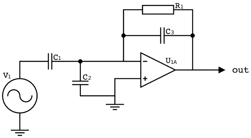
One way to do this is to reduce the noise gain of the circuit. This can be done by using the set-up shown in Figure 11,
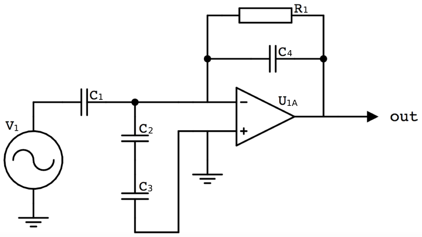
whose equivalent noise circuit for the noise gain is shown in Figure 12.

In this circuit, labelled circuit D, the signal gain is the same as for the benchmark circuit in Figure 4, but now the noise gain is altered from Equation 6 to the following
| (8) |
This change is due to the introduction of the capacitor labelled , which is in series with the stray-capacitance . If , then Equation 8 reduces to Equation 3 which is the benchmark best-case scenario.
When this new noise gain is used with the general noise formula given in Equation 4, we obtain an expression for the voltage noise of this new circuit. The noise of circuit D was measured using the method mentioned previously. Repeated components from Figure 6 were as before and was . The measurement and model are compared in Figure 13.
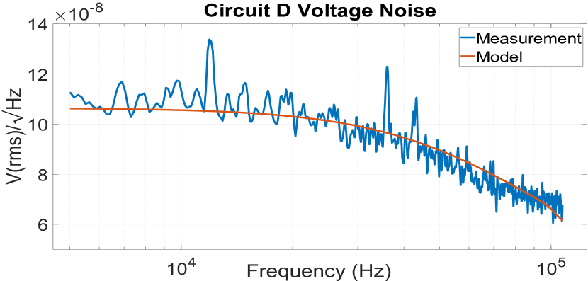
At the voltage noise is approximately . As with the previous noise measurements, the model matches the measured voltage noise well.
IV Shield Effectiveness
For our candidate circuits it is important to quantify the effectiveness of the coaxial cable in shielding the signal carrying wire from environmental electromagnetic interference. This was done using circuits B and D, as circuit B is the typical shielded scenario and circuit D represents our method where the shield is now floating with respect to ground and as such is less effective. The in-situ cables in our experiment were attached to the inputs of these two circuits whilst they were located in our laboratory. This allowed a direct comparison of the output noise to be made under lab conditions. A measurement was also made with the benchmark circuit but with an unshielded cable at the input to the op-amp, to give a reference noise for the background interference. A very important feature to note here is that the majority of the length of cables involved were inside a large metallic cryogenic dewar (which was electrically floating with respect to the circuits under test through a capacitor to ground) which would have provided extra shielding regardless of whether the coaxial shield was floated or not. This is typical for any cryogenic experiment and so is a fair comparison.
These measurements, along with the test measurement of circuit D from Figure 13 for comparison, are shown in Figure 14.
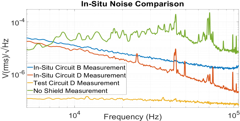
This figure shows that although there are significant interference noise peaks at certain frequencies for the in-situ circuit D, overall there is a much lower noise floor compared to the in-situ circuit B implying that the lowering of noise gain is worth the reduction in electromagnetic interference shielding. Also the no-shield scenario is shown to be a non-viable alternative to the problem of parasitic capacitance from shields. At the in-situ circuit D noise is approximately 3.1 times larger than the test circuit D case. Aside from interference, additional noise creating this disparity between scenarios could arise from unaccounted for parasitic capacitances within the experimental set-up. As already stated, our set-up of course benefited from the fact that for the in-situ measurements, the majority of the cabling was contained inside a cryogenic dewar, which would have provided additional shielding.
V Summary
| Circuit | Voltage Noise | Disp. Noise |
|---|---|---|
| Benchmark Circuit | ||
| Circuit B | ||
| Circuit C OP07 | ||
| Circuit C LT1360 | ||
| Circuit D | ||
| In-Situ Circuit B | ||
| In-Situ Circuit D | ||
| In-Situ No-Shield |
A summary of the voltage noises at for the benchmark circuit, and circuits B, C and D from Figures 4, 6, 9 and 11 respectively, is listed in Table 1. The same is done for the in-situ circuits B and D as well as the no-shield circuit from Figure 14 for comparison.
These noise values have been converted into displacement noises in the table. This is to highlight the projected physical sensitivities of these circuits based on the specifications of our experiment, where we have a bias AC drive voltage of , a capacitor plate separation of the order of in the capacitive transducer bridge and a capacitive plate area of .
VI Discussion
The voltage noise from a variety of pre-amplifier circuits for non-resonant capacitive sensors has been measured and modelled in order to explore the negative effects of large stray-capacitances at their inputs. Five different test circuits were compared: one was a standard pre-amplifier that was optimised for our application with no stray-capacitance (Benchmark circuit); one was the standard pre-amplifier but now with stray-capacitance (circuit B); another two employed active feedback to maintain the cable shield at the voltage of the input to the op-amp (circuit C using two different amplifiers for the active feedback). Finally, a novel circuit (circuit D) was tested. A summary of the noise characteristics of these circuits is shown in Table 1. Circuit D had the best noise characteristics, along with the benchmark circuit, and is shown in Figure 11. The addition of a simple small capacitance, , connecting the shield to the non-inverting input of the pre-amplifier reduces the noise gain that is produced by the low impedance of the shield. The voltage noise for this circuit is shown in Figure 13.
In-situ results indicate a modest increase in noise, by a factor of 3, due to environmental interference and the non-static capacitances present in our actual set-up. This increase is, however, still acceptable at the signal modulation frequency of . This indicates environmental interference is relatively benign in this situation and so the reduced shield effectiveness is not significant in this case. In our experiment this is due to the fact that the signal carrying coaxial cable is mostly inside a cryogenic dewar which is effectively a Faraday cage and a shield against high frequency magnetic fields. Clearly standard modulation/demodulation schemes can mitigate against low frequency interference if it does not overwhelm the pre-amplifier. The degradation in the measured shielding effectiveness is not equivalent to there being no shield at all, as shown in Figure 14.
VII Conclusion
The proposed circuit is a trivial extension of the usual methods of designing a capacitive sensor circuit. However, as far as we are aware, it has not been proposed previously most likely due to the perception that it is incapable of providing shielding from environmental interference. The proposed technique could be successfully employed in many applications in addition to cryogenic experiments. For example, vacuum systems are employed in many sensitive experiments and would provide electromagnetic shielding from external noise sources. In general, however, there may be situations were interference is a dominant factor that determines a capacitive sensor’s sensitivity. A particularly important case is when an unshielded drive signal at the input of a bridge circuit ( in Figures 4, 6, 9 and 11) can couple directly to the pre-amplifier. In such cases a method for which the shield effectiveness is preserved should be employed.
One way to balance the benefits of a decrease in noise gain with the negatives of a reduction in shield effectiveness may be to make capacitor from Figure 11 a variable capacitor. This could allow the trade-off to be fine-tuned for more general applications, and may be a more general solution to the problem of stray-capacitance when external interference cannot be ignored and where fine cables are required to minimise the heat leak in a cryogenic experiment. In our case, placing the pre-amplifier circuit near the point where the coaxial cable leaves the cryogenic dewar further reduced interference and drove the voltage noise closer to the ideal value.
Finally, it may be useful to the reader if we compare the performance of the capacitive sensor presented here with, for example, a resonant capacitive sensor. Bertolini et al. (2006) In general, the sensitivity of capacitive sensors is proportional to the bias AC drive voltage applied to the electrodes, and inversely proportional to the equilibrium separation distance between the two sensing electrodes. For the resonant bridge transducer these parameters are and respectively.Bertolini et al. (2006) Other factors such as capacitance plate area and drive frequency are important but strongly depend on each individual case as to what is practical. From Table I, the in-situ circuit D sensor has a displacement noise of that would be expected to be about after coherent demodulation, whereas the resonant bridge transducer has a noise floor of approximately above . Bertolini et al. (2006) We can estimate an approximate sensitivity of our detector if we employed the same gap and drive voltage as that for the resonant sensor. These parameters can be easily modified in our design. We then find that our device would be a factor of about 7 less sensitive. Nevertheless we believe the simplicity of the transimpedance scheme that we have presented here has its merits. Further our device has been demonstrated in a cryogenic setting and has sufficient sensitivity for our application. Chalkley et al. (2011)
Acknowledgements.
We would like to thank David Hoyland for many useful and constructive discussions. We are grateful to UK STFC (grant number: ST/F00673X/1) who initially supported this work. We are also very grateful to Leverhulme (grant number: RPG-2012-674) for financial support. We would also like to Stefan Schlamminger for refocussing our efforts toward a capacitive sensing solution for our experiment.References
- Jones and Richards (1973) R. V. Jones and J. C. Richards, Journal of Physics E-Scientific Instruments 6, 589 (1973).
- Smith and Seugling (2006) S. T. Smith and R. M. Seugling, Precision Engineering-Journal of the International Societies for Precision Engineering and Nanotechnology 30, 245 (2006).
- Chatterjee et al. (2017) K. Chatterjee, S. N. Mahato, S. Chattopadhyay, and D. De, Instruments and Experimental Techniques 60, 154 (2017).
- Oven (2014) R. Oven, IEEE Transactions on Instrumentation and Measurement 63, 1748 (2014).
- Ramanathan et al. (2016) P. Ramanathan, S. Ramasamy, P. Jain, H. Nagrecha, S. Paul, P. Arulmozhivarman, and R. Tatavarti, in Sensors, Transducers, Signal Conditioning and Wireless Sensors Networks, Advances in Sensors-Reviews, Vol. 3, edited by S. Yurish (Int Frequency Sensor Assoc-IFSA, C/Esteve Terradas, Parc UPC-PMT, Edifici RDIT-KAM, 1, Barcelona, Castelldefels 08860, Spain, 2016) pp. 213–227.
- Bertolini et al. (2006) A. Bertolini, R. DeSalvo, F. Fidecaro, M. Francesconi, S. Marka, V. Sannibale, D. Simonetti, A. Takamori, and H. Tariq, Nuclear Instruments & Methods in Physics Research Section A - Accelerators Spectrometers Detectors and Associated Equipment 564, 579 (2006).
- Hu et al. (2014) M. Hu, Y. Z. Bai, Z. B. Zhou, Z. X. Li, and J. Luo, Review of Scientific Instruments 85 (2014), 10.1063/1.4873334.
- Amp (1992) Amplifier Reference Manual (Analog Devices, Inc., 1992).
- Horowitz and Hill (1989) P. Horowitz and W. Hill, The Art of Electronics, 2nd ed. (Cambridge University Press, 1989).
- Jung (1980) W. G. Jung, IC Op-Amp Cookbook, 2nd ed. (Howard W. Sams & Co., Inc., 1980).
- Chalkley et al. (2011) E. C. Chalkley, S. Aston, C. C. Collins, M. Nelson, and C. C. Speake, in Rencontres de Moriond and GPhyS Colloqium 2011 (2011).
- Huang et al. (1988) S. M. Huang, A. L. Stott, R. G. Green, and M. S. Beck, Journal of Physics E: Scientific Instruments 21, 242 (1988).
- Marioli, Sardini, and Taroni (1993) D. Marioli, E. Sardini, and A. Taroni, Measurement Science and Technology 4, 337 (1993).
- Reverter, Li, and Meijer (2006) F. Reverter, X. Li, and G. C. M. Meijer, Measurement Science and Technology 17, 2884 (2006).
- Spinelli and Reverter (2010) E. M. Spinelli and F. Reverter, IEEE Transactions on Instrumentation and Measurement 59, 458 (2010).
- Rich (1983) A. Rich, Analog Devices 17, 8 (1983).