A Flexible FPGA Accelerator for Convolutional Neural Networks
Abstract
Convolutional neural networks (CNNs) have become popular for machine perception tasks on images and videos including image classification, object recognition, and medical diagnosis. The desire for high performance and power efficiency while running CNNs has led to an explosion in specialized hardware accelerators. FPGAs provide a promising alternative to ASICs and GPUs for flexible hardware acceleration: reconfigurability makes them attractive on the Cloud for a wide range of users whose requirements on precision and other aspects are likely to be different.
Though CNNs are highly parallel workloads, in the absence of efficient on-chip memory reuse techniques, an accelerator for them quickly becomes memory bound. In this paper, we propose a CNN accelerator design for inference that is able to exploit all forms of reuse available to minimize off-chip memory access while increasing utilization of available resources. The proposed design is composed of cores, each of which contains a one-dimensional array of processing elements. These cores can exploit different types of reuse available in CNN layers of varying shapes without requiring any reconfiguration; in particular, our design minimizes underutilization due to problem sizes that are not perfect multiples of the underlying hardware array dimensions.
A major obstacle in the adoption of FPGAs as a platform for CNN inference is the difficulty to program these devices using hardware description languages. Our end goal is to also address this, and we develop preliminary software support via a codesign in order to leverage the accelerator through TensorFlow, a dominant high-level programming model. Our framework takes care of tiling and scheduling of neural network layers and generates necessary low-level commands to execute the CNN.
Experimental evaluation on a real system with a PCI-express based Xilinx VC709 board demonstrates the effectiveness of our approach. As a result of an effective interconnection, the design maintains a high frequency when we scale the number of PEs. The sustained performance overall is a good fraction of the accelerator’s theoretical peak performance, and to the best of our knowledge, higher than previously published open designs with a similar setup.
I Introduction
Convolutional neural networks have enabled rapid progress in the fields of image classification [10, 32], object recognition [24, 5, 25], medical diagnosis from scans [26], and speech to text translation. All of these fields fall into the field of machine perception involving images, video, and speech. Besides delivering high accuracy, the simple and regular characteristics of the computation have allowed system designers — all the way from architects, high-performance library and compiler developers, to programming model designers — to optimize and accelerate these computations in turn leading to further innovation. This has created a highly desirable self-reinforcing feedback loop over the past seven years. CNNs have been deployed on a vast range of platforms from data-centers to mobile phones.
While CNNs have high compute requirements, multi-core CPUs and GPUs have proved to be efficient for training neural networks as a result of how well the underlying matrix-matrix multiplication-like patterns have been optimized to run at close to peak performance [6, 30, 16]. However, most inference workloads have strict latency and power budgets. Although ASICs can be used to implement high performance, power-efficient CNN accelerators, but they are not very cost effective in the absence of a high volume demand.
FPGAs provide a good compromise between cost effectiveness, performance and power efficiency. With a significant amount of computing moving to the Cloud, FPGAs are also attractive in that they could be customized to the varied requirements of the multiple users a cloud server will have to support. Such requirements could stem typically from precision, but also from other aspects such as the CNN model itself and the problem sizes. While reconfiguring an FPGA while executing a particular user’s workload may not be a practical choice, providing a customized accelerator for a particular user is quite appealing.
Designing an FPGA-based custom accelerator for CNNs is a difficult task, and domain experts obviously should not have to think about hardware-specific complexities involved. CNNs have abundant parallelism and the performance of a hardware implementation, with sufficiently high compute power, could be predominantly limited by available off-chip bandwidth if on-chip date reuse is not effective. CNNs offer multiple data reuse opportunities such as input feature map reuse along output channels, weight reuse within an input-output channel pair, partial output sum reuse along the input channel dimension, and convolutional reuse of both inputs and partial sums. Exploiting available data reuse is essential for a high performance accelerator design. In addition, CNNs offer other optimization opportunities such as reduced precision computing and sparsity in input and weights. In this work, we primarily focus on data reuse while keeping the option of utilizing sparsity and reduced precision computing open for future work. We describe the design and evaluation of an FPGA-based CNN accelerator. We also build out the corresponding software support to utilize the accelerator by leveraging it from high-level programming models like TensorFlow.
The ability to exploit available data reuse opportunities is heavily influenced by the arrangement of processing elements (PEs), the design of the on-chip interconnect [15] connecting the PEs, and the associated dataflow techniques [4]. Different layers of a CNN can have very different shapes and can thus offer better data reuse along different dimensions. To effectively exploit data reuse along multiple dimensions, previous work has explored two-dimensional arrays of processing elements (PEs) [4, 13, 28]. The dimensions of these two-dimensional arrays must be carefully chosen to reduce under-utilization due to problem sizes that are not multiples of the underlying processor array dimensions. An accelerator may use flexible interconnect design [15] or more complex mapping techniques [4] to improve utilization of processing elements and data reuse, but the added complexity contributes to increased area and power consumption.
Our design constitutes multiple cores, where each core is a one-dimensional array of processing elements (PEs). Each core can perform a convolution operation of a single CNN layer or tiles of it if the former does not fit within the resource constraints. One of the characteristics of our design is that the under-utilization due to the cleanup part of the problem size is minimized due to the flexibility of mapping to the 1-d array. A tile of an arbitrary shape can be linearized to map to our 1-d PE array. All of this is achieved while not compromising on data reuse available along multiple dimensions.
In summary, our contributions are as follows.
-
•
We develop a CNN accelerator architecture that comprises multiple cores where each core is a one-dimensional array of processing elements. We show that a carefully designed one-dimensional design can obtain better utilization compared to 2-d designs. Also, the architecture can independently scale with available bandwidth and compute resources of an FPGA.
-
•
We show that the proposed accelerator exploits data reuse along all dimensions.
-
•
We exploit known data access patterns of CNNs to design a scalable and lightweight interconnect (in terms of resources) for transferring inputs to PEs.
-
•
We develop a software framework to automate the process of running CNNs on FPGA.
The rest of this paper is organized as follows. Section II provides the necessary background on CNNs and the computational characteristics to the extent they are relevant in designing parallel accelerators. Section III describes our core architecture in detail along with an analysis on how it exploits resources and properties of the computations targeted in Section IV. Section V describes the software stack to make the accelerator usable with high-level programming models. Section VI presents our experimental evaluation Section VII describes related work, and conclusions are presented in Section VIII.
II Background: Convolutional Neural Networks
In this section, we provide the relevant background on CNNs and the convolution operation.
A CNN is a feed-forward neural network containing multiple layers. The input and output of a layer are three-dimensional tensors (ignoring batching). Each layer computes a convolution operation, an elementwise activation operation and an optional max-pooling.
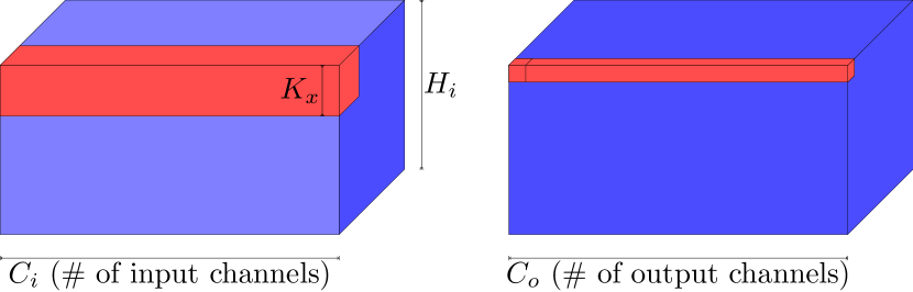
A convolution is the most compute heavy operation in a CNN. Figure 1 shows a convolution layer with inputs and outputs. A three-dimensional input tensor is convolved with a four-dimensional weight tensor to calculate the output. The calculation of a single output value can be represented as follows:
where is the input tensor (also called the input feature map or the input channels) of shape , is the output tensor (output feature map or output channels) of shape , and is the weight tensor of shape . and denote the number of input and output channels respectively, while and are the width and height of a single channel of the input, (similarly and for output channels) and , represent the convolution window size.
A single convolution operation exhibits the following types of data reuse:
-
1.
input reuse: Each input value contributes to the calculation of outputs (assuming unit stride);
-
2.
weight reuse: Each weight value is reused for calculating output values (corresponding to a single input()-output() channel pair);
-
3.
partial sum reuse: Each output is calculated as a multiply accumulate operation of input and weight values. Hence, the partial sum (psum) is reused times during this operation.
Depending on the shapes, some CNN layers could have a higher input and psum reuse, while others could have a higher weight reuse. Strides greater than one reduce input reuse. In order to achieve a high utilization of PEs in the computation of each CNN layer, an architecture must be able to maximize reuse along all dimensions.
III Architecture
In this section, we describe the core architecture of our proposed accelerator design along with a detailed discussion of its characteristics, strengths, and limitations.
Figure 2 gives a high level overview of our architecture. Our accelerator is composed of one or more cores. Each core contains multiple processing elements (PEs). A processing element is the smallest compute resource in our design. Each processing element contains one scalar fused-multiply-accumulate unit. In addition, PEs are provisioned with local scratchpads to cache inputs, partial and final outputs. Each core contains three interconnects to transfer inputs and weights to PEs and to read back computed output. Each of these interconnects has the capacity to transfer one value every cycle. A centralized controller within each core orchestrates dataflow and generates control signals to schedule computation on the array of PEs.
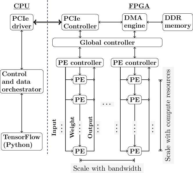
Based on the available bandwidth and compute resources, the exact number of cores and PEs per core can be decided. As mentioned before, each interconnect within a core can transferring one value every cycle. Thus, maximum bandwidth that a single core can utilize is limited by the capacity of these interconnects. Since, each core has a fixed peak bandwidth requirement, the total number of cores is calculated by dividing available bandwidth (in the FPGA) with the bandwidth requirement of one core. Number of PEs per core is limited by available resources in the FPGA. Thus, our templated design scales with bandwidth (by increasing number of cores) and compute (by increasing number of PEs) independently.
III-A Core
Each core can compute convolution between a three dimensional input feature map and a four dimensional weight tensor to calculate a three dimensional output. Listing 1 shows the pseudocode for this computation. Loop nest x, y is parallelized by distributing it among PEs, each PE responsible for executing one iteration of the loop nest. The operations within each PE can be broken into three parts, input read (loops m and n), computation (loops i, j, co, ci) and output write back (loop t). The input read of the next channel and the output writeback of the previous convolution are overlapped with the current execution to hide data transfer latency. The convolution operation scheduled to a core must fit the available resources. must be less than or equal to total number of PEs in the core and the number of output channels must be less than the output buffer size. The input is double buffered to hide data transfer latency; hence it must be large enough to hold two windows of the input feature map. A convolution operation that does not fit inside a core can be tiled along , and dimensions such that each tile fits the core. Such tiling is done by the software runtime. The host side software communicates with the core via PCIe to schedule convolution operations.
III-B Processing element

Each core contains a one-dimensional array of processing elements. Figure 3 shows the internals of a PE. A PE is the smallest compute unit in our design. Each PE can perform one multiply-accumulate operation every cycle. Partial outputs are cached within the PE and only the final outputs are sent back. PEs do not have any controller and all control signals are sent by core’s controller. As discussed earlier, PEs overlap output writeback and input read with current computation to avoid stalling. If the data transfer latencies are less than the compute time, a PE will never stall. Each PE contains one MAC unit and scratchpad memory for inputs, partial sums and outputs. In addition, a PE has a receiver and a sender node. A receiver decides which data from the input interconnect will be cached. A sender is responsible for reading the output buffer and sending out the value via an interconnect.
Inputs and partial sums are cached to exploit temporal reuse within a PE. Outputs are buffered to overlap the output read of a previous convolution with current compute. As shown in Listing 1, weights are reused across PEs but there is no weight reuse within a PE. Hence, weights are not cached. A PE calculates all feature channels corresponding to one pixel in the output feature map using inputs cached in its local buffer. In our current design, the input buffer is a 32-entry FIFO implemented using distributed RAM. Output and partial output buffers are 512-entry FIFOs realized with block RAMs. As can be seen in Listing 1, loop x and y are distributed among PEs, and only PEs are active during a convolution operation. Hence, must be large for high utilization of PEs within a core. is also the total amount of weight reuse.
III-C Core controller
The core controller is responsible for sending input and weights through the interconnects, signaling PEs to perform the computation and reading back outputs. It receives commands from the software runtime with the convolution parameters. The controller then generates micro-instructions to control data transfer and computation. It inserts appropriate stalls when the computation time cannot completely hide data transfer time.
III-D Interconnect Design
The performance of an accelerator heavily depends on the ability of the on-chip interconnect to efficiently transport required data to the compute resource. Without timely supply of data, these resources will stall, impacting overall performance. Additionally, interconnects must be lightweight to ensure sufficient FPGA resources are left for other parts of the design such as compute. In our design, each core has three interconnects to transport inputs, weights and outputs respectively. These interconnects can be classified as unicast, multicast and broadcast. The output interconnect is responsible for collecting outputs from PEs and is a unicast interconnect. In each cycle only a single PE is sending its output back to the core controller. The input interconnect is multicast as it needs to send one input to PEs. Each sent weight is required by all PEs, and hence, is transported via a broadcast interconnect. All these interconnects are pipelined to meet the desired frequency. Next we discuss the mechanism by which each interconnect communicates with the PEs. The output interconnect forwards read requests from the controller to all the PEs. Each PE responds to this request by sending one value from its output buffer back to the controller via the interconnect. Since the interconnect is pipelined, PEs do not overwrite each others’ output.
The weight interconnect is the simplest of the three. Weights are sent by the controller. Each PE uses the weight for updating its partial outputs and in the subsequent clock cycle, forwards it to the next PE .
| Command | Operation |
|---|---|
| 13 | Start (First input) |
| 0 | No op |
| 1 | DilateX |
| 2 | ErodeX |
| 3 | ShiftX |
| 4 | RotateY |
| 5 | DilateY |
| 6 | ErodeY |
| 7 | ShiftY |
| 8 | Intermediate cmd for ShiftX |
| 9 | Intermediate cmd for DilateX |
| 10 | Intermediate cmd for ErodeX |
| 11 | Intermediate cmd for DilateY and ShiftY |
| 12 | Intermediate cmd for DilateY and ShiftY |
| Initial state | Command Change | Final state |
|---|---|---|
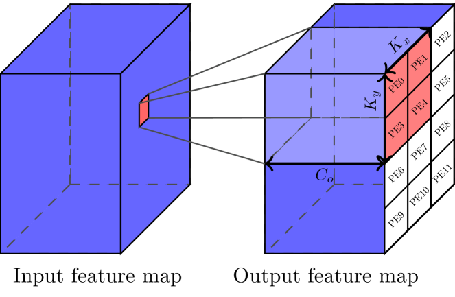
The input interconnect is more complex because an input may be received by a subset of PEs. Each input is cached by PEs for weight tensor of size . The PEs that cache an input are not arbitrary and for consecutive input values these receiving PEs change in a specific patterm. Instead of using a general purpose multicast interconnect, we exploit this pattern for a more lightweight design. In order to understand how the PEs that cache an input change with consecutive values along a row or column of input feature map, we rearrange the one dimensional array of PEs as a logical two dimensional array (as shown in Figure 4(b)) of size for an output of dimension .
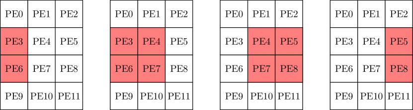
Each PE contains a receiver through which connected to the input interconnect. A receiver contains two one bit flags, RD and LS, which together constitute is state. RD indicates that the receiver is active and will read data from the interconnect. LS indicates that it is the first PE in a row that contains active receivers. In other words, LS indicates the start of rows that contain active receivers.
We define the term receiver PEs, for a given input value, as the set of PEs that need to cache this value in their input buffer. For unit stride, each input value (except at boundary) contributes to outputs as shown in Figure 4(a), where is the number of output channels. Figure 4(b) shows how the receiver PEs change for input values in a row (assuming unit stride and weights) of an input channel. Receiver PEs for the second input value dilates one extra column to the right compared to the first value. From second to third value, the receiver PEs shift horizontally and from third to fourth value it erodes one column from left. Note that, even with non unit strides, receiver PEs can never change more than one column in left or right direction for consecutive input values of a row. Hence, change in receiver PEs for consecutive input values of a row, can be expressed using three primitive operations of dilation, shifting and erosion along x-axis. Furthermore, for non unit strides, two adjacent inputs of a row may have same receivers.
The input interconnect carries a 4-bit command in addition to data. The receiver, upon receiving a command updates its state (RD and LS bits) and forwards a new command to the next PE. Table I(b) shows the output command and updated state for a given input command and previous state. Table I(a) lists all the commmands. Based on the convolution window size and stride values, the controller sends commands, such as DilateX or ShiftY, to update the set of receivers that will cache the next input. The resource overhead of input interconnect consists of a 4 bit command bus to carry the command and the logic to implement Table I(b) in each PE, which is very small and scales linearly with number of PEs.
III-E Support for different precisions
The current implementation of our architecture supports both single precision floating point and 8-bit integer multiply with 32-bit accumulate. In this section, we discuss certain unique challenges for the int8 configuration and how we address them.
In order to implement int8 operations (8-bit inputs, 8-bit weights and 32-bit accumulation for output), we vectorize the PE. Thus, instead of doing one 32-bit floating point multiply-accumulate operation, each PE now performs four 8 bit integer multiplications and additions per clock. The software runtime packs a set of four inputs into one 32-bit value. The dimensions we choose to pack into a vector can have a significant impact on the design. One obvious choice is to take sets of four batches and pack them together. This way, the core would simultaneously be performing a convolution on four batch samples. The problem with this approach is that int8 requires 32-bit accumulation. This means that even though the inputs and weights are 8-bit wide, we will have to store the partial outputs from all four batches in 32-bit precision. This increases our block RAM usage by nearly four times.
vPE: To address this issue, we choose to pack four input channels into one vector (and corresponding weight channels into one weight). Each processing element calculates one dot product of the four packed inputs and weights (while using 32 bit accumulators). This generates only one 32 bit partial output (as opposed to four 32-bit partial outputs in the previous case). The block RAM usage remains the same as with FP32, while we perform four multiplies and four adds instead of one floating point multiply-accumulate. The trade-off is that we exploit reduction parallelism along the input channel dimension (four multiplies followed by an adder tree of three adds and an add to accumulate) to generate the single reduced 32-bit output. Instead of calling this 4-way parallel compute unit a PE, we refer to it as vPE here on.
IV Data Reuse and Utilization
In this section, we describe how the proposed design exploits reuse in order to achieve high performance and scale with resources.
Convolutional neural networks are highly parallel workloads. Each output calculation is independent of others. In addition, there are parallelization opportunities within the calculation of one output. Despite this, performance cannot scale by merely increasing the amount of compute resources. This is because the amount of performance that an accelerator can achieve is limited by its ability to keep the compute units busy, i.e. utilization of the available compute power. In order to achieve a high utilization, an accelerator must exploit various data reuse opportunities present in convolution operations.
On-chip data reuse is defined as the number of times a data participates in a computation before being discarded. Section II described the input, output and weight reuse available in a convolution operation. Each convolution operation has an input reuse of , weight reuse of and output (partial sum) reuse of .
In order to analyze different kinds of on-chip reuse and the utilization of compute resources, we make following assumptions:
-
1.
The output feature map dimensions have been tiled such that num PEs, and output buffer size for an output tile of size . We also assume that input buffer size.
-
2.
The available bandwidth is enough to feed one input and weight to the core and read back one output from the core every cycle. We assume that bandwidth allocated for input cannot be traded for weight. This is because our design contains separate interconnects for inputs and weights that can send at most one input and one weight every cycle.
We now describe how our core exploits reuse. A unique property of our accelerator is that it does not have any global scratchpad and all reuse is either within a PE or due to sharing among PEs. Based on this observation, we classify the on-chip reuse into following two categories:
-
•
Intra-PE reuse is the temporal reuse of data cached in local scratchpads of a PE. The amount of reuse is equal to the number of times a data is accessed from the local scratchpad before being overwritten.
-
•
Inter-PE reuse is the shared use of any data among multiple PEs. This constitutes any data that is sent to multiple PEs through the interconnects. The number of PEs that use a given data, defines the amount of its reuse.
Input reuse is achieved through a mixture of inter-PE and intra-PE reuse. Since each PE caches a window of inputs from an input feature map, the number of PEs that cache the input is also equal to (except boundary pixels which are required by less PEs). This is a form of inter-PE reuse due to multiple PEs sharing same input. In addition, once cached, each value in the window, contributes towards updating partial sums, also cached in the PE. Thus, each input value has an intra-PE reuse of . In total, each input value is reused times. Since each weight sent through the interconnect is used by every active PE, the weight reuse is equal to the number of active PEs, . This reuse is completely inter-PE reuse. Since weights do not have intra-PE reuse, they are not cached in PEs unlike inputs and partial outputs. Partial sums remain in a PE’s local scratchpad until final outputs are calculated. As can be seen in Listing 1, each partial sum participates in multiply accumulate operations before the final outputs are ready. Thus, partial sum reuse is completely intra-PE reuse and is of factor .
Thus, all of the available reuse for inputs, kernel and outputs, is either exploited within local buffers of PEs or among multiple PEs without needing a global buffer.
IV-A Utilization of PEs
The utilization of available compute resources places an upper limit on the peak achievable performance. In this section, we develop an analytical model to estimate the theoretical maximum utilization of PEs in a single core of our design. We build this model with the previously defined assumptions that the convolution operation is tiled to fit the core and that there is enough bandwidth to supply one input and weight every cycle and read back one output.
We categorize the utilization of PEs into two distinct types.
-
•
Spatial utilization: Since each PE calculates all channels corresponding to one output pixel, if the number of output pixels, , is less than the number of PEs, then some PEs will remain inactive for the current operation. We call the ratio of number of active PEs to the total number of PEs as spatial utilization because it shows how many PEs are active for the duration of the convolution.
-
•
Temporal utilization: We use double buffering of inputs and outputs to overlap compute time with data read/write time. This ensures that PEs do not stall waiting for the input read or output writeback. However, if the input read or output writeback time is more than the compute time, the active processing elements will begin to stall waiting for the input or for output buffer to become available. We call the ratio of compute time to the maximum of input read time and output writeback time as the temporal utilization since it indicates the fraction of time the active PEs perform useful computation. Since weights are used by all PEs and we previously assumed that we have a bandwidth to transfer at least one weight per cycle, PEs cannot stall due to weights.
Spatial utilization is defined by:
where is the number of processing elements in a core and the output feature map is of size . Note that is always less than equal to one because we cannot schedule a convolution operation on the core that has .
Listing 1 shows the number of computations sequentially executed by one PE. Since we read one input per cycle, the time required to read one channel of input feature map is . Each PE caches window of this feature map and updates the partial outputs. It takes cycles to update all the partial outputs using this window. Thus in order to keep the PEs busy all the time, input read time must be less than the compute time. In case input read time is more, the PEs will stall for the remaining cycles waiting for inputs to arrive. Thus, gives an upper bound on temporal utilization. Similarly the time required to send back all outputs is . Hence, temporal utilization is given by the formula:
The upper limit on is reached when compute time is equal to or more than the input/output read/write time.
The total utilization of a core is given by which is equal to
When the output feature map is larger than the total number of PEs, we tile it to fit the core.
V Software Framework
In this section, we describe the software stack that integrates the accelerator into the TensorFlow toolchain.

V-A Mapping linearized shapes to reduce under-utilization
Figure 6 shows our tiling strategy. We tile the and dimensions so that each tile is of size . If required, the output channel dimension, , can also be tiled. However, in our experiments, we did not have to tile the output channel dimension since the output buffer was large enough to fit all output channels. To make the tiling implementation simpler, we always keep the number of PEs a perfect square. Our architecture however has no restriction on the number of PEs. Assuming that the number of PEs is , we try to fit as many tiles as we can, starting from the top left corner. In Figure 6, this is shown by the tiles marked RR (R stands for regular-regular). This leaves us with two partial tiles RS (regular-small) and SR. Next, we attempt to schedule the RS tile. If the number of output pixels in the RS tile is less than the total number of PEs in a core, we can schedule the complete RS tile. Otherwise, we further divide it into smaller sub-tiles. A sub-tile will have the same width, as the RS tile. Note that . Thus we are guaranteed that we will be able to fit at least a sub-tile of size in the core. We divide the RS tile along the dimension (height) into sub-tiles, where each subtile is of size except the last tile which may be of height less than . Similarly, we break down the SR partial tile into subtiles along the dimension. The sub-tiles that originate from RS and SR can have a very skewed aspect ratio. For example, if we have 64 PEs per core and then, the partial tile SR will be of size , i.e., a one pixel wide column of output values. Our one-dimensional PE array design does not put any constraint on the aspect ratio of the scheduled tile. Hence, we can schedule the complete tile in the core (which has 64 PEs).
V-B Software stack
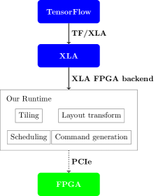
Figure 5 provides an overview of our software stack. The high-level description of a CNN is specified as a TensorFlow model, which is our starting point. Our runtime takes the input as an XLA HLO graph, an intermediate representation on the path of TensorFlow compilation. The runtime then performs the necessary data layout transformation on inputs, tiles each convolution layer to fit on the FPGA, and generates low-level instructions to schedule each tile on the FPGA.
Our design requires the layout of weights to be , while TensorFlow uses a layout of . Similarly, we need the input/output feature map layout to be , but TensorFlow’s default layout is (ignoring the batch dimension). Our runtime helper performs the necessary layout transformation. It then creates a schedule for executing tiles, packs the required input feature channels and weights, along with instructions to execute the convolution operation on the core, and sends this packet to the FPGA via PCIe. Upon receiving the results, the runtime unpacks the output to the correct layout and returns it to TensorFlow.
While the key contribution of this work is on the hardware side, our larger longer term goal is to build HLS support to it through a dialect in MLIR [19], which is an intermediate representation to which TensorFlow is moving, and which potentially other AI/ML compilers are likely to adopt.
VI Experimental Evaluation
In this section, we describe the experimental setup, the evaluation performed, and an analysis of the results. All performance and execution time measurements are from a real experimental system.
VI-A Setup and Methodology
We implemented our accelerator using Verilog. The experimental setup constitutes a Xilinx VC709 FPGA evaluation board connected over PCI-ex 3.0 (via an x16 interface) on an Intel Xeon E5-2630 v3 server (Intel Haswell-based) with 64 GB of DDR4-1600 RAM for experimental evaluation. All reported numbers are with Vivado 2019.1 being used for synthesis. Riffa [12] was used for host to FPGA communication via PCIe. The maximum PCIe bandwidth achievable was 4GB/s in each direction. For single precision floating point, we use Xilinx’s floating point IP. For int8 precision, we wrote custom multipliers in Verilog using DSP blocks, and the adder tree (Section III-E) using LUTs. The input buffer is a 32 entry FIFO and output and partial output buffers are 512 entry FIFOs. TensorFlow release version 1.12 was used for running the models. All performance numbers are for inference with a batch size of .
| Layer | Output dims | Inp ch. | Conv window | Arithmetic | ||
|---|---|---|---|---|---|---|
| ( x x ) | () | x | intensity | |||
| Input | Weight | Output | ||||
| conv1_1 | 224x224x64 | 3 | 3x3 | 1152 | 100352 | 54 |
| conv1_2 | 224x224x64 | 64 | 3x3 | 1152 | 100352 | 1152 |
| conv2_1 | 112x112x128 | 64 | 3x3 | 2304 | 25088 | 1152 |
| conv2_2 | 112x112x128 | 128 | 3x3 | 2304 | 25088 | 2304 |
| conv3_1 | 56x56x256 | 128 | 3x3 | 4608 | 6272 | 2304 |
| conv3_2 | 56x56x256 | 256 | 3x3 | 4608 | 6272 | 4608 |
| conv3_3 | 56x56x256 | 256 | 3x3 | 4608 | 6272 | 4608 |
| conv4_1 | 28x28x512 | 256 | 3x3 | 9216 | 1568 | 4608 |
| conv4_2 | 28x28x512 | 512 | 3x3 | 9216 | 1568 | 9216 |
| conv4_3 | 28x28x512 | 512 | 3x3 | 9216 | 1568 | 9216 |
| conv5_1 | 14x14x512 | 512 | 3x3 | 9216 | 392 | 9216 |
| conv5_2 | 14x14x512 | 512 | 3x3 | 9216 | 392 | 9216 |
| conv5_3 | 14x14x512 | 512 | 3x3 | 9216 | 392 | 9216 |
| Resource | LUT | FF | BRAM (18Kb) | DSP |
|---|---|---|---|---|
| MAC unit | 663 | 1073 | 0 | 2 |
| Input buffer | 58 | 46 | 0 | 0 |
| Partial output buffer | 48 | 80 | 1 | 0 |
| Output buffer | 48 | 80 | 1 | 0 |
| Misc | 73 | 110 | 0 | 0 |
| Total | 890 | 1389 | 2 | 2 |
| Resource | LUT | FF | BRAM (18Kb) | DSP |
|---|---|---|---|---|
| MAC unit | 131 | 166 | 0 | 4 |
| Input buffer | 79 | 85 | 0 | 0 |
| Partial output buffer | 48 | 80 | 1 | 0 |
| Output buffer | 48 | 80 | 1 | 0 |
| Misc | 50 | 71 | 0 | 0 |
| Total | 356 | 482 | 2 | 4 |
| Resource | Available | |||
|---|---|---|---|---|
| LUT | FF | BRAM (36Kb) | DSP | |
| 433,200 | 866,400 | 1,470 | 3,600 | |
| Configuration | Utilization | |||
| LUT | FF | BRAM (36Kb) | DSP | |
| 16 PEs | 6% | 5% | 5% | 1% |
| 64 PEs | 16% | 13% | 8% | 4% |
| 256 PEs | 55% | 43% | 21% | 14% |
| 324 PEs | 69% | 54% | 26% | 18% |
| Configuration | Utilization | |||
|---|---|---|---|---|
| LUT | FF | BRAM (36Kb) | DSP | |
| 256 vPEs | 25.1% | 16.7% | 21.2% | 28.6% |
| 324 vPEs | 31% | 20.5% | 25.9% | 36.1% |
| 400 vPEs | 38% | 25% | 31% | 45% |
| 625 vPEs | 56.8% | 37.5% | 46.5% | 69.6% |
We ran our experiments for the convolution layers of VGG-16 [29]. Table II shows the sizes of all the convolution layers along with their inherent arithmetic intensities (ratio of ops to the size of data). We used a batch size of one. All results are with the design running at a 250 MHz frequency. We present here results with 32-bit floating point (fp32) and with 8-bit integer (int8) precision. While int8 is the commonly evaluated precision for inference for accelerators, we evaluate fp32 as well here as the necessary model (weights) were available and could be easily tested on the VGG model available with TensorFlow. Getting valid weights and a model with 8-bit inference would require more elaborate software support in conjunction with the TensorFlow toolchain, and so for int8, we used synthetic weights. The measured performance would be exactly the same as with real weights since we do not use any data dependent optimization (such as exploiting sparsity to reduce computation). In all cases, all our performance results are from measurement on runs on a real system. They were verified for correctness against a reference CPU implementation.
Although more complex state-of-the-art CNNs like ResNet [10], ResNeXt [32], and R-CNN [5] exist, we chose VGG so that the experimentation could focus on the core primitive: the same performance characteristics and insights carry over to convolution layers in other models since we are really accelerating a “kernel” underlying convolutions as opposed to something specific to VGG.
We performed all experiments for a single core, i.e., all the PEs were present in a single core as opposed to being split across multiple cores (see Section IV-A).
| Convolutional layer | GOPs | 16 PEs @ 250 MHz | 64 PEs @ 250 MHz | 256 PEs @ 250 MHz | 324 PEs @ 250 MHz | |||||||
|---|---|---|---|---|---|---|---|---|---|---|---|---|
| Height | Width | Input ch. | Output ch. | Time (ms) | GFLOPS | Time (ms) | GFLOPS | Time (ms) | GFLOPS | Time (ms) | GFLOPS | |
| 224 | 224 | 3 | 64 | 0.16 | 27.9 | 5.79 | 26.7 | 6.05 | 26.3 | 6.15 | 26.4 | 6.13 |
| 224 | 224 | 64 | 64 | 3.45 | 491.8 | 7.01 | 123.3 | 27.95 | 31.3 | 110.11 | 26.4 | 130.44 |
| 112 | 112 | 64 | 128 | 1.72 | 238.8 | 7.21 | 60.0 | 28.71 | 15.4 | 111.71 | 13.5 | 127.38 |
| 112 | 112 | 128 | 128 | 3.45 | 477.3 | 7.22 | 119.6 | 28.80 | 30.4 | 113.39 | 24.8 | 139.15 |
| 56 | 56 | 128 | 256 | 1.72 | 235.1 | 7.33 | 59.2 | 29.11 | 16.2 | 106.61 | 13.7 | 126.13 |
| 56 | 56 | 256 | 256 | 3.45 | 470.0 | 7.33 | 117.9 | 29.22 | 31.7 | 108.78 | 26.8 | 128.46 |
| 56 | 56 | 256 | 256 | 3.45 | 470.0 | 7.33 | 117.9 | 29.23 | 31.7 | 108.75 | 26.9 | 128.30 |
| 28 | 28 | 256 | 512 | 1.72 | 233.4 | 7.38 | 62.2 | 27.70 | 19.6 | 87.71 | 15.3 | 112.58 |
| 28 | 28 | 512 | 512 | 3.45 | 466.4 | 7.39 | 124.0 | 27.78 | 38.7 | 89.09 | 29.6 | 116.48 |
| 28 | 28 | 512 | 512 | 3.45 | 466.4 | 7.39 | 124.0 | 27.78 | 38.7 | 89.09 | 29.6 | 116.58 |
| 14 | 14 | 512 | 512 | 0.86 | 123.9 | 6.95 | 38.3 | 22.48 | 10.6 | 81.63 | 10.6 | 81.24 |
| 14 | 14 | 512 | 512 | 0.86 | 123.9 | 6.95 | 38.3 | 22.47 | 10.5 | 81.98 | 10.5 | 81.81 |
| 14 | 14 | 512 | 512 | 0.86 | 123.9 | 6.95 | 38.3 | 22.46 | 10.5 | 81.88 | 10.5 | 81.84 |
| Theoretical peak performance (add/mul) (GFLOPS) | 8 | 32 | 128 | 162 | ||||||||
| Overall performance (GFLOPS) | 7.24 | 27.23 | 91.79 | 108.1 | ||||||||
| Max fraction of peak sustained | 92.3% | 91.3% | 88.5% | 85.9% | ||||||||
| Convolutional layer | GOPs | 256 vPEs @ 250 MHz | 324 vPEs @ 250 MHz | 400 vPEs @ 250 MHz | 625 vPEs @ 250 MHz | |||||||
|---|---|---|---|---|---|---|---|---|---|---|---|---|
| Height | Width | Input ch. | Output ch. | Time (ms) | GOPS | Time (ms) | GOPS | Time (ms) | GOPS | Time (ms) | GOPS | |
| 224 | 224 | 3 | 64 | 0.16 | 13.46 | 11.99 | 13.56 | 11.91 | 13.51 | 11.95 | 13.40 | 12.06 |
| 224 | 224 | 64 | 64 | 3.45 | 13.67 | 252.03 | 13.74 | 250.70 | 13.52 | 254.85 | 13.60 | 253.31 |
| 112 | 112 | 64 | 128 | 1.72 | 7.18 | 240.09 | 7.10 | 242.76 | 6.97 | 247.29 | 6.97 | 247.19 |
| 112 | 112 | 128 | 128 | 3.45 | 8.00 | 430.66 | 7.04 | 489.32 | 7.15 | 481.66 | 7.28 | 473.26 |
| 56 | 56 | 128 | 256 | 1.72 | 4.61 | 373.92 | 3.82 | 450.49 | 3.93 | 438.78 | 3.83 | 449.43 |
| 56 | 56 | 256 | 256 | 3.45 | 8.23 | 418.58 | 7.04 | 489.25 | 5.95 | 578.66 | 4.18 | 823.84 |
| 56 | 56 | 256 | 256 | 3.45 | 8.24 | 418.02 | 7.06 | 488.14 | 5.93 | 581.39 | 4.20 | 820.90 |
| 28 | 28 | 256 | 512 | 1.72 | 5.09 | 338.24 | 4.17 | 413.11 | 4.14 | 416.60 | 3.98 | 433.05 |
| 28 | 28 | 512 | 512 | 3.45 | 9.93 | 346.86 | 7.73 | 445.65 | 7.66 | 449.54 | 7.46 | 461.71 |
| 28 | 28 | 512 | 512 | 3.45 | 9.92 | 347.48 | 7.73 | 445.53 | 7.67 | 449.31 | 7.48 | 460.42 |
| 14 | 14 | 512 | 512 | 0.86 | 2.98 | 289.23 | 2.98 | 289.33 | 2.98 | 289.13 | 2.97 | 290.30 |
| 14 | 14 | 512 | 512 | 0.86 | 2.97 | 289.72 | 2.96 | 290.89 | 2.96 | 290.79 | 2.93 | 293.77 |
| 14 | 14 | 512 | 512 | 0.86 | 2.97 | 290.40 | 2.97 | 289.72 | 2.96 | 290.60 | 2.96 | 290.99 |
| Theoretical peak performance (add/mul) (GOPS) | 512 | 648 | 800 | 1250 | ||||||||
| Overall performance (GFLOPS) | 293.94 | 353.6 | 335 | 351.86 | ||||||||
| Max fraction of peak sustained | 84.1% | 75.5% | 72.7% | 65.9% | ||||||||
VI-B Results and Analysis
Tables V and VI shows the available resources on the FPGA and the utilization of our design for configurations corresponding to different numbers of PEs. Note that each PE of the int8 is sort of 4-way vectorized and we thus use “vPE” for it. LUT usage is very high in fp32 designs as shown in table V. Table IV provides breakdown of the LUT usage for fp32 PE, showing how exactly one of the key resources is being used for different components of the design — for a single PE Table VII and Table VIII show performance sustained by the accelerator for fp32 and int8 (with 32-bit accumulation) respectively across configurations where we increased the number of PEs.
We now analyze the reasons for the difference in the sustained performance and the theoretical peak shown in Tables VII and VIII. Note that there are broadly two reasons for an under-utilization: (1) an insufficient amount of memory bandwidth to sustain the computation, and (2) PEs remaining idle in spite of sufficient memory bandwidth due to a tile underfitting the dimensions of the processor array (in turn due to problem sizes). Even in the cases the reason is (1), one could still argue as to whether a design is exploiting reuse well, i.e., whether there is another design point that utilizes PEs better while using the same memory bandwidth. We will consider this as well.
Performance trend with layer/channel sizes.
The reuse factor on the output is . Since , are fixed, as we go up the rows of the tables, we notice that there will not be enough output reuse to be able to provide the necessary output bandwidth to write out values at the rate at which they are being produced. This explains the low utilization for small values. As we go down the rows of the table, we notice the GOPS/GFLOPS increasing, but they again decrease when , decrease. Recall the column on arithmetic intensities in Table II, which indicates that the layers in the middle have balanced reuse for all three tensors in play. When , decrease, the degree of weight reuse decreases, and thus the input bandwidth is not sufficient to provide weights at the required rate (for eg., for the 625 PEs case with , 3 GB/s would be needed). This is because each core consumes one 32-bit input and weight every cycle and writes back one 32-bit output. Hence, one core can have a maximum bandwidth of 1GB/s at 250MHz for input, weight and output each. We evaluated performance scaling with only one core but a configuration with fewer PEs per core (at most 14 x 14) and more cores can scale the performance at the expense of extra bandwidth.
Increase in number of PEs
Now, as we go across the columns of the tables from left to right, the number of PEs increases, and thus the output bandwidth requirement also increases even in the presence of optimal output reuse. One 32-bit value would have to be output every cycles for the fp32 design, while it would every cycles for the int8 design. Hence, as we increase the number of PEs, we stop seeing an improvement in sustained GOPS performance beyond a point. Also, note that for the same number of PEs, the int8 design has a higher peak GOPS rate (since each of its PE is a 4-way parallel reduction) and takes one fourth the number of cycles to generate a 32-bit output. Hence, the output bandwidth requirement for the int8 design would be higher than fp32 for the same number of PEs. Like the previous situation, performance can be improved at the expense of more bandwidth by adding more cores (and reducing PEs per core to half). One possible strategy can be to tile the output channel dimension and run these tiles in parallel on the cores. This will double the output bandwidth since now each core is sending outputs at GB/s.
Under-utilization due to tiling
As mentioned earlier, tiling could contribute to an under-utilization of the available compute resources. “Partial” tiles do not fully utilize the PE array. For example, consider the VGG layers with output size. With 625 PEs, the number of tiles to perform the convolution will at least be , which is six tiles. The overall utilization is given by which is 83.6%. This under-utilization happens because the last tile is a partial one and does not have enough compute to keep all 625 PEs busy. Table VIII shows that the performance of a layer is 823.8 GOPs which is at 65.9% of the machine peak. Out of this under-utilization of 34.1%, 16.4% is attributed to performance loss due to tiling. This performance loss can be minimized by using larger batch sizes which will increase available computation in any tile including partial tiles.
Overall, we obtain a machine peak of 1.25 TeraOPS with the int8 processor array with 625 vector vPEs running at 250MHz and with about 70% resource utilization. The sustained performance is a good fraction of the machine peak unless it is limited by inherent reuse due to problem sizes and memory bandwidth that one core can exploit.
VII Related Work
There has been an incredible amount of work on building accelerators for CNNs, and machine learning in general, in recent years. Although our design has presented and evaluated as a reconfigurable / FPGA-based one, works that targeted ASICs are also related to ours, and we thus qualitatively compare with some of these designs.
A number of deep learning accelerators have focused on accelerating matrix-matrix multiplication of certain size matrices. A CNN or a larger size matrix-matrix multiplication is then built out of mapping to and composing such smaller matrix-matrix multiplications (matmul). The Google TPU [13] and the NVDIA GPU’s tensor cores [20] are prominent ones among such designs, and there are others [3, 18] based on BLAS primitives. Using matmul as a primitive simplifies the design space, but when used for a convolution leads to replication of data at some distance from the compute on the chip (although still on chip). However, a design that does not use matmul as a primitive brings that replication closer to actual operators (add/multiply) on the chip. In contrast to approaches that accelerate matmul, our accelerator does not require an algorithm to be cast into matrix multiplications. It directly models a convolution, and as such, the reuse of data along the convolution window happens much closer to the processing elements as opposed to in a on chip scratchpad. The Google TPU [13] implements a systolic array style architecture to accelerate matrix matrix multiplications. The convolution operation could be mapped to smaller matrix multiplications by tiling and flattening the input and weight tensors. A local unified buffer caches intermediate activations for use in the next layer computation. Similarly, there are other accelerators [3, 18] that are based on specialized units to accelerate matrix-vector multiply, and these are are all more meaningful on an ASIC that is to some extent more programmable via instructions as opposed being closer to a purer dataflow style design like ours. As mentioned earlier, this is a trade-off made at the expense of exploiting reuse at some distance from the actual multipliers and adders, albeit still on the chip.
Eyeriss [4] is a flexible CNN accelerator that uses a two dimensional array design. It use a dataflow technique that the authors refer to as row stationary to maximize input, weight and output reuse. Each processing element in the two-dimensional array is responsible for a one-dimensional convolution of an input row and a kernel row to create a row of partial sum outputs. The partial sums of multiple PEs are then accumulated to calculate the output. The PEs are connected to their neighbors in such a way that the inputs, weights and partial sums are all reused within the PE array. Eyeriss uses a two level bus hierarchy to transfer inputs to a set of PEs. The architecture is easily adapted to different layer shapes like ours. Eyeriss v2 [34] is able to deal with sparsity as well, which we do not address here. In comparison with Eyeriss, we believe that our interconnection is much simpler, dealing with a subset of dataflow that Eyeriss v2 deals with. A more direct comparison to quantitatively evaluate the efficiency of the interconnects or the final performance is infeasible due to the very different hardware substrates and processes at play (FPGA vs ASIC).
DnnWeaver [27] provides a template architecture from which a specialized accelerator is generated. It exploits data reuse via forwarding of inputs among PEs and dedicated buffers for inputs, weights and outputs. Its design is composed of multiple processing units, each containing multiple processsing engines. One key difference between our designs are that DnnWeaver caches weights locally but PEs in our design do not cache weights.
Multiple FPGA based accelerators have been proposed in the literature. Zhang et al. [36] achieves 61.2 GFLOPs on Alexnet [22] with Virtex7 VX485T FPGA while using 2240 DSP slices. We achieve higher performance with 652 DSP slices as shown in Table VII because of higher frequency of operation. Caffeine [35] uses a 16 bit fixed point implementation and achieves 488 GOPs overall. In contrast, we only achieve 351 GOPs using int8 multiply with 32 bit accumulate. This is primarily because caffeine uses a batch size of 32 whereas we only use a batch size of one. Increasing the batch size increases weight reuse and would significantly improve overall performance. TGPA [31] attempts to solve the underutilization problem due to tensor shape diversity by adopting a heterogenous architecture. It achieves 1510GOPs of 16 bit fixed point performance for VGG on a VU9P FPGA while using 4096 DSP blocks. In addition to these, multiple other systolic array based designs [33, 37] have been proposed in the past. When compared to these designs, our architecture is different in how it exploits reuse and in the design of the interconnect.
In addition to the above published works, Xilinx provides DPU (Deep Learning Processing Unit) accelerator IP [11] for acceleration of DNNs on Zynq-7000 SoC and UltraScale+ MPSoC family of FPGAs. Although a direct comparison with our work is also not possible, [11] provides comprehensive data on end-to-end performance on 8-bit integer quantized precision that could be compared in a future work when we are able to report aggregate end-to-end performance on CNN models in frames per second. The latter would require paying attention to a number of other integration issues — our focus here has been to evaluate the performance of just the convolution kernels/layers in greater depth.
Previous work [2, 7, 17] has shown that CNN inference could be achieved with low precision arithmetic. Stripes [14] implements a bit serial computing and provides a mechanism to make an on-the-fly tradeoff between accuracy, performance and power. In contrast, bitfusion [28] can dynamically fuse multiple bit-level compute elements to match the required precision for computation of each layer. Minerva [23] proposes an automated design flow to optimize hardware accelerators. It uses data type quantization and operation pruning to reduce power consumption. EIE [8], SCNN [21] and Cnvlutin [1] exploit sparsity in weights and input feature map to skip computations and improve overall performance. Techniques such as deep deep compression [9] complement these accelerators by increasing the sparsity of the weight matrix and reducing the required precision without impacting overall accuracy of the model. All of these techniques are orthogonal to our approach.
VIII Conclusions
We proposed an FPGA-based accelerator design to execute convolutional neural networks while exploiting reuse along all dimensions. Our accelerator core, which is a 1-d systolic array of processing elements, is highly flexible and avoids reconfiguration while allowing high utilization for arbitrary aspect ratio tiles of the larger layer dimensions. The design achieved a high clock frequency even with close to maximal utilization. We described how the accelerator could be leveraged transparently in a deep learning programming model like TensorFlow with the necessary software codesign. Experimental evaluation on a real system with a PCI-express based FPGA accelerator demonstrated the effectiveness of the accelerator in sustaining as high a fraction of the peak as reuse and memory bandwidth would have allowed. We intend to make our entire design open and publicly available.
Acknowledgements
We would like to gratefully acknowledge the Science and Engineering Research Board (SERB), Government of India, for funding this research work in part through a grant under its EMR program (EMR/2016/008015). We would also like to acknowledge Shubham Nema for integrating the FPGA runtime prototype into Tensorflow. This included creating an XLA backend, registering the FPGA device to Tensorflow and generating a graph representation that the FPGA runtime prototype could consume for further processing.
References
- [1] J. Albericio, P. Judd, T. Hetherington, T. Aamodt, N. E. Jerger, and A. Moshovos, “Cnvlutin: Ineffectual-neuron-free deep neural network computing,” in Proceedings of the 43rd International Symposium on Computer Architecture, ser. ISCA ’16. Piscataway, NJ, USA: IEEE Press, 2016, pp. 1–13. [Online]. Available: https://doi.org/10.1109/ISCA.2016.11
- [2] S. Anwar, K. Hwang, and W. Sung, “Fixed point optimization of deep convolutional neural networks for object recognition,” in 2015 IEEE International Conference on Acoustics, Speech and Signal Processing (ICASSP), April 2015, pp. 1131–1135.
- [3] T. Chen, Z. Du, N. Sun, J. Wang, C. Wu, Y. Chen, and O. Temam, “Diannao: A small-footprint high-throughput accelerator for ubiquitous machine-learning,” in Proceedings of the 19th International Conference on Architectural Support for Programming Languages and Operating Systems, ser. ASPLOS ’14. New York, NY, USA: ACM, 2014, pp. 269–284.
- [4] Y. Chen, J. Emer, and V. Sze, “Eyeriss: A spatial architecture for energy-efficient dataflow for convolutional neural networks,” in 2016 ACM/IEEE 43rd Annual International Symposium on Computer Architecture (ISCA), June 2016, pp. 367–379.
- [5] R. B. Girshick, J. Donahue, T. Darrell, and J. Malik, “Rich feature hierarchies for accurate object detection and semantic segmentation,” CoRR, vol. abs/1311.2524, 2013. [Online]. Available: http://arxiv.org/abs/1311.2524
- [6] K. Goto and R. A. v. d. Geijn, “Anatomy of high-performance matrix multiplication,” ACM Trans. Math. Softw., vol. 34, no. 3, pp. 12:1–12:25, May 2008. [Online]. Available: http://doi.acm.org/10.1145/1356052.1356053
- [7] S. Gupta, A. Agrawal, K. Gopalakrishnan, and P. Narayanan, “Deep learning with limited numerical precision,” in Proceedings of the 32Nd International Conference on International Conference on Machine Learning - Volume 37, ser. ICML’15. JMLR.org, 2015, pp. 1737–1746. [Online]. Available: http://dl.acm.org/citation.cfm?id=3045118.3045303
- [8] S. Han, X. Liu, H. Mao, J. Pu, A. Pedram, M. A. Horowitz, and W. J. Dally, “Eie: Efficient inference engine on compressed deep neural network,” SIGARCH Comput. Archit. News, vol. 44, no. 3, pp. 243–254, Jun. 2016. [Online]. Available: http://doi.acm.org/10.1145/3007787.3001163
- [9] S. Han, H. Mao, and W. J. Dally, “Deep compression: Compressing deep neural networks with pruning, trained quantization and huffman coding,” International Conference on Learning Representations (ICLR), 2016.
- [10] K. He, X. Zhang, S. Ren, and J. Sun, “Deep residual learning for image recognition,” CoRR, vol. abs/1512.03385, 2015. [Online]. Available: http://arxiv.org/abs/1512.03385
- [11] X. Inc, “DPU for convolutional neural network v3.0,” 2019.
- [12] M. Jacobsen and R. Kastner, “Riffa 2.0: A reusable integration framework for fpga accelerators,” in 2013 23rd International Conference on Field programmable Logic and Applications, Sep. 2013, pp. 1–8.
- [13] N. P. Jouppi, C. Young, N. Patil, D. Patterson, G. Agrawal, R. Bajwa, S. Bates, S. Bhatia, N. Boden, A. Borchers, R. Boyle, P.-l. Cantin, C. Chao, C. Clark, J. Coriell, M. Daley, M. Dau, J. Dean, B. Gelb, T. V. Ghaemmaghami, R. Gottipati, W. Gulland, R. Hagmann, C. R. Ho, D. Hogberg, J. Hu, R. Hundt, D. Hurt, J. Ibarz, A. Jaffey, A. Jaworski, A. Kaplan, H. Khaitan, D. Killebrew, A. Koch, N. Kumar, S. Lacy, J. Laudon, J. Law, D. Le, C. Leary, Z. Liu, K. Lucke, A. Lundin, G. MacKean, A. Maggiore, M. Mahony, K. Miller, R. Nagarajan, R. Narayanaswami, R. Ni, K. Nix, T. Norrie, M. Omernick, N. Penukonda, A. Phelps, J. Ross, M. Ross, A. Salek, E. Samadiani, C. Severn, G. Sizikov, M. Snelham, J. Souter, D. Steinberg, A. Swing, M. Tan, G. Thorson, B. Tian, H. Toma, E. Tuttle, V. Vasudevan, R. Walter, W. Wang, E. Wilcox, and D. H. Yoon, “In-datacenter performance analysis of a tensor processing unit,” in Proceedings of the 44th Annual International Symposium on Computer Architecture, ser. ISCA ’17. New York, NY, USA: ACM, 2017, pp. 1–12. [Online]. Available: http://doi.acm.org/10.1145/3079856.3080246
- [14] P. Judd, J. Albericio, T. Hetherington, T. M. Aamodt, and A. Moshovos, “Stripes: Bit-serial deep neural network computing,” in 2016 49th Annual IEEE/ACM International Symposium on Microarchitecture (MICRO), Oct 2016, pp. 1–12.
- [15] H. Kwon, A. Samajdar, and T. Krishna, “Maeri: Enabling flexible dataflow mapping over dnn accelerators via reconfigurable interconnects,” in Proceedings of the Twenty-Third International Conference on Architectural Support for Programming Languages and Operating Systems, ser. ASPLOS ’18. New York, NY, USA: ACM, 2018, pp. 461–475. [Online]. Available: http://doi.acm.org/10.1145/3173162.3173176
- [16] A. Lavin and S. Gray, “Fast algorithms for convolutional neural networks,” 2015.
- [17] D. D. Lin, S. S. Talathi, and V. S. Annapureddy, “Fixed point quantization of deep convolutional networks,” in Proceedings of the 33rd International Conference on International Conference on Machine Learning - Volume 48, ser. ICML’16. JMLR.org, 2016, pp. 2849–2858. [Online]. Available: http://dl.acm.org/citation.cfm?id=3045390.3045690
- [18] D. Liu, T. Chen, S. Liu, J. Zhou, S. Zhou, O. Teman, X. Feng, X. Zhou, and Y. Chen, “Pudiannao: A polyvalent machine learning accelerator,” in Proceedings of the Twentieth International Conference on Architectural Support for Programming Languages and Operating Systems, ser. ASPLOS ’15. ACM, 2015, pp. 369–381.
- [19] “MLIR: Multi-level intermediate representation,” 2019, https://github.com/tensorflow/mlir.
- [20] “NVIDIA GPU tensor cores,” 2019, https://developer.nvidia.com/tensor-cores.
- [21] A. Parashar, M. Rhu, A. Mukkara, A. Puglielli, R. Venkatesan, B. Khailany, J. S. Emer, S. W. Keckler, and W. J. Dally, “SCNN: an accelerator for compressed-sparse convolutional neural networks,” CoRR, vol. abs/1708.04485, 2017. [Online]. Available: http://arxiv.org/abs/1708.04485
- [22] F. Pereira, C. J. C. Burges, L. Bottou, and K. Q. Weinberger, Eds., ImageNet Classification with Deep Convolutional Neural Networks. Curran Associates, Inc., 2012.
- [23] B. Reagen, P. Whatmough, R. Adolf, S. Rama, H. Lee, S. K. Lee, J. M. Hernández-Lobato, G. Wei, and D. Brooks, “Minerva: Enabling low-power, highly-accurate deep neural network accelerators,” in 2016 ACM/IEEE 43rd Annual International Symposium on Computer Architecture (ISCA), June 2016, pp. 267–278.
- [24] J. Redmon, S. K. Divvala, R. B. Girshick, and A. Farhadi, “You only look once: Unified, real-time object detection,” CoRR, vol. abs/1506.02640, 2015. [Online]. Available: http://arxiv.org/abs/1506.02640
- [25] S. Ren, K. He, R. B. Girshick, and J. Sun, “Faster R-CNN: towards real-time object detection with region proposal networks,” CoRR, vol. abs/1506.01497, 2015. [Online]. Available: http://arxiv.org/abs/1506.01497
- [26] R. Sayres, A. Taly, E. Rahimy, K. Blumer, D. Coz, N. Hammel, J. Krause, A. Narayanaswamy, Z. Rastegar, D. Wu, S. Xu, S. Barb, A. Joseph, M. Shumski, J. Smith, A. B. Sood, G. S. Corrado, L. Peng, and D. R. Webster, “Using a deep learning algorithm and integrated gradients explanation to assist grading for diabetic retinopathy,” Ophthalmology, vol. 126, no. 4, pp. 552 – 564, 2019.
- [27] H. Sharma, J. Park, D. Mahajan, E. Amaro, J. K. Kim, C. Shao, A. Mishra, and H. Esmaeilzadeh, “From high-level deep neural models to fpgas,” pp. 1–12, Oct 2016.
- [28] H. Sharma, J. Park, N. Suda, L. Lai, B. Chau, V. Chandra, and H. Esmaeilzadeh, “Bit fusion: Bit-level dynamically composable architecture for accelerating deep neural network,” in ISCA. IEEE Computer Society, 2018, pp. 764–775.
- [29] K. Simonyan and A. Zisserman, “Very deep convolutional networks for large-scale image recognition,” 2014.
- [30] F. G. Van Zee and R. A. van de Geijn, “Blis: A framework for rapidly instantiating blas functionality,” ACM Trans. Math. Softw., vol. 41, no. 3, pp. 14:1–14:33, Jun. 2015. [Online]. Available: http://doi.acm.org/10.1145/2764454
- [31] X. Wei, Y. Liang, X. Li, C. H. Yu, P. Zhang, and J. Cong, “Tgpa: Tile-grained pipeline architecture for low latency cnn inference,” in 2018 IEEE/ACM International Conference on Computer-Aided Design (ICCAD), Nov 2018, pp. 1–8.
- [32] S. Xie, R. B. Girshick, P. Dollár, Z. Tu, and K. He, “Aggregated residual transformations for deep neural networks,” CoRR, vol. abs/1611.05431, 2016. [Online]. Available: http://arxiv.org/abs/1611.05431
- [33] Xuechao Wei, Cody Hao Yu, Peng Zhang, Youxiang Chen, Yuxin Wang, Han Hu, Yun Liang, and J. Cong, “Automated systolic array architecture synthesis for high throughput cnn inference on fpgas,” in ACM/EDAC/IEEE Design Automation Conference (DAC), June 2017, pp. 1–6.
- [34] Y.-H. Chen, J. Emer, V. Sze, “Eyeriss v2: A Flexible and High-Performance Accelerator for Emerging Deep Neural Networks,” in arXiv, 2018.
- [35] C. Zhang, Zhenman Fang, Peipei Zhou, Peichen Pan, and Jason Cong, “Caffeine: Towards uniformed representation and acceleration for deep convolutional neural networks,” in IEEE/ACM International Conference on Computer-Aided Design (ICCAD), Nov 2016, pp. 1–8.
- [36] C. Zhang, P. Li, G. Sun, Y. Guan, B. Xiao, and J. Cong, “Optimizing FPGA-based accelerator design for deep convolutional neural networks,” in Proceedings of the 2015 ACM/SIGDA International Symposium on Field-Programmable Gate Arrays, ser. FPGA ’15, 2015, pp. 161–170.
- [37] J. Zhang, W. Zhang, G. Luo, X. Wei, Y. Liang, and J. Cong, “Frequency improvement of systolic array-based cnns on FPGAs,” in 2019 IEEE International Symposium on Circuits and Systems (ISCAS), May 2019, pp. 1–4.