Parity-preserving and magnetic field resilient superconductivity in indium antimonide nanowires with tin shells
Abstract
We study bottom-up grown semiconductor indium antimonide nanowires that are coated with shells of tin. The shells are uniform in thickness. The interface between Sn and InSb is abrupt and without interdiffusion. Devices for transport are prepared by in-situ shadowing of nanowires using nearby nanowires as well as flakes, resulting in etch-free junctions. Tin is found to induce a hard superconducting gap in the range eV. Superconductivity persists up to 4 T in magnetic field. A small island of InSb/Sn exhibits the coveted two-electron charging effect, a hallmark of charge parity stability. The findings open avenues for superconducting and topological quantum circuits based on new superconductor-semiconductor combinations.
As we enter the era of intermediate-scale quantum circuits Arute et al. (2019); Figgatt et al. (2019), materials considerations come into renewed focus through their impact on quantum gate fidelity. The most successful solid state approaches rely either on superconductors Krantz et al. (2019), or on semiconductors Kloeffel and Loss (2013), with the future topological platform to require a hybrid of both Lutchyn et al. (2018). The search continues for the ultimate material capable of rendering moot the issue of intrinsic decoherence. In this context, the push for qubits based on Majorana zero modes that are expected to be topologically immune to decoherence Hyart et al. (2013); Karzig et al. (2017); Plugge et al. (2017); Stenger et al. (2019) has facilitated the introduction of high quality interfaces between superconducting metals and low-dimensional semiconductors Krogstrup et al. (2015); Shabani et al. (2016); Gazibegovic et al. (2017); Fornieri et al. (2019).
Only a few superconductors were explored for Majorana qubits, most notably aluminum which is also the material of choice for transmon quantum processors Arute et al. (2019). Among advantages of aluminum are self-limiting native oxide and hard induced gap in proximate semiconductors Krogstrup et al. (2015); Chang et al. (2015); Gül et al. (2017); Gazibegovic et al. (2017). Due to this, aluminum is widely known to exhibit 2e charging in small islands, a crucial basic property that makes it a low-decoherence superconductor Geerligs et al. (1990); Tuominen et al. (1992); Lafarge et al. (1993); Eiles et al. (1993); Albrecht et al. (2016); Shen et al. (2018); Carrad et al. (2019). Among disadvantages of aluminum are a relatively small superconducting gap equivalent to 1 K, and a low critical magnetic field. This confines quantum computing to ultra-low temperatures and even further constrains how we design future topological qubits which will require a precise balance of several energy scales Pan and Sarma (2019).
Here we present induced superconductivity in InSb nanowires Badawy et al. (2019); Plissard et al. (2012) with Sn shells. InSb is the highest electron mobility group III-V semiconductor with strong spin-orbit coupling Nadj-Perge et al. (2012) and large Land g-factors in the conduction band Nilsson et al. (2009). These are the primary ingredients of the Majorana recipe Lutchyn et al. (2010); Oreg et al. (2010), making InSb an optimal material for the investigation of induced topological superconductivity Mourik et al. (2012); Deng et al. (2012); Chen et al. (2017); Gül et al. (2018); Zhang et al. (2018).
We find that when InSb nanowires are coupled to tin they exhibit hard induced superconducting gap up to 700 eV. Superconductivity persists to a significant magnetic field, up to 4 Tesla for 15 nm thick Sn shells. Most importantly, islands of tin do exhibit 2e-periodic charging patterns. This effect is a landmark requirement for topological quantum computing as well as for transmon qubits, as it is a pre-requisite for long quasiparticle stability times. Our results indicate that there are more superconductors compatible with quantum computing, opening future directions for heterostructure tailoring and ultimately for high fidelity quantum circuits.
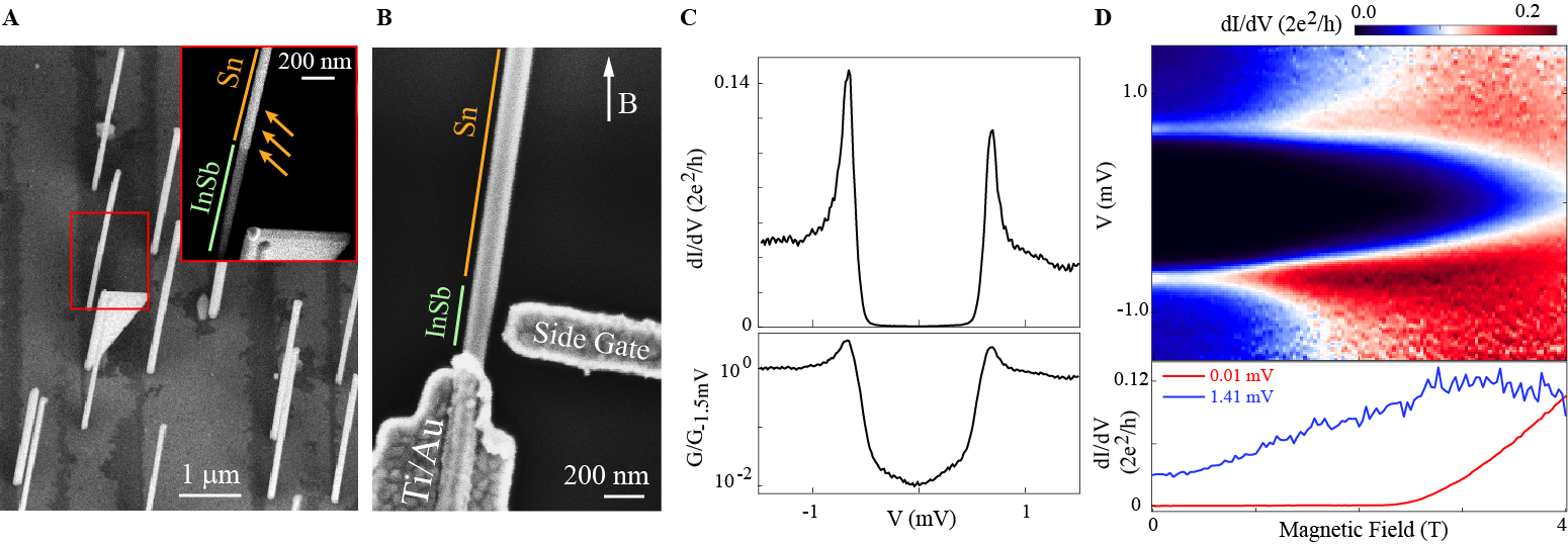
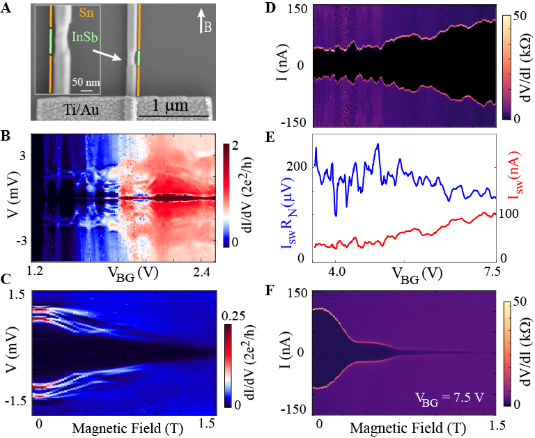
Our first goal is to investigate electron tunneling into Sn through InSb in the normal metal-superconductor (N-S) configuration. For this we need a nanowire with only one end covered by tin. We use the uncovered end to define a tunneling barrier and an N-contact. In order to avoid damage to InSb that results from etching away part of the Sn shell, we employ in-situ nanoscale shadowing Gazibegovic et al. (2017); Carrad et al. (2019). In this case it is an InSb flake, standing in front of the nanowire, that shadows the bottom of the wire during deposition of Sn in ultra-high vacuum Gazibegovic et al. (2019) (Fig. 1A).
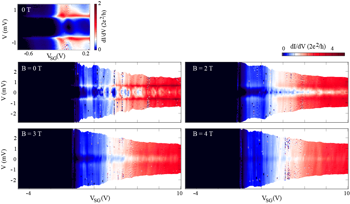
To prepare an N-S device the tin-coated nanowire is positioned onto a doped Si/ substrate which is used as a back gate (BG) (Fig. 1B). A side gate (SG) is used to define and tune the tunneling barrier near the edge of the tin-free segment. The tunneling spectrum reveals a two-orders-of-magnitude suppression in conductance around zero bias (Fig. 1C). This so-called hard gap indicates the elimination of decoherence pathways due to disorder and spurious subgap states. A superconducting tunneling peak is at eV which is comparable to the gap of tin. In magnetic field, the hard gap is found to persist beyond 2 Tesla, with the gap “softening” at higher fields and fully closing around 4 Tesla (Fig. 1D). Magnetic field resilience is an indicator of a thin uniform shell. It is another advantage of Sn since topological, spin and some superconducting qubits operate at high magnetic fields. Supporting Materials contain extended data images and source files for this device, for all devices presented in the main text and from additional devices.
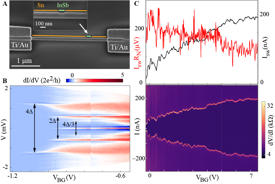
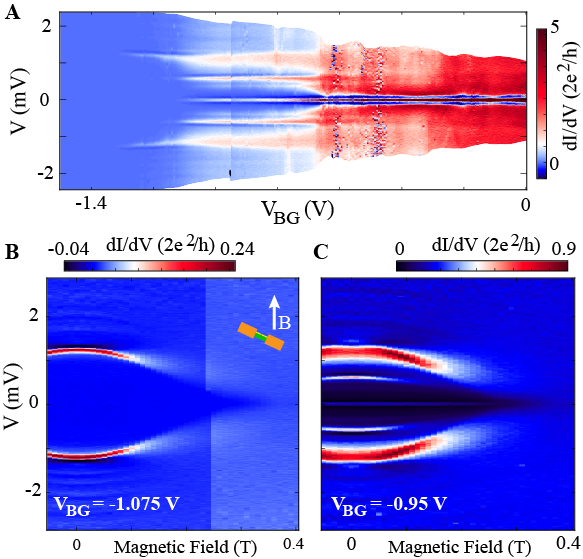
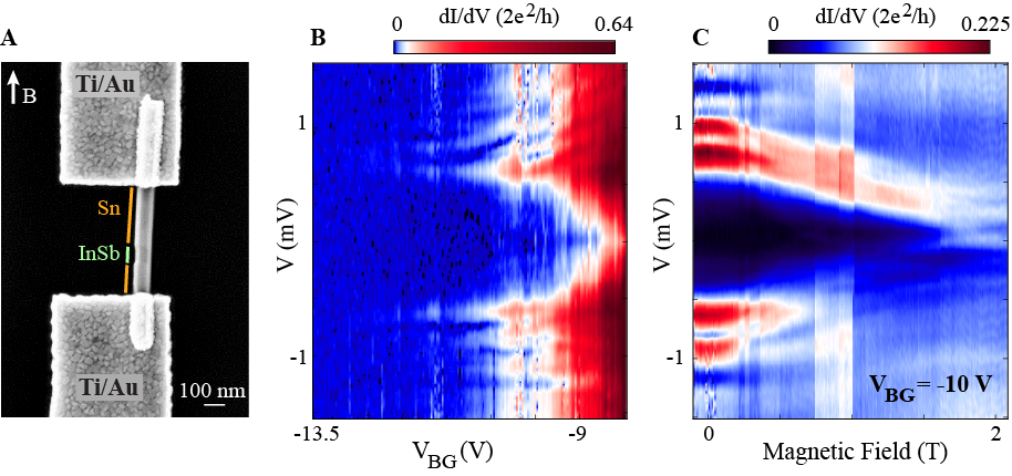
Next, we study superconductor-superconductor (S-S) devices with both ends of the nanowire covered by tin, and only a narrow break in the shell to define an InSb weak link (Fig. 2A). For this we use a previously developed method of shadowing the Sn flux by criss-crossing nanowires Gazibegovic et al. (2017). We first study tunneling between two tin islands (Fig. 2B). We observe a smooth nanowire pinch off void of accidental quantum dot states. Three finite-bias resonances are observed, marked 4, 4/2 and 4/3 in Fig. 2B. This sequence is a manifestation of Multiple Andreev Reflection processes, which are characteristic of transparent S-S junctions. They correspond to 615 eV 10 eV which is somewhat smaller than the gap observed in the N-S device (Fig. 1C). At V V only the 4 resonance is observed. We interpret this as the superconducting tunneling regime. Because the S-S tunneling resonance is a peak in current, it appears as a peak-dip structure in conductance.
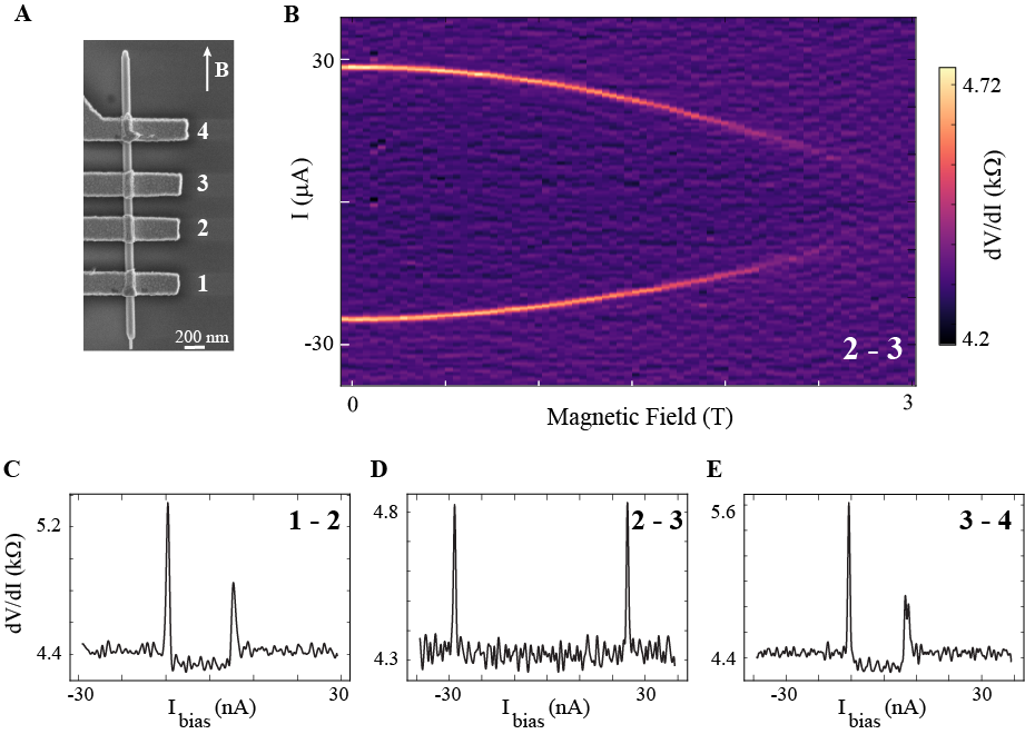
The resonance at zero bias in Fig. 2B is the Josephson supercurrent. This effect is best studied in the current-bias configuration (Fig. 2C). The switching current (I) from superconducting to normal state is a peak in differential resistance. I decays smoothly with more negative V. The current-voltage characteristics are weakly hysteretic which is reflected in the asymmetry of I in positive and negative current bias. In magnetic field, the Josephson effect is observed up to 1.5 T and remains significant with sharp switching up to 0.5 T (see Supporting Materials). This significant field range is a positive development for schemes that require coupling and decoupling of topologically superconducting islands at finite magnetic field for Majorana fusion or braiding Van Heck et al. (2012); Aasen et al. (2016). Measurements on continuous-shell nanowires without shadow junctions yielded supercurrents in the range A corresponding to the critical current density of A/cm2 (data in Supporting Materials). The extracted products IR (R is the normal state resistance) are in the range eV, which is significant, and of the same order of magnitude as the gap.
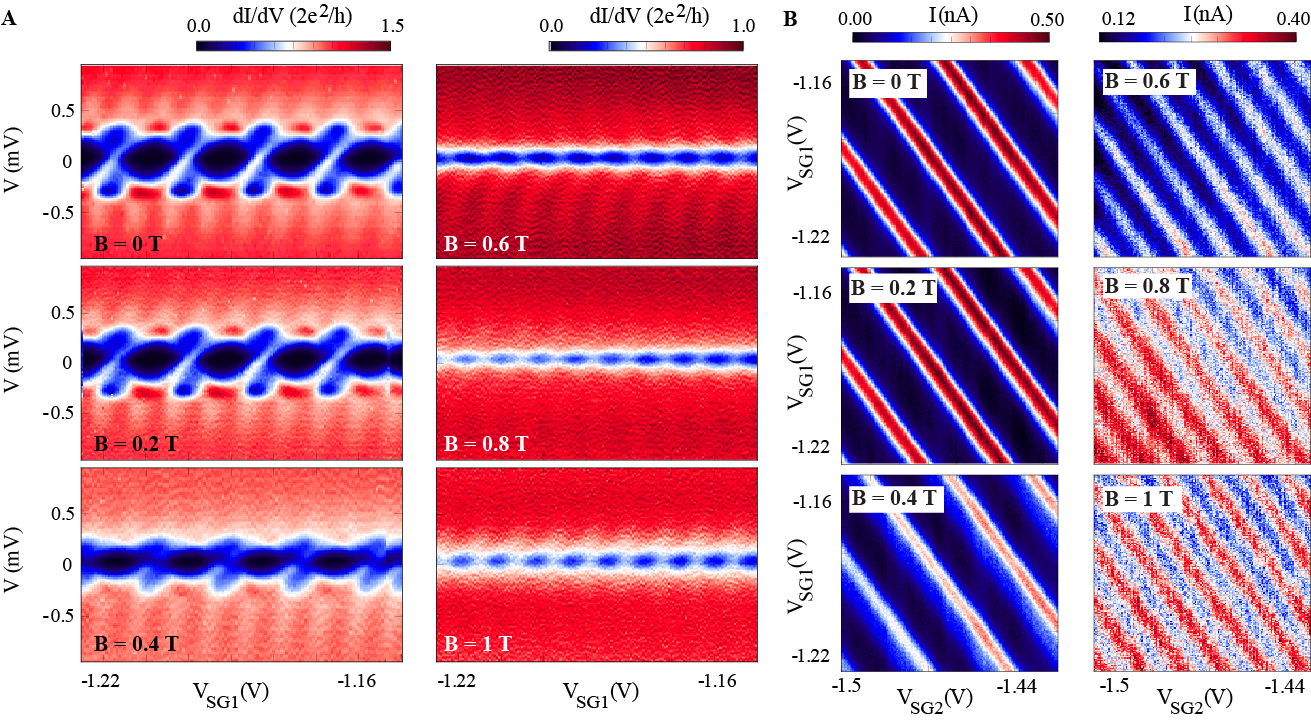
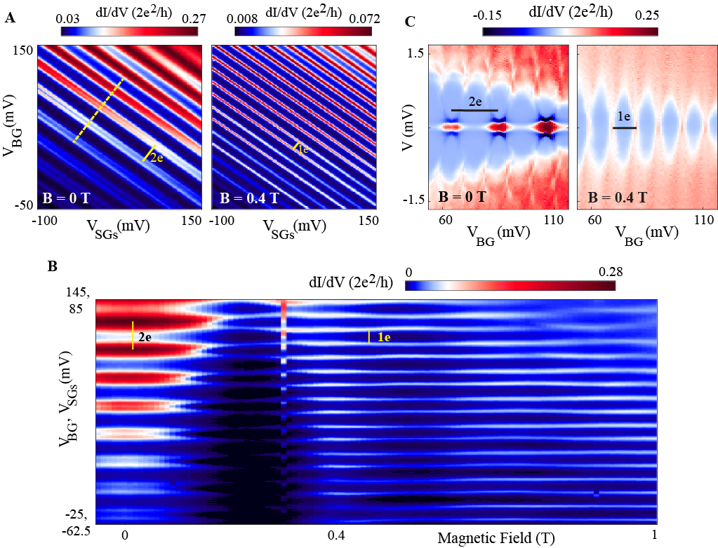
In Fig. 3 we present key findings on 2e charging of a tin island. The island is defined between two nanowire-shadow junctions in the N-S-N geometry (Fig. 3A). At zero magnetic field, we observe a single family of Coulomb peak resonances consistent with charging the entire island (Fig. 3B). At a finite magnetic field of 1 T, the frequency of Coulomb resonances doubles (Fig. 3C, 3D). We attribute data at zero field to 2e charging, and data at finite field to 1e charging. The transition from 2e to 1e is due to the superconducting gap or the lowest subgap state dropping in energy below the charging energy, which we estimate to be 0.3 meV (Figs. 3E, 3F). At finite magnetic field, it costs less energy to add electrons to the island one-by-one, while near zero field, due to hard gap superconductivity, it is advantageous to add electrons in pairs.
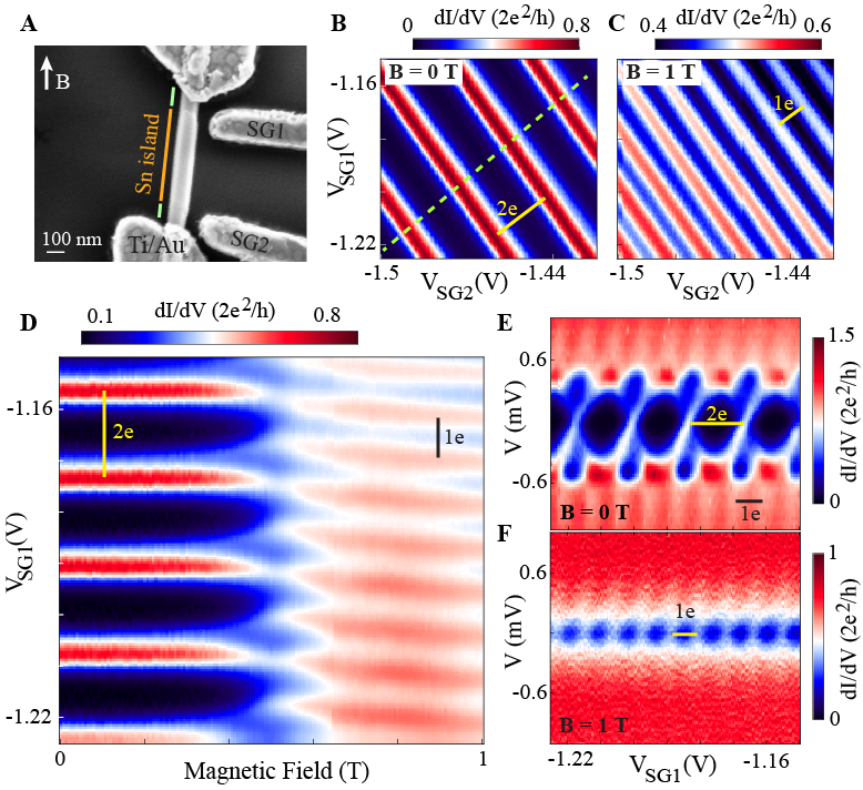
The two-electron charging effect is central for topological quantum computing because the states of a topological qubit are distinguished by even/odd island charge parity. If only 1e charging periodicity were observed, it would mean that despite a well-defined superconducting gap, electrons can be added to an island one at a time and the ability to distinguish the states of a topological qubit is scrambled. 1e periodicity is also detrimental for transmon qubits where single electron tunneling is a decoherence mechanism Serniak et al. (2018).
Tin is an unusual material which has two different crystal phases with a phase transition at 13C. The low-temperature -Sn has a diamond cubic lattice, while the high temperature -Sn is tetragonal. The electronic properties of both phases are very different. -Sn is a semimetal which can also be a topological insulator in monolayer form Xu et al. (2013, 2017); Zheng et al. (2019), whereas -Sn is a metal with a superconducting transition temperature of 3.7 K.
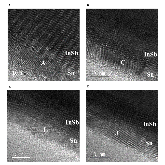
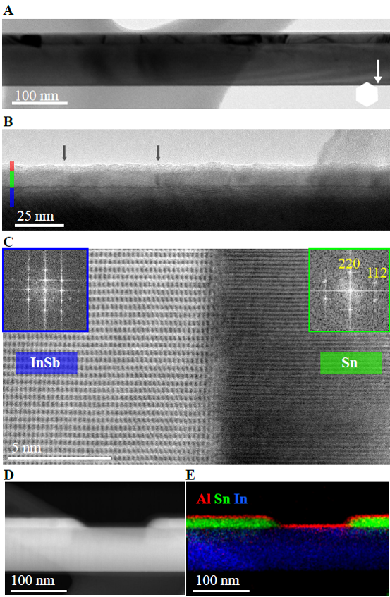
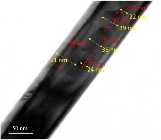
For tin on InSb nanowires we assess the structural properties and elemental distribution using transmission electron microscopy (TEM). TEM images reveal a polycrystalline Sn shell of uniform thickness around the InSb nanowire (Fig. 4A): the shell features grains of sizes nm to nm (see Supporting Materials). The Sn-InSb interface is abrupt and some Sn grains show epitaxial relationship with InSb. The high-resolution annular bright field-scanning TEM image (Fig. 4C) shows a section of the interface where the 111 planes of zincblende InSb are aligned with lattice planes of a Sn grain with a lattice distance of 2.04 Å. This matches the 220 interplanar distance of -Sn. This grain is one of 13 analyzed along the same nanowire. 11 of the grains are identified as -Sn from the fast Fourier transform analysis of the interplanar distances (Fig. 4C, inset). Only two of those -Sn grains show a preferential epitaxial relationship with InSb. In contrast, -Sn is lattice matched to InSb and can grow epitaxially Farrow et al. (1981). The predominantly -Sn shell observed at room temperature by TEM is in agreement with superconductivity observed at low temperatures, suggesting that no phase transformation of Sn occurred upon device cooldown.
In addition to the uniform shell thickness, the nanowire shadow junctions used in S-S and N-S-N devices are sharp with Sn islands defined abruptly on each side of the junction (Fig. 4C). Energy-dispersive x-ray spectroscopy (EDX) confirms that the Sn islands are isolated from each other and no interdiffusion between Sn and In is detected (Fig. 4D). A uniform 3-nm-thick passivation layer covers the entire nanowire. Oxidation at the Sn-InSb interfaces is not detected but cannot be fully excluded (see Methods).
Our results illustrate that neither defect-free epitaxial wire-shell interfaces nor single vacuum cycle growth of nanowire and shell are crucial requirements for the demonstration of hard gap, field-resilient superconductivity and 2e charging. We conclude and discuss in the Methods section that the key components in attaining robust induced superconductivity are (1) removal of InSb native oxide using atomic hydrogen prior to Sn growth, followed by (2) liquid nitrogen cooling of the nanowires during metal evaporation to produce a homogeneous ultrathin shell and (3) immediate passivation of the wire-shell hybrid with a stable dielectric.
We anticipate follow-ups of this work to be further research into the formation of Sn and InSb interfaces, and experiments in the Majorana geometry in search for robust signatures of topological superconductivity. Going forward, Sn/InSb nanowire system can be studied for applications in transmon and topological qubits. Beyond Sn, other metals can be tried as replacements of Al in search for decoherence free qubit materials Carrad et al. (2019); Bjergfelt et al. (2019); Güsken et al. (2017). Interface requirements may increase for full topological qubit devices for which the dominant decoherence mechanisms are yet to be established experimentally.
Methods
Nanowire growth. InSb nanowires are grown using the vapor-liquid-solid technique in a horizontal metal-organic vapor phase epitaxy reactor. The first nanowires used in this work are stemless InSb nanowires with flakes as shadow objects (Fig. 1A) Badawy et al. (2019); Gazibegovic et al. (2019). Both InSb nanowires and flakes are grown on an InSb (111)B substrate with a selective-area mask and gold as catalyst. The second type of nanowires, shown in Figs. 2A and 3B are shadowed by other nanowires Gazibegovic et al. (2017). The InP (100) substrates are etched to expose the two 111B facets, on which gold particles are deposited with an offset on the two opposing facets of a trench. Nanowires grow towards each other, such that the front wire shadows the back wire. InSb wires are grown on InP stems.
Sn shell growth. After transit in air, nanowire chips as grown are loaded into vacuum for subsequent growth of Sn shells. The chips are gallium bonded to molybdenum blocks. Atomic hydrogen cleaning is performed at 380C (thermocouple temperature) for 30 minutes, at an operating pressure of Torr consisting primarily of hydrogen ambient. Once cleaned, the samples are transferred in-vacuo to an ultra-high vacuum chamber dedicated for metal evaporation (base pressure Torr). Here, the nanowire samples are cooled to 85 K (-188∘C) for 2 hours, prior to tin evaporation. 15-nm-thick tin is then evaporated from an effusion cell at a growth rate of 7.5 nm/hr and an evaporation angle close to 60∘ from sample normal. This shallow evaporation angle aids in-situ formation of Sn islands with nanowire or flake shadows. After Sn evaporation, while the sample is still expected to be at cryogenic temperatures (due to the thermal mass of the molybdenum block), a 3-nm-thick shell of is electron-beam evaporated onto the nanowire sample, at normal incidence. The samples are then allowed to warm up to room temperature in vacuum.
Device fabrication and measurements. Device fabrication is similar to previous work on wires with epitaxial Al film Gazibegovic et al. (2017). Wires are transferred onto doped and thermally oxidized Si substrates using a micromanipulator under an optical microscope. Contacts and gates are patterned by electron-beam lithography by curing the resist at room temperature in vacuum to avoid nanowire heating and potential interdiffusion of Sn and In. Ar ion milling is performed to remove the layer before evaporating 10/150 nm of Ti/Au. Measurements are performed in a dilution refrigerator with a 30 mK base temperature using a combination of direct current and lock-in techniques. All voltage bias data are two-terminal measurements. A series resistance of due to measurement setup was taken into account in calculating conductance in all figures as well as renormalizing axis in Figs 2B, S1, S2A. TEM studies were performed using a probe corrected microscope operated at 200 kV, equipped with a 100 mm2 EDS detector.
Acknowledgements. Work supported by NSF PIRE-1743717, ANR HYBRID (ANR-17-PIRE-0001) and the Thomas Jefferson Fund. Solliance and the Dutch province of Noord Brabant are acknowledged for funding the TEM facility. CJP acknowledges Vannevar Bush Faculty Fellowship for characterization support at UCSB.
References
- Arute et al. (2019) F. Arute, K. Arya, R. Babbush, D. Bacon, J. C. Bardin, R. Barends, R. Biswas, S. Boixo, F. G. S. L. Brandao, D. A. Buell, et al., Nature 574, 505 (2019).
- Figgatt et al. (2019) C. Figgatt, A. Ostrander, N. M. Linke, K. A. Landsman, D. Zhu, D. Maslov, and C. Monroe, Nature 572, 368 (2019).
- Krantz et al. (2019) P. Krantz, M. Kjaergaard, F. Yan, T. P. Orlando, S. Gustavsson, and W. D. Oliver, Applied Physics Reviews 6, 021318 (2019).
- Kloeffel and Loss (2013) C. Kloeffel and D. Loss, Annu. Rev. Condens. Matter Phys. 4, 51 (2013).
- Lutchyn et al. (2018) R. Lutchyn, E. Bakkers, L. P. Kouwenhoven, P. Krogstrup, C. Marcus, and Y. Oreg, Nature Reviews Materials 3, 52 (2018).
- Hyart et al. (2013) T. Hyart, B. van Heck, I. C. Fulga, M. Burrello, A. R. Akhmerov, and C. W. J. Beenakker, Phys. Rev. B 88, 035121 (2013).
- Karzig et al. (2017) T. Karzig, C. Knapp, R. M. Lutchyn, P. Bonderson, M. B. Hastings, C. Nayak, J. Alicea, K. Flensberg, S. Plugge, Y. Oreg, C. M. Marcus, and M. H. Freedman, Phys. Rev. B 95, 235305 (2017).
- Plugge et al. (2017) S. Plugge, A. Rasmussen, R. Egger, and K. Flensberg, New Journal of Physics 19, 012001 (2017).
- Stenger et al. (2019) J. P. Stenger, M. Hatridge, S. M. Frolov, and D. Pekker, Physical Review B 99, 035307 (2019).
- Krogstrup et al. (2015) P. Krogstrup, N. L. B. Ziino, W. Chang, S. M. Albrecht, M. H. Madsen, E. Johnson, J. Nygård, C. M. Marcus, and T. S. Jespersen, Nature Materials 14, 400 (2015).
- Shabani et al. (2016) J. Shabani, M. Kjaergaard, H. J. Suominen, Y. Kim, F. Nichele, K. Pakrouski, T. Stankevic, R. M. Lutchyn, P. Krogstrup, R. Feidenhans’l, et al., Phys. Rev. B 93, 155402 (2016).
- Gazibegovic et al. (2017) S. Gazibegovic, D. Car, H. Zhang, S. C. Balk, J. A. Logan, M. W. de Moor, M. C. Cassidy, R. Schmits, et al., Nature 548, 434 (2017).
- Fornieri et al. (2019) A. Fornieri, A. M. Whiticar, F. Setiawan, E. Portolés, A. C. Drachmann, A. Keselman, S. Gronin, C. Thomas, T. Wang, R. Kallaher, et al., Nature 569, 89 (2019).
- Chang et al. (2015) W. Chang, S. M. Albrecht, T. S. Jespersen, F. Kuemmeth, P. Krogstrup, J. Nygård, and C. M. Marcus, Nat Nano 10, 232 (2015).
- Gül et al. (2017) O. Gül, H. Zhang, F. K. de Vries, J. van Veen, K. Zuo, V. Mourik, S. Conesa-Boj, M. P. Nowak, D. J. van Woerkom, M. Quintero-Pérez, et al., Nano Letters 17, 2690 (2017).
- Geerligs et al. (1990) L. J. Geerligs, V. F. Anderegg, J. Romijn, and J. E. Mooij, Phys. Rev. Lett. 65, 377 (1990).
- Tuominen et al. (1992) M. T. Tuominen, J. M. Hergenrother, T. S. Tighe, and M. Tinkham, Phys. Rev. Lett. 69, 1997 (1992).
- Lafarge et al. (1993) P. Lafarge, P. Joyez, D. Esteve, C. Urbina, and M. H. Devoret, Phys. Rev. Lett. 70, 994 (1993).
- Eiles et al. (1993) T. M. Eiles, J. M. Martinis, and M. H. Devoret, Phys. Rev. Lett. 70, 1862 (1993).
- Albrecht et al. (2016) S. M. Albrecht, A. P. Higginbotham, M. Madsen, F. Kuemmeth, T. S. Jespersen, J. Nygård, P. Krogstrup, and C. M. Marcus, Nature 531, 206 (2016).
- Shen et al. (2018) J. Shen, S. Heedt, F. Borsoi, B. van Heck, S. Gazibegovic, R. L. M. Op het Veld, D. Car, J. A. Logan, M. Pendharkar, S. J. J. Ramakers, et al., Nature Communications 9, 4801 (2018).
- Carrad et al. (2019) D. J. Carrad, M. Bjergfelt, T. Kanne, M. Aagesen, F. Krizek, E. M. Fiordaliso, E. Johnson, J. Nygård, and T. S. Jespersen, preprint arXiv:1911.00460 (2019).
- Pan and Sarma (2019) H. Pan and S. D. Sarma, preprint arXiv:1910.11413 (2019).
- Badawy et al. (2019) G. Badawy, S. Gazibegovic, F. Borsoi, S. Heedt, C.-A. Wang, S. Koelling, M. A. Verheijen, L. P. Kouwenhoven, and E. P. A. M. Bakkers, Nano Lett. 19, 3575 (2019).
- Plissard et al. (2012) S. R. Plissard, D. R. Slapak, M. A. Verheijen, M. Hocevar, G. W. G. Immink, I. van Weperen, S. Nadj-Perge, S. M. Frolov, L. P. Kouwenhoven, and E. P. A. M. Bakkers, Nano Letters 12, 1794 (2012).
- Nadj-Perge et al. (2012) S. Nadj-Perge, V. S. Pribiag, J. W. G. van den Berg, K. Zuo, S. R. Plissard, E. P. A. M. Bakkers, S. M. Frolov, and L. P. Kouwenhoven, Phys. Rev. Lett. 108, 166801 (2012).
- Nilsson et al. (2009) H. A. Nilsson, P. Caroff, C. Thelander, M. Larsson, J. B. Wagner, L.-E. Wernersson, L. Samuelson, and H. Q. Xu, Nano Lett. 9, 3151 (2009).
- Lutchyn et al. (2010) R. M. Lutchyn, J. D. Sau, and S. Das Sarma, Phys. Rev. Lett. 105, 077001 (2010).
- Oreg et al. (2010) Y. Oreg, G. Refael, and F. von Oppen, Phys. Rev. Lett. 105, 177002 (2010).
- Mourik et al. (2012) V. Mourik, K. Zuo, S. M. Frolov, S. R. Plissard, E. P. A. M. Bakkers, and L. P. Kouwenhoven, Science 336, 1003 (2012).
- Deng et al. (2012) M. T. Deng, C. L. Yu, G. Y. Huang, M. Larsson, P. Caroff, and H. Q. Xu, Nano Letters 12, 6414 (2012).
- Chen et al. (2017) J. Chen, P. Yu, J. Stenger, M. Hocevar, D. Car, S. R. Plissard, E. P. A. M. Bakkers, T. D. Stanescu, and S. M. Frolov, Sci. Adv. 3, e1701476 (2017).
- Gül et al. (2018) Ö. Gül, H. Zhang, J. D. Bommer, M. W. de Moor, D. Car, S. R. Plissard, E. P. Bakkers, A. Geresdi, K. Watanabe, T. Taniguchi, et al., Nature nanotechnology 13, 192 (2018).
- Zhang et al. (2018) H. Zhang, C.-X. Liu, S. Gazibegovic, D. Xu, J. A. Logan, G. Wang, N. van Loo, J. D. Bommer, M. W. de Moor, D. Car, et al., Nature 556, 74 (2018).
- Gazibegovic et al. (2019) S. Gazibegovic, G. Badawy, T. L. Buckers, P. Leubner, J. Shen, F. K. de Vries, S. Koelling, L. P. Kouwenhoven, M. A. Verheijen, and E. P. Bakkers, Advanced Materials 31, 1808181 (2019).
- Van Heck et al. (2012) B. Van Heck, A. Akhmerov, F. Hassler, M. Burrello, and C. Beenakker, New Journal of Physics 14, 035019 (2012).
- Aasen et al. (2016) D. Aasen, M. Hell, R. V. Mishmash, A. Higginbotham, J. Danon, M. Leijnse, T. S. Jespersen, J. A. Folk, C. M. Marcus, K. Flensberg, and J. Alicea, Phys. Rev. X 6, 031016 (2016).
- Serniak et al. (2018) K. Serniak, M. Hays, G. de Lange, S. Diamond, S. Shankar, L. D. Burkhart, L. Frunzio, M. Houzet, and M. H. Devoret, Phys. Rev. Lett. 121, 157701 (2018).
- Xu et al. (2013) Y. Xu, B. Yan, H.-J. Zhang, J. Wang, G. Xu, P. Tang, W. Duan, and S.-C. Zhang, Phys. Rev. Lett. 111, 136804 (2013).
- Xu et al. (2017) C.-Z. Xu, Y.-H. Chan, Y. Chen, P. Chen, X. Wang, C. Dejoie, M.-H. Wong, J. A. Hlevyack, H. Ryu, H.-Y. Kee, et al., Phys. Rev. Lett. 118, 146402 (2017).
- Zheng et al. (2019) X. Zheng, J.-F. Zhang, B. Tong, and R.-R. Du, 2D Materials 7, 011001 (2019).
- Farrow et al. (1981) R. Farrow, D. Robertson, G. Williams, A. Cullis, G. Jones, I. Young, and P. Dennis, Journal of Crystal Growth 54, 507 (1981).
- Bjergfelt et al. (2019) M. Bjergfelt, D. J. Carrad, T. Kanne, M. Aagesen, E. M. Fiordaliso, E. Johnson, B. Shojaei, C. J. Palmstrøm, P. Krogstrup, T. S. Jespersen, et al., Nanotechnology 30, 294005 (2019).
- Güsken et al. (2017) N. A. Güsken, T. Rieger, P. Zellekens, B. Bennemann, E. Neumann, M. I. Lepsa, T. Schäpers, and D. Grützmacher, Nanoscale 9, 16735 (2017).
- Su et al. (2018) Z. Su, A. Zarassi, J.-F. Hsu, P. San-Jose, E. Prada, R. Aguado, E. J. H. Lee, S. Gazibegovic, R. L. M. Op het Veld, D. Car, et al., Phys. Rev. Lett. 121, 127705 (2018).
- Zuo et al. (2017) K. Zuo, V. Mourik, D. B. Szombati, B. Nijholt, D. J. van Woerkom, A. Geresdi, J. Chen, V. P. Ostroukh, A. R. Akhmerov, S. R. Plissard, et al., Phys. Rev. Lett. 119, 187704 (2017).
- van Veen et al. (2018) J. van Veen, A. Proutski, T. Karzig, D. I. Pikulin, R. M. Lutchyn, J. Nygård, P. Krogstrup, A. Geresdi, L. P. Kouwenhoven, and J. D. Watson, Phys. Rev. B 98, 174502 (2018).
Supporting Materials
| Grain | (exp) | hkl | (lit) | % deviation from lit | hkl | (lit) | % deviation from lit | epitaxy |
|---|---|---|---|---|---|---|---|---|
| A | 0.198 | 211 | 0.2010 | -1.2% | 311 | 0.1956 | +1.5% | |
| C | 0.209 | 220 | 0.2065 | +1.0% | 311 | 0.1956 | +6.7% | YES |
| D | 0.203 | 220 | 0.2065 | -1.4% | 311 | 0.1956 | +4.1% | |
| 211 | 0.2010 | +1.3% | - | - | - | |||
| E | 0.206 | 220 | 0.2065 | -0.4% | 311 | 0.1956 | +5.1% | |
| F | 0.205 | 220 | 0.2065 | -0.5% | 311 | 0.1956 | +5.0% | |
| G | 0.274 | 101 | 0.2772 | -1.3% | 211 | 0.264 | +3.7% | |
| I | 0.282 | 101 | 0.2772 | +1.7% | 211 | 0.264 | +6.7% | |
| J | 0.277 | 101 | 0.2772 | -0.0% | 211 | 0.264 | +5.0% | |
| K | 0.203 | 220 | 0.2065 | -1.8% | 311 | 0.1956 | +3.7% | |
| L | 0.267 | 101 | 0.2772 | -3.7% | 211 | 0.264 | +1.1% | |
| M | 0.280 | 101 | 0.2772 | +1.2% | 211 | 0.264 | +6.2% | |
| N | 0.287 | 200 | 0.2920 | -0.8% | - | - | - | |
| R | 0.204 | 220 | 0.2065 | -1.2% | - | - | - | |
| 0.149 | 112 | 0.1472 | +1.3% | - | - | - |
Table S1. Phase identification based on lattice spacings dhkl of 13 Sn grains imaged using high resolution TEM. All dhkl values are determined from Fast Fourier Transform patterns constructed from the HRTEM images. All patterns were calibrated by InSb lattice spacings present in the same images. The 211 spacing is not allowed based on crystal symmetry, but can appear in HRTEM images. The experimental inaccuracy in the dhkl values is estimated to be 2.0 percent considering the limited number of pixels in the FFT patterns. Based on this criterion, apart from grains A and L all grains can be assigned to the -Sn phase. Grain R is presented in Fig. 4C.
