Crystallographic Characterization of Black Phosphorene and Its Application in Nanostructures
Abstract
The central question in the field of two-dimensional (2D) materials is how a material behaves when it is patterned at nanometer scale with different edge geometries. Due to the anisotropy inherent in the puckered structure, black phosphorene nanostructures may have more varieties of edge geometries. Here, we present a comprehensive 2D planar crystallographic characterization of phosphorene uniformly by a chiral vector (angle), from which a new type of edge atomic configuration, the slope edge geometry is discovered. The phosphorene nanoribbons (PNRs) with slope edges, like previously noticed zigzag and skewed-armchair PNRs, also own interesting twofold-degenerate edge states. These three marginal directions, together with the skewed-zigzag and armchair directions without edge states, divide a phosphorene into four regions among which the electronic property is different from each other. Further, for a PNR cutting along any possible direction, by taking into account the -direction in structure, whether or not it owns edge states depends on the existence of periodic zigzag-like morphology along the edges. For application, moreover, we propose a PNR-based z-shaped homogenous junction with scale 100 nm, where the central scattering region between two PNR electrodes is a phosphorene quantum dot (PQD) of PNR segment with various edge morphologies. Interestingly, the calculated conductance by Kwant code based on tight-binding combing with scattering-matrix for the junction relies sensitively on the central PQD edge states. In specification, for the junctions of PQD with edge states the conductance exhibit a terrace with resonant oscillations near Fermi energy, otherwise the electron transport is blocked due to the absence of edge states. Remarkably, the number of oscillating peaks exactly matches to the number of sawtooth along an edge of PQD, since the discrete energy levels of the zigzag-like edge provide the transporting channels for electrons. The results here may be extended to the group-VA 2D materials for observing the electronic property of nanostructures in experiments, and provide a reference for the preparation of better nano-devices.
pacs:
73.22.-f, 73.63.-b, 68.65.-kI Introduction
In this decade, two-dimensional (2D) materials have emerged as one of the most exciting class of materials since the arising of graphene Geim . Recently, semiconducting black phosphorous (or phosphorene), a mono- or few-layer of phosphorus atoms forming 2D puckered sheets, has joined the class of 2D materials Li ; LiuH ; XiaF ; Steven ; Buscema ; Ling . The synthesized phosphorene has a noticeable band gap and appreciable anisotropy in its physical properties Ling ; Rishabh ; Chen . Generally, a 2D material may display the properties differing greatly from its bulk counterpart due to the effects of quantum confinement and large surface-to-volume ratio. Further, tailoring a 2D material along its different crystallographic directions can obtain one-dimensional (1D) nanoribbons with the width less than 100 nm Tao ; LiY ; Mitchell ; Carvalho ; Marko . These nanoribbons show not only the confinement effect but also peculiar edge effect, both of which play an important role in electronic, optical, magnetic and transport properties SGLouie ; Tran ; Ajanta ; YangG . Hence the edge states are particularly important in a 2D material nanoribbon.
Black phosphorus, with an anisotropic structure, is a van der Waals-bonded layered material where each layer forms a puckered surface due to sp3 hybridization and possesses a direct band gap of 0.3 eV HanCQ . This direct gap increases up to 2 eV as its thickness decreases from bulk to few layers Li1 . In addition, the field-effect transistor (FET) Li ; Steven ; Buscema based on phosphorene is found to have an on/off ratio of and a high hole carrier mobility up to 800 cm2/Vs Sherman . Importantly, there have been a few effective ways to solve the instability problem for phosphorene in the environment Niu . These good properties of phosphorene have attracted a broad interests Zhou ; Zhou1 ; Li2 ; Quhe ; Gautam . Further, PNRs by tailoring a phosphorene sheet in the conventional zigzag and armchair directions have been prepared experimentally Paul ; Mitchell , respectively. The zigzag PNRs (ZPNRs) with significant edge states and armchair PNRs (APNRs) with direct band-gap have been extensively studied Carvalho ; Tran ; Ezawa ; Ajanta . And some properties of PNRs have been verified YangG ; Esmaeil ; Sousa ; SK ; Ren ; Sisakht ; ZhouBL ; Han , such as the effect of edge states on conductance and thermalpower Ma , the influence of vacancy defects on electron structure and transport Zahra ; Lill , and the electric tunable edge-pseudospin valve Soleimanikahnoj .
On the other hand, the nanostructures with various possible edge atomic configurations have become a hot topic since the rise of 2D materials. A central question in the field of graphene-related research is how it behaves as patterned at the nano-scale with different edge morphological geometry Tao ; Akhmerov . If we cut a graphene sheet along crystal directions by increasing the chiral angle from 0∘ to 30∘, for example, the edge geometry switches from zigzag to armchair, between which we can obtain all possible chiral ribbons with different chiral angles Tao ; Akhmerov . Recently, the effects of chirality and edge geometry on the anisotropic thermal transport property have also been studied for MoS2 nanoribbons LiuT . For PNRs, in addition to the conventional zigzag and armchair edges, other edge geometries have been predicted. For example, the PNRs with stable edges of beard-zigzag Ezawa , skewed-zigzag (SZ) and skewed-armchair (SA) Marko ; Ashwin ; Liu have also been reported. And some of them have already been realized experimentally Liang . The electronic property, essentially, is significantly different from each other among PNRs with different chiralities. This difference results in abundant electrical nature, such as metal with edge states and semiconductor with direct band gap. Furthermore, the difference in physical properties has potential applications. For instance, the control of external electric and magnetic fields on the electronic structure Vladimir and the coupling and manipulation of the edge states in multilayer PNRs Lv . However, the existed studies have only involved PNRs with above mentioned few particular edge geometries. An uniform verification of the edge morphology for highly anisotropic phosphorene, as those for isotropic graphene Tao ; Akhmerov , is also important in the phosphorene-based nanotechnology.
In this work, we first present theoretically the 2D planar crystallographic characterization on an anisotropic phosphorene. We define a chiral number (vector) or chiral (azimuthal) angle to uniformly describe the planar crystallographic directions. As the chiral angle increasing from 0 to 90 shown in Fig. 1, the boundary morphology switches from zigzag to armchair and sweep over all possible edge geometries during the process. We find a phosphorene can be divided into four fan-shaped regions determined by chiral angles 0, , , and 90, among which the electronic characteristics is different. Therefore, by cutting a phosphorene along these five regional boundary directions, one can obtain previously studied ZPNR, SAPNR, SZPNR, and APNR Marko ; Ashwin ; Liu . Importantly, the PNR with sloped (SL) edge geometry along (named as SLPNR) between SZ and armchair direction has not been reported yet. Essentially, the SL direction is similar to SA with a periodic zigzag-like edge morphology supporting edge states. Further, by taking into account the effect of the -direction in structure, we then demonstrate the variation of electronic property for PNRs with different edge atomic geometries by the Kwant code based on tight-binding (TB) calculations Groth , in which a particular attention is paid to the new SLPNR intrinsically with twofold-degenerate edge states. In addition, the origin of beard and non-beard edges along each regional boundary direction is discussed and related to the existence of edge states. The result here may be extend to the cousins of phosphorene, such as 2D group-VA arsenene, antimonene and bismuthene ZhangSL .
Second, based on the 2D crystallographic characterization, we propose a two-terminal z-shaped homogenous junction based on PNR and calculate its transport property using the Kwant code based on TB Groth combined with scattering matrix approach from wavefunction-matching Yongjin ; Zwierzycki ; Tatiane for treating large enough systems comparable with experimental samples. The two electrodes of the junction are semi-infinitive ZPNRs with the same width 100 nm, where the central scattering region of a segment of PNR with edge tilting angles from 0 to 90 is sandwiched between them. In consequence the two hypotenuse edges of the central phosphorene quantum dot (PQD) sweep over all possible geometrical morphologies. Interestingly, the conductance spectrum sensitively depends on the tilting angle of -shaped junction. For the junctions of PQD with edge states the transport behavior exhibit a conductance terrace with resonant oscillation in the low energy regime, otherwise the electron transport is blocked due to the absence of edge states. Remarkably, the number of conductance oscillating peaks is exactly equal to the number of outermost phosphorus atoms in zigzag-like edges of the center PQD, since the discrete energy levels of the zigzag-like atomic configurations provide the transport channels for electrons. These findings may provide a reference for experimental preparation of better nano-devices.
This paper is organized as follows. Sec. II we first present the 2D crystallographic characterization of phosphorene, in which the crystallographic direction on the plane is uniformly described by a chiral vector or angle. By this vector (angle) the crystallographic directions with possible boundary edge geometries are identified, particularly including the newly recovered slope edge. Further, the calculation method by using the Kwant code based on tight-binding (TB) combing with scattering matrix approach is described. In Sec. III, firstly a few examples of typical PNRs with stable structure are analogized, and then the PNR-based z-shaped junction with different tilting degrees, in which the central PQD with various edge morphologies, is constructed, and the transport property is studied in details. And the main results are presented numerically with the microscopic explantation and discussion. Finally, we summarize our results in Sec. IV.
II Model Description and Method
II.1 2D crystallographic characterization
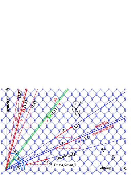
Phosphorene is a typical orthorhombic-structured 2D material with two principal crystallographic directions, the zigzag and armchair directions, as shown in Fig. 1, denoted as the -axis and -axis, respectively. It is known that the period of minimum rotation angle for graphene is 30∘ from zigzag to armchair direction Tao ; Akhmerov . Due to the highly anisotropic structure of phosphorene, however, it needs to anticlockwise rotate 90∘ from the zigzag to armchair direction. In consequence, there may exist more possible directions along which form PNRs by cutting a phosphorene in addition to along the conventional zigzag and armchair directions, as well as the previously verified SA and SZ directions Marko ; Liu . Therefore, an unified identification for the crystallographic direction on 2D phosphorene is still in great demand.
The low symmetry of phosphorene leads to higher structural complexity compared to other 2D materials Tao ; Akhmerov ; LiuT , such as graphene, silicene, -BN, and MoS2 which all have a regular hexagonal symmetry in 2D. In the previous works, the symmetry of phosphorene has been studied in terms of the point group theory LiPK . In order to simply characterize the crystallographic directions for phosphorene by using the inversion symmetry to reduce the degree of freedom Ezawa ; LiPK , here we firstly ignore the -direction in structure and add its effect on nanostructures in the next step. This simplification means that there are only two atoms in a primitive cell instead of the standard four atoms per primitive cell. Therefore, the 2D planar crystallographic directions of a phosphorene can be characterized by an orientational (chiral) index , or equivalently, a chiral angle . Further, or also determines a minimum unit vector along the corresponding crystallographic direction. Therefore, we can define a chiral vector to characterize the crystallographic directions, which is given by
| (1) |
Here and are the primitive vectors of phosphorene, with amplitudes =3.32 and =4.38 along the - and -directions Rudenko , respectively. The module of is the hypotenuse length of the (red) dot-dashed line right-angled triangle for each direction shown in Fig. 1. Hence m and n are integers for the projection of onto - and -directions in terms of /2 and /2, respectively. In order to ensure both and are integers, the two sides of right-angled triangle in Fig. 1 are taken as half of the primitive vectors. Thus, we can obtain a series of possible crystallographic directions of phosphorene only when m+n=even because the m+n=odd case is unphysical according to our definition of . To satisfy the condition for the chiral index, both m and n must simultaneously be even or odd. As a result their difference is also an even integer. Particularly, =0 corresponds to chiral index =(1,1) for the SZ direction. In addition, when the difference is a nonzero even number, the corresponding chiral index is (3,1), (1, 3) and (5, 1), and so on, respectively (also see Fig. 1).
Meanwhile, we can accordingly introduce a chiral angle as
| (2) |
with which connects the chiral index . Therefore, a crystallographic direction on the phosphorene plane can be characterized by either a chiral vector or index , or angle . Despite all this, however, the structural characterization is still much different from that for graphene with a regular hexagonal symmetry Akhmerov .
| zigzag-SA | SA-SZ | SZ-SL | SL-armchair | |||||
|---|---|---|---|---|---|---|---|---|
| (2,0) 0 | (3,1) 23.74 | (1,1) 52.84 | (1,3) 75.82 | |||||
| (2+1,1)0 | (4,2) 33.41 | (,+2)52.84 | (1,5) 81.38 | |||||
| (5,1) 14.78 | (+2,)52.84 | (2,4) 69.24 | (1,2+1)90 | |||||
| (3,1) 23.74 | (1,1) 52.84 | (1,3) 75.82 | (0,2) 90 |
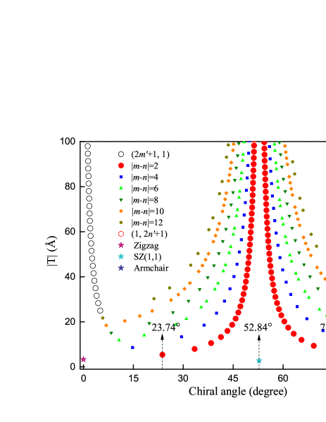
For specification, in Fig. 2 we present (the modulus of ) as a function of from 0 (zigzag) to 90 (armchair), where the different colored and shaped dots denote for the different combinations of m and n. For example, the (red) spheres indicate the value of for =2, the (blue) squares for =4, and so on. Importantly, the (black) and (red) circles denote the values for (2+1,1) and (1,2+1), which correspond to the directions with chiral angle near 0 and 90, respectively. As shown in Fig. 2, the distribution of varying with for the directions simultaneously obey =2, (2+1,1) and (1,2+1) forms an interesting pattern of two separated U-shapes. All other points with different chiral indexes are located inside the U-shapes, except for the three star-indicated special points. One is the (green) star-indicated split-point between two U-shapes at =52.84∘ (SZ direction), along which =. The other two (brown) and (blue) star points at =0∘ and 90∘ correspond to the two boundaries of zigzag and armchair, respectively. Further, the bottoms of two U-shapes are at the two special chiral angles of 23.74∘ and 75.82∘, respectively, which correspond to the SA and newly discovered SL directional boundaries. Moreover, with the increase of , become longer and and the atomic configuration of the corresponding boundary turn out to be more complicated.
Based on the above description we conclude that, as shown in Fig. 1 and Tab. I, a phosphorene can essentially be divided into four major regions as the chiral vector rotates around the -axis from the zigzag direction at chiral angle =0∘ to the armchair at 90∘. And these four regions are also indicated by the angle ranges of 0-, -, - and -90, with the regional boundaries determined by the five crystallographic directions along zigzag, SA [(blue) thick solid line], SZ [(green) thick solid], SL [(red) thick solid] and armchair, respectively. More specifically, the crystallographic directions of the reginal boundaries are described by indexes (2,0), (3,1), (1,1), (1,3) and (0,2) respectively at =0, , , and 90∘, or equivalently by the unitary vector length =, , , and . We notice that, excepting for the new SL, the other four peculiar directions and their corresponding PNRs have been previously studied Marko ; Ashwin ; Liu . The PNRs cutting along SL direction also with stable edges, however, has not been reported yet.
Further, there also exist other crystallographic directions within each region, which are exemplarily shown in Fig. 1 by the thin solid lines. Along these directions the projection of unitary vector on the horizontal (vertical) axis can be obtained by combination of /2 (/2). For instance, when the chiral angle rotates anticlockwise from with ()=(3,1), the vertical component of is always kept as /2 since the data are in the left periphery of the first ’U’ (see Fig. 2), and the horizontal one can be added with integer times of , such as (5,1) shown by the (blue) thin solid lines shown in Fig. 1. And the subsequent possible crystallographic directions in this region are listed in the first column of Tab. I. Similarly, when the chiral angle rotates anticlockwise from to (SA to SZ), the corresponding horizontal (vertical) component of varies in times of /2 (/2), such as (4,2). And a series of possible directions are also presented in the second column of Tab. I. However, according to the above derivation rule, we can not get the varying law for boundaries from SZ to the armchair direction. Therefore, to complete phase diagram, the new SL directional boundary must be filled in the region from SZ to the armchair. When the chiral angle rotates clockwise from to (SL to SZ), the horizontal (vertical) projection of varies with times of /2 (/2). In contrast, as the SL direction rotates anticlockwise to the armchair there is a change of multiple for the vertical component of but the horizontal one maintains unchanged due to the data for the boundaries are distributed in the right periphery of the second U. The resulting series of boundary chiral numbers are shown in the third and fourth columns in Tab. I, respectively. The examples of the crystal directions with chiral indexes (4,2), (2,4) and (1,5) from to 90 are indicted in Fig. 1 by the (blue) and (red) thin solid lines, respectively. However, as shown by the colored stars in Fig. 2, the data for the three special boundary directions, zigzag, SZ and armchair, are outside the U-shape valleys. In fact the nanostructures with these edges are most stable and favorably formed in experiments Liang .
Moreover, when we cut a 2D phosphorene sheet along a certain crystal direction, in fact, there exist two different manners for tangent to atoms due to the two nonequivalent phosphorus atoms per primitive cell. Therefore, the direction (1,1)52.84 is very particular, behind/beyond along which the boundary edge is non-beard/beard when tangent to the lower atom, and viceversa when tangent to the upper atom of the primitive cell. That is to say, SZ is the demarcation line between with and without beard for the boundary edges. Further, for cutting manner by the solid lines in Fig. 1, all the boundary edges have an obvious zigzag-like edge atomic morphology except along the SZ and armchair directions. Whether a boundary edge is bearded or non-beard depend on the number of dangled bonds of the outermost atoms. For beard/non-beard boundary edge, the number of dangled bonds of the outermost atoms is two/one per atom.
Actually, when we consider the phosphorene nanostructures the effect of the -direction on the characterization must be taken into account. This effect can be reflected by the fact that there are two kinds of arrangement for the outermost atoms along each crystallographic direction. According to our definition for , the chiral indexes satisfying m+n=even have defined the all directions for a phosphorene sheet shown in Fig. 1. When both m and n are odd, however, the outermost phosphorus atoms along the direction are alternately located at the upper and lower sublayers. So the supercell width of the nanoribbon cutting along this direction is twice as . The typical example of this case is shown by the (red) thick solid line segment along SA(3,1) direction in Fig. 1. In comparison, when both m and n are even, the outermost atoms are located at the same sublayer. In this case the supercell width is just [see the (4,2) direction]. The detailed classification on nanoribbons is discussed in the Supplemental Material SM .
II.2 PNRs and the PNR-based z-shaped junction
According to the structural characterization on phosphorene in the previous subsection, one can principally obtain PNRs with different edge morphologies by cutting a phosphorene sheet along different crystallographic directions. In addition to the extensively studied ZPNR and APNR Carvalho ; Ezawa , the ribbons by cutting along other three regional boundary directions SA(3,1), SZ(1,1) and SL(1,3), indicated by the thick solid lines in Fig. 1, are respectively denoted as (3,1)nbPNR, (1,1)bPNR and (1,3)bPNR, where bPNR or nbPNR means a ribbon with or without beard edges. On the other hand, when the ribbons by cutting along SA(3,1), SZ(1,1) and SL(1,3) according to the dashed lines in Fig. 1 are denoted as (3,1)bPNR, (1,1)nbPNR and (1,3)nbPNR, respectively. These six types of PNRs are respectively sketched in Figs. 3(a-f), where the (red) dashed parallelogram in each PNR indicates its minimum periodical supercell. Since their outermost atoms along these ribbon edges are alternately located at the upper and lower sublayers, their supercell width is twice as for both beard and nonbeard edges. Among these ribbons only (3,1)PNR and (1,1)PNR have been previously studied Marko . For (1,3)PNRs along SL, the chiral angle is 75.82∘ and the edge morphology is more likely to APNR, which is obviously different from (3,1)PNRs along SA (23.74∘) near zigzag edge. In addition, these ribbons obviously do not have the mirror symmetry as the normal ZPNR and APNR Carvalho . As mentioned in the above subsection, the ribbons cutting along SA and SL solid line have a periodic zigzag-like edge morphology. Importantly, this edge morphology are destroyed for the ribbons along the dashed line directions. Therefore, for reflecting the particular edge atomic morphology, as show in Figs. 3(a-f), we have to choose different (red) dash-line parallelograms as the supercells for (3,1)nbPNR, (1,1)bPNR, (1,3)bPNR, (3,1)bPNR, (1,1)nbPNR and (1,3)nbPNR, respectively.
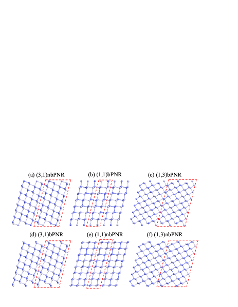
The stability of PNRs is an important issue which has been previously studied by calculating the free energy Han ; Ashwin . Since the stability for (3,1)PNR and (1,1)PNR has been studied in previous work which implies that the non-beard ribbon is more stable. So in this work, we just compare the stability of the three ribbons in the case of non-beard, and also study the difference in stability between (1,3)bPNR and (1,3)nbPNR. Using the first-principles calculation based on the density functional theory (DFT) Ren , we have verified the binding energies of the four narrow ribbons shown in Figs. 3(a, c, e, f). The order of the stability for these ribbons is (1,1)nbPNR, (3,1)nbPNR, (1,1)nbPNR, (1,3)nbPNR, (1,3)bPNR, with width 2 nm. With the increase of width, the ribbons will become more stable with lower binding energies.
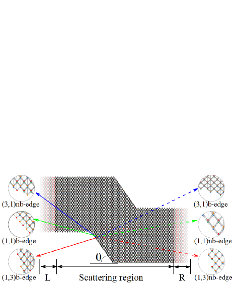
Next, we propose a two-terminal z-shaped junction based on PNRs as shown in Fig. 4, where the electrodes of the junction are two semi-infinitive ZPNRs with the same width 100 nm and the central scattering region is a z-shaped phosphorene quantum dot (PQD) which contain a segment of PNR with different tilting angles. The tilting angle of PQD corresponding to the chiral angle varies from 0 to 90∘, as a result the two hypotenuse edges of PQD sweep over all possible geometrical morphologies. The enlarged typical edge geometry of the ribbons in Figs. 3(a-c)/(d-f) are shown in the left/right side of Fig. 4. This type of homogeneous junctions may be etched on a sample sheet of 2D materials as the development of experimental technology, and it has been extensively studied for graphene, silicene, -BN, and so on Lee ; WangZF . However, for phosphorene the edge (state) effect has only been considered for quantum dot and ring structures ZhangR ; ZhangR1 , although the PNR-based z-shaped junction has been primarily studied Enrique . In this work, we further study this z-shaped PNR junction to explore the influence of the variation in edge geometrical morphology (corresponding to different tilting angle) on the transport property. The significance is that the connection between the different parts in homogeneous junction does not destroy the original lattice structure. This may be impossible for inhomogeneous heterojnuctions with another material electrodes because there is always a lattice mismatch. Furthermore, the z-shaped junction allows short ribbon with all possible edges embedded in the junction, in which the existence of resonant tunneling phenomenon Katsunori can be expected.
II.3 Computational details
The numerical calculations here are performed by using Kwant code based on the tight-binding (TB) Hamiltonian, and the atomistic quantum transport simulations are based on the scattering-matrix approach from solving wavefunction Yongjin ; Zwierzycki ; Tatiane . Compared with the conventional first-principles calculations Ren , this method can calculate large nanostructures matching the usual experimental reachable sample size up to sub-100 nm scales with better precision Groth . This advantage enables us to truly explore the electron structure and transport property for the phosphorene nanostructures with different edge morphologies realized in experiments, and to provide a fundamental understanding in preparation for the design of nano-devices Lill ; Anffany .
In specification, the ribbons shown in Fig. 3 and the junction shown in Fig. 4, in which the system with and without beard edges is respectively considered, and the stability is analyzed by the first-principles approach. In the calculation the scale of the systems is adapted about 10-30 nm to meet the current experimental development Anffany , which is large enough to show a good illustration of the credibility and feasibility for the calculated results. This scale is more suitable for using Kwant, a Python package for numerical quantum transport calculations. We use a TB model based on the quasi-particle orbit to describe the low-energy electrons in phosphorene Rudenko . The parameters of the TB model are obtained by fitting its low-energy band structure of phosphorene to the one computed by the DFT-GW approach Rudenko , and it was shown that the fitted TB model can reproduce well the band structure of phosphorene in the low-energy regime as compared to the DFT-GW approach Rudenko .
The formal TB Hamiltonian for the considered system is
| (3) |
where the summation runs over all lattice sites, is the on-site energy at site , is the hopping energy between sites and , and () is the creation (annihilation) operator of an electron at site (). It has been shown that five hopping parameters (see Fig. 1) are enough to describe the electronic band structure of phosphorene with hopping energies =-1.220 eV, =3.665 eV, =-0.205 eV, =-0.105 eV, and =-0.055 eV Rudenko . Starting from the Hamiltonian, we can calculate the local density of states (LDOS) using the following formula
| (4) |
where is broadening parameter, and are the eigenfunction and eigenvalue, respectively, in which denotes the energy band index and the atom position. Further, the conductance of the junction at zero temperature can be calculated by using the Landauer formula Datta
| (5) |
where = is the equilibrium distribution function with Fermi energy , L/R labels the left/right electrode of the system, and = is the transmission coefficient through the junction from electrode to , in which is the retarded (advanced) Green function of the central region, and the coupling matrix between the scattering region and the left/right electrode.
III Numerical Results and Discussions
III.1 Electronic structure for PNRs
By solving the difference Schrödinger equation corresponding to Hamiltonian on the proper basis for the supercell adopted in Fig. 3 and applying the Bloch theorem, the -dependent Hamiltonian for a PNR can be written as = in the form of () dimensional matrix. Here is the number of atoms in the supercell drawn by the (red) dashed line in Fig. 3, is the matrix of the central cell, the coupling matrix with the right-hand adjacent cell, and is the length between two nearest-neighbor cells. Diagonalizing this -dependent Hamiltonian, we can obtain the band spectrum and the corresponding eigen-wavefunctions. And following the procedure described in the last subsection, we can also obtain the conductance and LDOS for the system.
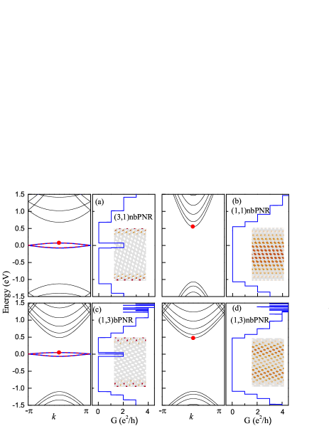
The calculated energy band (the left panel) and conductance (right panel) are shown in Figs. 5(a-d) for the four most stable (3,1)nbPNR, (1,1)nbPNR, (1,3)bPNR and (1,3)nbPNR with width around 4 nm, respectively. And the choice of the supercells has consequently taken the effect of the -direction into consideration. In each figure the embedded inset in the right panel is the LDOS at energy indicated by the (red) dot in the corresponding left panel. First, for the band structure of (3,1)nbPNR shown in Fig. 5(a), the twofold-degenerate edge bands indicated by the (red) dashed and (blue) solid lines pass through the Fermi level exhibiting metallic property, while (1,1)nbPNR is a direct band gap semiconductor as shown in Fig. 5(b). This recovers the results by previous straightforward calculation for these two types of ribbons Marko . However, for the newly discovered (1,3)bPNR the twofold-degenerate edge bands around the Fermi level are also detached from the bulk bands. This is similar to the band structure of (3,1)nbPNR, but the bulk band (black thin solid line) and its position relating to edge state are still significantly different. To further confirm the existence of the edge states, we have calculated the LDOS at the energy marked by the (red) dots on edge bands, the thumbnail of LDOS embedding in the right panels depicts the real-space localization of electrons. From the LDOS for (3,1)nbPNR and (1,3)bPNR, we observe the obvious electron clouds mainly localized at the unsaturated phosphorus atoms in the zigzag-like edges of the ribbons, which results from the lone pair electrons at the edges Tran . In contrast, for (1,1)nbPNR the electron states at the conduct band minimum (CBM) is not contributed by the atoms at the edge of ribbons.
Further, the distinctive electronic properties of PNRs have a direct consequence on the transport. As shown in each right panel of Figs. 5(a-d), the conductance displays a clear stepwise structure. The quantized conductance plateaus follow the sequence , with denoting positive integers. For (3,1)nbPNR and (1,3)bPNR, when energy is within the band gap around the Fermi level, their conductance have a quantized plateau, which is clearly induced by edge states. However, both (1,1)nbPNR and (1,3)nbPNR do not have a quantized plateau near the Fermi level because there are no edge states near the Fermi level. On the other hand, we need to understand the effect of a PNR with beard or non-beard edge on the electronic structure. Previous studies have shown that for the beard-ZPNR [or (2,0)bPNR], (3,1)bPNR and (1,1)bPNR, the band structure is essentially different from that for the non-beard counterpart, especially whether or not existing edge states Ezawa ; Marko . For (2,0)bPNR and (3,1)bPNR, we see that the bulk bands remain unchanged, but the edge states are disappeared. For the new (1,3)bPNR, an edge band occurs around the Fermi level. However, (1,3)bPNR is special due to the original beard edges, and its band structure is characterized by the significant edge states, as shown in Figs. 3(c) and 5(c). Interestingly, when we translate the edge outwards by one atom for (1,3)bPNR, we then obtain (1,3)nbPNR, as shown in Fig. 3(f). As a result, as shown in Fig. 5(d) in comparison with 5(c), although its bulk bands are unchanged the edge states are disappear. Hence it becomes a direct band gap semiconductor like APNR and (1,1)nbPNR.
For a pristine PNR, in summary, with or without beard edge determines the existence of the zigzag-like edge morphology resulting in the edge state bands. The electronic localization caused by the edge zigzag-like atomic configuration may be from that phosphorene is a second-order topological insulator Ezawa2 , which is still an open question. The PNRs with possible edges along the directions by solid lines in Fig. 1 all have edge states near the Fermi energy except for armchair-edge. Since along these directions there is always a periodic zigzag-like edge geometry, except for (1,1)bPNR whose edge states are caused by the unsaturated atoms. Therefore, the (1,1)SZ crystallographic direction is a demarcation line, behind/beyond along which the PNRs without/with beard edges, or viceversa for an alternative tangent manner along the same direction. Within the chiral angle range of of 0- (below SZ), all the PNRs without beard edge have a zigzag-like edge morphology, but this edge morphology is absent for the corresponding beard ones. In this case the electrons are not localized on the outmost atoms, which result in no edge states. For the -90 range, in contrast, the zigzag-like edge morphology of beard PNRs is originally from the dangling phosphorus atoms, but this property for non-beard ones is disappeared due to the saturation of the dangling atoms. This conclusion is consistent with that for graphene Akhmerov .
III.2 Transport property of the z-shaped junction
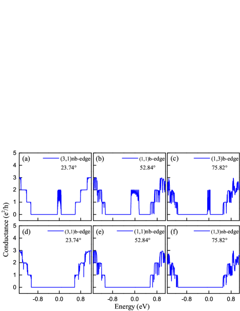
The proposed z-shaped junction in Fig. 4 consists two semi-finite ZPNR electrodes and the central scattering region of a z-shaped PQD. As the degree of torsion of junction is varied, the tilting angle of the center PQD can be altered from 0 to 90∘, hence the whole junction is changed from a standard ZPNR to APNR. However, in this process the two edges of PQD sweep over all possible geometrical morphologies described in Sec. IIB (also see Fig. 1 and Tab. I). As a result the electronic band structure of the PQD varies alternatively between with and without edge states near Fermi energy, and the whole junction is consequently either conducting or semiconducting. In order to explore the variation of the transport for the junction, in Figs. 6(a-f) we first show the calculated conductances (in units of ) for the junction with PQD edges along the three regional boundaries shown in the two sides of Fig. 4, with (3,1)nb-, (1,1)b-, (1,3)b-, (3,1)b-, (1,1)nb- and (1,3)nb-edge, respectively. Apparently, as shown in Figs. 6(a-c), the junction of PQD with (3,1)nb/(1,1)b/(1,3)b-edge exhibits a conductance plateaus of with oscillations within the energy range -0.072/-0.153/-0.095 to 0.072/0.156/0.053 eV due to the edge states Marko . On the contrary, the junction of PQD with (3,1)b-, (1,1)nb- and (1,3)nb-edge, as shown in Figs. 6(d-f), displays almost zero conductance because of the obvious band gap Marko . The result indicates that the edge states of the PQD also play an important role in transport for a z-shaped junction. This interesting transport property has also been reported for a planar homogenous junction formed by graphite ribbons with different edges Katsunori .
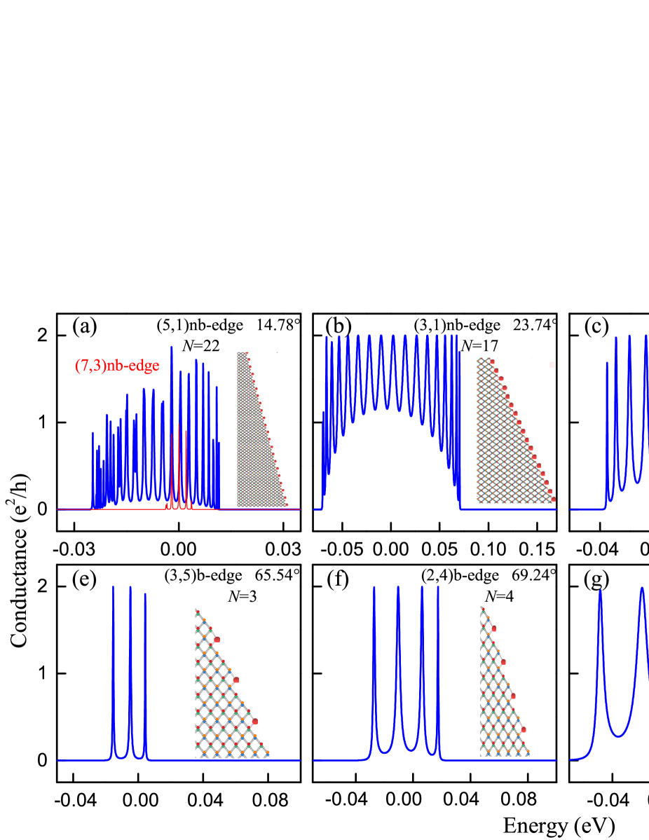
Next, to find the origin of the conductance oscillating peaks, in Fig. 7 we present the low-energy conductance spectra for the junction with in ascending order from 14.78 to 81.38, within which the PQD along directions of (5,1)nb-, (3,1)nb-, (4,2)nb-, (5,3)nb-, (3,5)b-, (2,4)b-, (1,3)b- and (1,5)b-edge are selected, respectively. These eight edges all have an obvious zigzag-like geometry with the enlarged view of edges inserted in each figure. Consistent with the previous the band structure for PNRs with different edges, in Figs. 7(a-d) the conductance spectra for the PQD with four different nonbeard edges all have an oscillating terrace provided by the edge states around the Fermi level. Since the function of the outermost atoms along the zigzag-like configuration are similar to those of actual zigzag-edge, so they are used as a medium atom for electron transport Ezawa . On the other hand, the spectra shown in 7(e-h) respectively for beard (3,5), (2,4), (1,3) and (1,5) edges have a similar feature with an oscillating terrace provided by the edge states. Although these edges with tilting angle close to 90 resulting in the edge atomic configuration similar to armchair type, for the beard SL and its derivative edges still form a periodic zigzag-like configuration due to the outermost dangled phosphorus atoms. This function of the beard edge for PNRs has also been demonstrated previously Ezawa ; Marko .
When the hypotenuse of PQD with edge behind/beyond SZ direction, such as (3,1)nb- and (1,3)b-edge, the junctions exhibit similar transport behavior due to existence of zigzag-like edge geometry. This is because that the outermost phosphorus atom along the zigzag-like edges of PQD form an electronic bound-state Ezawa2 , which is expressed in the energy band as discrete energy levels. These discrete energy levels cause the orphaned electrons at the edge to be hopped to produce an oscillating transport behavior. The function of the outermost atoms along edges can also be well reflected in the conductance spectrum. Interestingly, as clearly shown in Figs. 7(a-h), the number () of the terrace oscillating peaks exactly matches the number of the outermost phosphorus atoms indicated by the (red) dots within an hypotenuse edge of PQD, which is also related to the number of minimum period length along a hypotenuse edge of PQD because that the electrons are localized at each zigzag configuration regardless of which sublayer. Therefore, for a z-shaped junction with certain size, as the edge of the central PQD continuously sweeps over all possible the value of is varied. In addition to the above eight tilting angles, there are many other angles as indicated by the different colored and shaped dots in Fig. 2. The conductance spectrum of the junction with these edge boundaries also exhibits oscillating characteristics in the low energy regime, as shown by the (red) thin lines in Figs. 7(a) and 7(h). For large , the zigzag-like edge may have more inner structures in comparison with those with edges for small . Further, these atomic configurations also produce various scatters that can cause severe interference to the oscillating transport of the electrons, making the discrete levels degenerate and reducing the corresponding conductance. For example, in Fig. 7(a), due to the degeneracy of the energy level and the scattering of the beard edge atomic configurations, the number of conductance peaks is less than that of the outermost phosphorus atoms, and the conductance value is also less than . On the other hand, the value of also limits the conductance. By more calculations, we find that the conductance of the junctions with less than 20 are effective in the low energy regime, otherwise the conductance value is extremely small as is beyond this critical value.
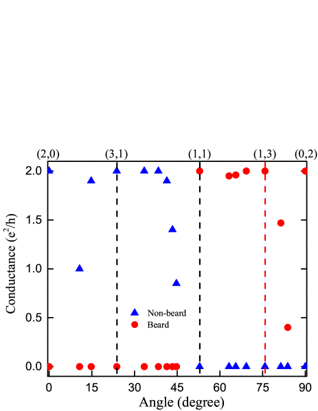
Finally, the data of the calculated conductance vs titling angle for our z-shaped junction whose central PQD with more possible edges with less than critical value 20 are summarized in Fig. 8, where the blue (red) triangles (spheres) for the non-beard (beard) case and the vertical dashed lines indicate the three particular regional boundaries. As the titling (chiral) angle varying from 0 to 90, we can see that the SZ(1,1) at 52.84 is more special, behind/beyond which the conductance is nonzero/zero for the junction with non-beard edges. The situation for the junction with beard edges is just in opposite to the non-beard case, and the two cases are complementary. In addition, more information can be obtained from the phase-like diagram shown in Fig. 8. For instance, the conductance of junction with range from 0 to 90 is between 0 and 2/h sensitively depending on the module length . Since near the three regional boundaries 0 (zigzag), 52.84 (SZ) and 90 (armchair) is more larger, which results in more smaller conductance. This result is in consistence with the distribution of near the bottom of U in Fig. 2. If is beyond this critical value, the conductance tends to zero although there are still edge channels for the junction in the low energy regime.
IV Summary and Conclusion
We have theoretically studied the 2D crystallographic characterization on an anisotropic phosphorene and its applications in nanostructures. A chiral number (vector) or chiral angle is defined to uniformly describe the planar crystallographic directions on a phosphorene. As the chiral angle increasing from 0 to 90, the along boundary edge geometry varies from zigzag to armchair and sweep over all possible edge morphologies during the process. We find a phosphorene can be divided into four fan-shaped regions determined by boundary chiral angles 0, , , and 90, among which the characteristics is different each other. Therefore, by cutting a phosphorene along these five regional boundary directions, one can obtain previously studied ZPNR, SAPNR, SZPNR, and APNR. Importantly, the new type of PNR with SL edge geometry along has been discovered. Essentially, the SL direction is similar to SA one with a periodic zigzag-like edge morphology supporting edge states. Further, we then demonstrate the variation in electronic property for PNRs with different edge atomic geometries by using the Kwant tight-binding (TB) code, in which a particular attention is paid to the new SLPNR intrinsically with twofold-degenerate edge states. In addition, in each regional boundary direction the origin of beard and non-beard edges is discussed and related to the existence of edge states. We find that the (1,1) direction is the dividing line, below/beyand which the ribbon with nonbeard/beard edges.
Second, we propose a two-terminal z-shaped homogenous junction based on PNR and calculate its transport property by using the scattering-matrix for treating large enough systems comparable with experimental samples. The two electrodes of the junction are semi-infinitive ZPNRs with the same width 100 nm, where the central scattering region of a segment of PNR with edge tilting angles from 0 to 90 is sandwiched between them. In consequence the two hypotenuse edges of the central PQD sweep over all possible geometrical morphologies. Interestingly, the conductance spectrum sensitively depends on the tilting angle of z-shaped junction. For the junctions of PQD with edge states the transport exhibit a conductance terrace with resonant oscillation in the low energy regime, otherwise the electron transport is blocked due to the absence of edge states. Remarkably, the number of conductance oscillating peaks is exactly equal to the number of outermost phosphorus atoms in the zigzag-like edges of the center PQD, since the discrete energy levels of the zigzag-like atomic configurations provide the transport channels for electrons. The findings here may be extended to the group-VA 2D materials, such as 2D group-VA arsenene, antimonene and bismuthene, for observing the electronic property of nanostructures in experiments, and provide a reference for the preparation of better nano-devices.
Acknowledgements.
This work was supported by the National Natural Science Foundation of China (Grant Nos. 11774085, 11804092, 11704118), China Postdoctoral Science Foundation funded project (Grant Nos. BX20180097, 2019M652777), and Hunan Provincial Natural Science Foundation of China (Grant No. 2019JJ40187).References
- (1) A. K. Geim and K. S. Novoselov, The rise of graphene, Nat. Mater. 6, 183 (2007).
- (2) Likai Li, Yijun Yu, Guo Jun Ye, Qingqin Ge, Xuedong Ou, Hua Wu, Donglai Feng, Xian Hui Chen and Yuanbo Zhang, Black phosphorus field-effect transistors, Nat. Nanotech. 9, 372 (2014).
- (3) Han Liu, Adam T. Neal, Zhen Zhu, Zhe Luo, Xianfan Xu, David Toma nek, and Peide D. Ye, Phosphorene: an unexplored 2D semiconductor with a high hole mobility, ACS Nano 8, 4033 (2014).
- (4) Fengnian Xia, Han Wang, and Yichen Jia, Rediscovering black phosphorus as an anisotropic layered material for optoelectronics and electronics, Nat. Commun. 5, 4458 (2014).
- (5) Steven P. Koenig, Rostislav A. Doganov, Hennrik Schmidt, A. H. Castro Neto, and Barbaros Özyilmaz, Electric field effect in ultrathin black phosphorus, Appl. Phys. Lett. 104, 103106 (2014).
- (6) Michele Buscema, Dirk J. Groenendijk, Sofya I. Blanter, Gary A. Steele, Herre S. J. van der Zant, and Andres Castellanos-Gomez, Fast and broadband photoresponse of few-layer black phosphorus field-effect transistors, Nano Lett. 14, 3347 (2014).
- (7) Xi Ling, Han Wang, Shengxi Huang, Fengnian Xia, and Mildred S. Dresselhaus, The renaissance of black phosphorus, PNAS 112, 4523 (2015).
- (8) Rishabh Jain, Rekha Narayan, Suchithra Padmajan Sasikala, Kyung Eun Lee, Hong Ju Jung and Sang Ouk Kim, Phosphorene for energy and catalytic application-filling the gap between graphene and 2D metal chalcogenides, 2D Mater. 4, 042006 (2017).
- (9) Pengfei Chen, Neng Li, Xingzhu Chen, Wee-Jun Ong, and Xiujian Zhao, The rising star of 2D black phosphorus beyond graphene: synthesis, properties and electronic applications, 2D Mater. 5, 014002 (2018).
- (10) Chenggang Tao, Liying Jiao, Oleg V. Yazyev, Yen-Chia Chen, Juanjuan Feng, Xiaowei Zhang, Rodrigo B. Capaz, James M. Tour, Alex Zettl, Steven G. Louie, Hongjie Dai, and Michael F. Crommie, Spatially resolving edge states of chiral graphene nanoribbons, Nat. Phys. 7, 610 (2011).
- (11) Y. Li, Z. Zhou, S. Zhang, and Z. Chen, MoS2 nanoribbons: high stability and unusual electronic and magnetic properties, J. Am. Chem. Soc. 130, 16739 (2008).
- (12) Mitchell C. Watts1, Loren Picco, Freddie S. russell-Pavier, Patrick L. Cullen1, thomas S. Miller, Szymon P. Bartuś, Oliver D. Payton, Neal t. Skipper, Vasiliki tileli and Christopher A. Howard, Production of phosphorene nanoribbons, Nature 568, 216 (2019).
- (13) A. Carvalho, A. S. Rodin, and A. H. Castro Neto, Phosphorene nanoribbons, Europhys. Lett. 108, 47005 (2014).
- (14) Marko M. Grujić, Motohiko Ezawa, Milan Ž. Tadić, and Francois M. Peeters, Tunable skewed edges in puckered structures, Phys. Rev. B 93, 245413 (2016)
- (15) Young Woo Son, Marvin L. Cohen and Steven G. Louie, Half-metallic graphene nanoribbons, Nature 444, 16 (2006).
- (16) Vy Tran and Li Yang, Scaling laws for the band gap and optical response of phosphorene nanoribbons, Phys. Rev. B 89, 245407 (2014).
- (17) Ajanta Maity, Akansha Singh, Prasenjit Sen, Aniruddha Kibey, Anjali Kshirsagar, and Dilip G. Kanhere, Structural, electronic, mechanical, and transport properties of phosphorene nanoribbons: negative differential resistance behavior, Phys. Rev. B 94, 075422 (2016).
- (18) Guang Yang, Shenglong Xu, Wei Zhang, Tianxing Ma, and Congjun Wu, Room-temperature magnetism on the zigzag edges of phosphorene nanoribbons, Phys. Rev. B 94, 075106 (2016).
- (19) C. Q. Han, M. Y. Yao, X. X. Bai, Lin Miao, Fengfeng Zhu, D. D. Guan, Shun Wang, C. L. Gao, Canhua Liu, Dong Qian, Y. Liu, and Jin-feng Jia, Electronic structure of black phosphorus studied by angle-resolved photoemission spectroscopy, Phys. Rev. B 90, 085101 (2014).
- (20) Likai Li, Jonghwan Kim, Chenhao Jin, Guojun Ye, Diana Y. Qiu, Felipe H. da Jornada, Zhiwen Shi, Long Chen, Zuocheng Zhang, Fangyuan Yang, Kenji Watanabe, Takashi Taniguchi, Wencai Ren, Steven G. Louie, Xianhui Chen, Yuanbo Zhang, and Feng Wang, Direct observation of the layer-dependent electronic structure in phosphorene, Nat. Nanotech. 12, 21 (2017).
- (21) Sherman Jun Rong Tan, Ibrahim Abdelwahab, Leiqiang Chu, Sock Mui Poh, Yanpeng Liu, Jiong Lu, Wei Chen, and Kian Ping Loh, Quasi-monolayer black phosphorus with high mobility and air stability, Adv. Mater. 30, 1704619 (2018).
- (22) Xianghong Niu, Yunhai Li, Yehui Zhang, Qiang Li, Qionghua Zhou, Jin Zhao, and Jinlan Wang, Photo-oxidative degradation and protection mechanism of black phosphorus: insights from ultrafast dynamics, J. Phys. Chem. Lett. 9, 5034 (2018).
- (23) Xiaoying Zhou, Wen-Kai Lou, Dong Zhang, Fang Cheng, Guanghui Zhou, and Kai Chang, Effective g factor in black phosphorus thin films, Phys. Rev. B 95, 045408 (2017).
- (24) X. Y. Zhou, R. Zhang, J. P. Sun, Y. L. Zou, D. Zhang, W. K. Lou, F. Cheng, G. H. Zhou, F. Zhai, and Kai Chang, Landau levels and magnetotransport property of monolayer phosphorene, Sci. Rep. 5, 12295 (2015).
- (25) Likai Li, Fangyuan Yang, Guo Jun Ye, Zuocheng Zhang, Zengwei Zhu, Wenkai Lou, Xiaoying Zhou, Liang Li, Kenji Watanabe, Takashi Taniguchi, Kai Chang, Yayu Wang, Xian Hui Chen, and Yuanbo Zhang, Quantum Hall effect in black phosphorus two-dimensional electron system, Nat. Nanotech. 11, 592 (2016).
- (26) Ruge Quhe, Qiuhui Li, Qiaoxuan Zhang, Yangyang Wang, Han Zhang, Jingzhen Li, Xiuying Zhang, Dongxue Chen, Kaihui Liu, Yu Ye, Lun Dai, Feng Pan, Ming Lei, and Jing Lu, Simulations of quantum transport in sub-5-nm monolayer phosphorene transistors, Phys. Rev. Appl. 10, 024022 (2018).
- (27) Gautam Gaddemane, William G. Vandenberghe, Maarten L. Van de Put, Shanmeng Chen, Sabyasachi Tiwari, Edward Chen, and Massimo V. Fischetti, Theoretical studies of electronic transport in monolayer and bilayer phosphorene: a critical overview, Phys. Rev. B 98, 115416 (2018).
- (28) Paul Masih Das, Gopinath Danda, Andrew Cupo, William M. Parkin, Liangbo Liang, Neerav Kharche, Xi Ling, Shengxi Huang, Mildred S. Dresselhaus, Vincent Meunier, and Marija Drndic, Controlled sculpture of black phosphorus Nanoribbons, ACS Nano 10, 5687, (2016).
- (29) M. Ezawa, Topological origin of quasi-flat edge band in phosphorene, New J. Phys. 16, 115004 (2014).
- (30) Esmaeil Taghizadeh Sisakht, Mohammad H. Zare, and Farhad Fazileh, Scaling laws of band gaps of phosphorene nanoribbons: A tight-binding calculation, Phys. Rev. B 91, 085409 (2015).
- (31) D. J. P. de Sousa, L. V. de Castro, D. R. da Costa, and J. Milton Pereira, Jr. Boundary conditions for phosphorene nanoribbons in the continuum approach, Phys. Rev. B 94, 235415 (2016).
- (32) SK Firoz Islam, Paramita Dutta, A. M. Jayannavar, and Arijit Saha, Probing decoupled edge states in a zigzag phosphorene nanoribbon via RKKY exchange interaction, Phys. Rev. B 97, 235424 (2018).
- (33) Yi Ren, Fang Cheng, Z. H. Zhang, and Guanghui Zhou, Half metal phase in the zigzag phosphorene nanoribbon, Sci. Rep. 8, 2932 (2018).
- (34) E. Taghizadeh Sisakht, F. Fazileh, M. H. Zare, M. Zarenia, and F. M. Peeters, Strain-induced topological phase transition in phosphorene and in phosphorene nanoribbons, Phys. Rev. B 94, 085417 (2016).
- (35) Benliang Zhou, Benhu Zhou, Xiaoying Zhou and Guanghui Zhou, Even-odd effect on the edge states for zigzag phosphorene nanoribbons under a perpendicular electric field, J. Phys. D: Appl. Phys. 50, 045106 (2017).
- (36) Xiaoyu Han, Henry Morgan Stewart, Stephen A. Shevlin, C. Richard A. Catlow, and Zheng Xiao Guo, Strain and orientation modulated bandgaps and effective masses of phosphorene nanoribbons, Nano Lett. 14, 4607 (2014).
- (37) R. Ma, H. Geng, W. Y. Deng, M. N. Chen, L. Sheng, and D. Y. Xing, Effect of the edge states on the conductance and thermopower in zigzag phosphorene nanoribbons, Phys. Rev. B 94, 125410 (2016).
- (38) Zahra Nourbakhsh1 and Reza Asgari, Charge transport in doped zigzag phosphorene nanoribbons, Phys. Rev. B 97, 235406 (2018).
- (39) L. L. Li, and F. M. Peeters, Quantum transport in defective phosphorene nanoribbons: effects of atomic vacancies, Phys. Rev. B 97, 075414 (2018).
- (40) S. Soleimanikahnoj and I. Knezevic, Pseudospin electronics in phosphorene nanoribbons, Phys. Rev. Appl. 8, 064021 (2017).
- (41) A. R. Akhmerov and C. W. J. Beenakker, Boundary conditions for Dirac fermions on a terminated honeycomb lattice, Phys. Rev. B 77, 085423 (2008).
- (42) Te-Huan Liu, Yin-Chung Chen, Chun-Wei Pao, and Chien-Cheng Chang, Anisotropic thermal conductivity of MoS2 nanoribbons: Chirality and edge effects, Appl. Phys. Lett. 104, 201909 (2014).
- (43) Ashwin Ramasubramaniam, Andre R. Muniz, Ab initio studies of thermodynamic and electronic properties of phosphorene nanoribbons, Phys. Rev. B 90, 085424 (2014).
- (44) Yuanyue Liu, Fangbo Xu, Ziang Zhang, Evgeni S. Penev, and Boris I. Yakobson, Two-dimensional mono-elemental semiconductor with electronically inactive defects: the case of phosphorus, Nano Lett. 14, 6782 (2014).
- (45) Liangbo Liang, Jun Wang, Wenzhi Lin, Bobby G. Sumpter, Vincent Meunier, and Minghu Pan, Electronic bandgap and edge reconstruction in phosphorene materials, Nano Lett. 14, 6400 (2014).
- (46) See Supplemental Material at [ ] for detailed discussion on the classification of crystal directions.
- (47) Vladimir V. Arsoski, Marko M. Grujić, Nemanja A. Čukarić, Milanž. Tadić, and Francois M. Peeters, Normal and skewed phosphorene nanoribbons in combined magnetic and electric fields, Phys. Rev. B 96, 125434 (2017).
- (48) Z. T. Lv, J. H. Gao, X. D. Zhang and Z. T. Jiang, Coupling and manipulation of edge states in multilayer phosphorene nanoribbons, Physica E, 94, 59 (2017).
- (49) C. W. Groth, M. Wimmer, A. R. Akhmerov, and X. Waintal, Kwant: a software package for quantum transport, New J. Phys. 16, 063065 (2014).
- (50) Shengli Zhang, Shiying Guo, Zhongfang Chen, YeliangWang, Hongjun Gao, Julio Gómez-Herrero, Pablo Ares, Fe lix Zamora, Zhen Zhu and Haibo Zeng, Recent progress in 2D group-VA semiconductors: from theory to experiment, Chem. Soc. Rev. 47, 982 (2018).
- (51) Yongjin Jiang and Liangbin Hu, Symmetry properties of spin currents and spin polarizations in multiterminal mesoscopic spin-orbit-coupled systems, Phys. Rev. B 75, 195343 (2007).
- (52) M. Zwierzycki, P. A. Khomyakov, A. A. Starikov, K. Xia, M. Talanana, P. X. Xu, V. M. Karpan, I. Marushchenko, I. Turek, G. E. W. Bauer, G. Brocks, and P. J. Kelly, Calculating scattering matrices by wave function matching, Phys. Stat. Sol. B 245, 623 (2008).
- (53) Tatiane P. Santos, Leandro R. F. Lima, Caio H. Lewenkopf, An order N numerical method to efficiently calculate the transport properties of large systems: An algorithm optimized for sparse linear solvers, J. Comput. Phys. 394, 440 (2019).
- (54) Pengke Li and Ian Appelbaum, Electrons and holes in phosphorene, Phys. Rev. B 90, 115439 (2014).
- (55) A. N. Rudenko and M. I. Katsnelson, Quasiparticle band structure and tight-binding model for single- and bilayer black phosphorus, Phys. Rev. B 89, 201408(R) (2014).
- (56) Yea-Lee Lee, Fangzhou Zhao, Ting Cao, Jisoon Ihm, and Steven G. Louie, Topological Phases in Cove-Edged and Chevron Graphene Nanoribbons: Geometric Structures, Z2 Invariants, and Junction States, Nano Lett. 18, 7247 (2018).
- (57) Z. F. Wang, Qunxiang Li, Q. W. Shi, Xiaoping Wang, J. G. Hou, Huaixiu Zheng and Jie Chen, Ballistic rectification in a Z-shaped graphene nanoribbon junction, Appl. Phys. Lett. 92, 133119 (2008).
- (58) Rui Zhang, X. Y. Zhou, D. Zhang, W. K. Lou, F. Zhai and Kai Chang, Electronic and magneto-optical properties of monolayer phosphorene quantum dots, 2D Mater. 2, 045012 (2015).
- (59) Rui Zhang, Zhenhua Wu, X. J. Li, and Kai Chang, Aharonov-Bohm effect in monolayer phosphorene nanorings, Phys. Rev. B 95, 125418 (2017).
- (60) Enrique Montes and Udo Schwingenschlögl, High-performance field-effect transistors based on P and P, Adv. Mater. 31, 1807810 (2019).
- (61) Katsunori Wakabayashi and Manfred Sigrist, Zero-Conductance resonances due to flux states in nanographite ribbon junctions, Phys. Rev. Lett. 84, 3390 (2000).
- (62) Anffany Chen, R. Ilan, F. de Juan, D. I. Pikulin, and M. Franz, Quantum holography in a graphene flake with an irregular boundary, Phys. Rev. lett. 121, 036403 (2018).
- (63) S. Datta, Electronic transport in mesoscopic systems (Cambridge University Press, Cambridge, 1995).
- (64) Motohiko Ezawa, Minimal models for Wannier-type higher-order topological insulators and phosphorene, Phys. Rev. B 98, 045125 (2018).