Aharonov-Bohm oscillations of four-probe resistance in topological quantum rings in silicene and bilayer graphene
Abstract
We consider observation of Aharonov-Bohm oscillations in clean systems based on the flow of topologically protected currents in silicene and bilayer graphene. The chiral channels in these materials are defined by the flips of the vertical electric field. The line of the flip confines chiral currents flowing along it in the direction determined by the valley. We present an electric field profile that forms a crossed ring to which four terminals can be attached, and find that the conductance matrix elements oscillate in the perpendicular magnetic field in spite of the absence of backscattering. We propose a four-probe resistance measurement setup, and demonstrate that the resistance oscillations have large visibility provided that the system is prepared in such a way that a direct transfer of the chiral carriers between the current probes is forbidden.
I Introduction
In III-V systems with the two-dimensional electron gas the Aharonov-Bohm interferometers are formed by definition of gated channels forming ring-like structures by etching Strambini et al. (2009) or surface oxidation Fuhrer et al. (2001). Quantum rings are also defined in graphene by etching Cabosart et al. (2014). In the etched systems disorder and resulting electron backscattering within the arms of the ring are usually present which lowers the visibility of the Aharonov-Bohm conductance oscillations Szafran and Poniedziałek (2009). In the present work we consider Aharonov-Bohm interferometers with arms formed by chiral Katsnelson et al. (2006) channels that are protected against backscattering by symmetry constraints.
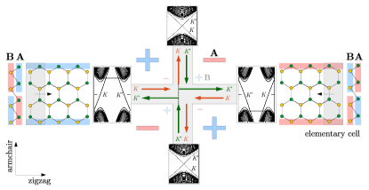
Graphene A.H. Castro Neto et al. (2009) nanoribbon K. Wakabayashi et al. (2009) with zigzag edges forms a perfect chiral channel for low Fermi energy. The Fermi wave vectors corresponding to the current flow in one direction or the other appear in opposite valley states Nakada et al. (1996); Wakabayashi (2001); Peres et al. (2006). The chiral Katsnelson et al. (2006) valley current within a quasi one-dimensional channel is protected against backscattering by a smooth potential variation. Only potential defects that are short range on the scale of the lattice constant can induce intervalley transition that implies backscattering Nakada et al. (1996); Wakabayashi (2001); Peres et al. (2006). However, formation of a quantum ring of purely zigzag edges is unlikely. For that reason we consider chiral channels defined within the bulk of the sample by gating. In staggered monolayer graphene Yao et al. (2009); Cheng et al. (2018), in buckled silicene lattice Aufray et al. (2010); Liu et al. (2011a, b); Chowdhury and Jana (2016), or other 2D Xene materials Molle et al. (2017); Cahangirov et al. (2009); Xu et al. (2013), the chiral channels for the electron flow can be tailored by a symmetry breaking potential along its zero lines Yao et al. (2009); Ezawa (2012a); Szafran et al. (2019). For buckled silicene Aufray et al. (2010); Liu et al. (2011a, b); Chowdhury and Jana (2016) – a hexagonal crystal with the two sublattices placed on two parallel planes – the symmetry breaking potential is introduced by perpendicular electric field Ezawa (2012a); Szafran et al. (2019). Similar chiral channels appear in bilayer graphene Martin et al. (2008); Qiao et al. (2011); Zarenia et al. (2011); Ju et al. (2015); Li et al. (2016); Cheng et al. (2018) along the flip of the vertical electric field or in bilayer graphene at the / stacking interface induced by a dislocation Ju et al. (2015); Vaezi et al. (2013) or twist of the layers Bistritzer and MacDonald (2011); Xu et al. (2019). The / interfaces in twisted bilayer graphene form a triangular lattice with the direction of the current flow opposite for both valleys Xu et al. (2019); Efimkin and MacDonald (2018); Rickhaus et al. (2018).
Recently, a ring-like system with splittings of the chiral zero-line channels was proposed for both silicene and bilayer graphene Szafran et al. (2019). The electron passage time across this system is a periodic function of the external magnetic field due to the Aharonov-Bohm phase difference accumulated from the vector potential Szafran et al. (2019). However, the two-terminal Landauer conductance of these systems is independent of the external magnetic field, since the backscattering is absent due to the valley protection. In order to observe the Aharonov-Bohm oscillations in two-terminal conductance one should rely on atomic-scale disorder. The atomic disorder is hard to control and electron interferometers should be difficult to construct in this way.
The message of this paper is that one can design a four-terminal interferometer device for the observation of the Aharonov-Bohm oscillations of conductance for clean chiral channels defined in both silicene and bilayer graphene that works in absence of the electron backscattering. We study the chiral current flow in the channels formed by the electric potential flips that define the four-terminal crossed-quantum ring in silicene and bilayer graphene. A simulation of two nonequivalent four-point resistance measurement setups is perfomed. We find a distinct Aharonov-Bohm periodicity in the resistance amplitude that is associated with the interference on 1/4 of the ring area. We discuss the interference paths that are behind this periodicity.
II Theory
II.1 Silicene
In this work we use the atomistic tight-binding Hamiltionian spanned by orbitals Liu et al. (2011b); Ezawa (2012b); Chowdhury and Jana (2016)
| (1) |
where stands for the nearest neighbor ions. The () is the creation (annihilation) operator for an electron on site , and eV is the hopping parameter Liu et al. (2011b); Ezawa (2012b). We introduce the magnetic field via the Peierls phase in the term, where with the vector potential . The crystal lattice vectors and define the positions of the ions of the subblatice, where the silicene lattice constant Å, and , are integers, and the ions of the sublattice are shifted by the basis vector , where Å is the nearest neighbor in-plane distance and Å is the vertical shift between the sublattice planes.
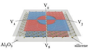
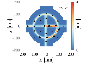
The quantum ring with the chiral channels is formed by the electric field induced by the split top and bottom gates [Fig. 1(a)]. The systems of multiple dual gates below and above the two dimensional crystals are used to modify the local electron structure Soleimanikahnoj and Knezevic (2017); Tayari et al. (2016); Banerjee et al. (2009); Rickhaus et al. (2018). The inversion of the field creates a topologically protected conducting channel. We consider a ring of radius with the center at the origin formed by the model potential
| (2) |
where is the distance from the origin, is the gate potential and is the parameter responsible for the inversion length. For symmetric gating the potential on the sublattice is opposite .
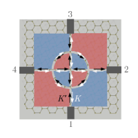
In Fig. 1(b) we plot the direction of the current channels that are open for the and valley electron flow. The valley electrons move along the zero line of the potential given by Eq. (2) leaving the region of negative potential on the sublattice on the left hand-side. Note that the current injected from terminal zero-line 1 can be directed to either terminal 2 or terminal 4. In terminal 3 there is no valley state that carries the electron flow up, away from the ring (Fig. 2). In every channel the direction of the current flow for the valley (with respect to the ) is opposite.
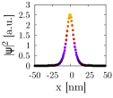
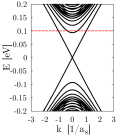
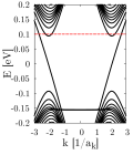
The wave function of the states confined laterally at the zero line near is plotted in Fig. 3(a). The confined states correspond to linear bands that appear within the energy gap [Fig. 3(b)].

II.2 Bilayer graphene
For bilayer graphene the inversion-symmetry-breaking potential can be introduced by an electric field perpendicular to the sheet. We consider a bilayer-graphene-based system analogous to the one described in Sec. II.1, with the difference that due to the presence of two layers, two topological states occur instead of one as in silicene. We consider the tight-binding Hamiltonian similar as in Eq. (1)
| (3) |
with graphene lattice constant Å, the interlayer distance of Å and the tight-binding parameters of bilayer graphene with Bernal stacking Partoens and Peeters (2006), where eV for the nearest neighbors within the same layer, and for the interlayer coupling, eV for the dimers, eV for the skew hoppings between atoms of the same sublattice, and eV – between the atoms of different sublattices.
The model potential in the lower layer is described by a formula analogous as in Eq. (2), and in the upper layer it has the opposite polarization, but the sign is the same in both sublattices within the same layer. We use nm, nm, and meV.
II.3 Landauer approach
We solve the electron scattering problem formed in the tight binding model with the wave-function matching (WFM) technique. The details of the method were described in Refs. Kolasiński et al. (2016); Rzeszotarski and Szafran (2018). The electron transfer probability is calculated as
| (4) |
where denote the probability amplitude for the transfer from incoming mode in the input lead to outgoing mode in the output lead . Thus, the Landauer conductance formula for the transfer from lead to can be written as
| (5) |
where is the flux quantum.
We focus our attention on the Fermi level eV and take into account the spin degree of freedom so that all the assumptions provide for silicene, and for bilayer graphene.
II.4 Conductance matrix
The scattering problem for the four-terminal system was solved for each lead as an input channel and the results were collected in the conductance matrix with the general form
| (6) |
with . Due to the rotational symmetry ( in terms of channel shape) the conductance matrix can be put in the form
| (7) |
where the coefficients
| (8) | |||
| (9) | |||
| (10) |
and .
Assuming that we can truncate the 3rd column Datta (1995) and calculate the resistance matrix that can be written as follows
| (11) |
with matrix determinant that is always positive.
II.5 4-point resistance measurement
We consider two configurations of resistance measurement (Fig. 4) in the system with varied voltage and current terminals.
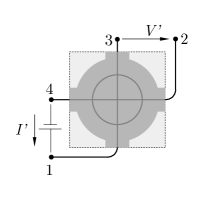
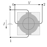
For the first configuration from Fig. 4(a) the resistance is calculated as
| (12) |
and for the other [Fig. 4(b)],
| (13) |
III Results and Discussion
III.1 Small ring
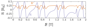
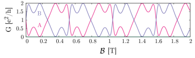
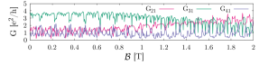
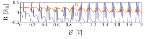
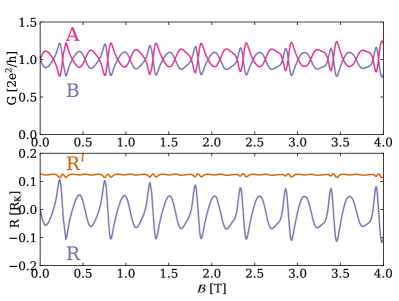
In this subsection for the silicene system we use meV and nm. In Fig. 5 and 6 we plotted the results for the conductance matrix elements (upper plots) and the resistances and (lower plots) for meV and meV, respectively. The oscillations of the matrix elements that have nearly maximal amplitude are translated to oscillations of resistance that have high () or low () visibility.
The current probe terminals for configuration correspond to an open direct current path. The resistance has a constant sign since the numerator in Eq. (12) is always nonnegative .
For configuration the current from terminal 1 can reach the terminal 3 only via the voltage terminals 2 and 4 which absorb the current and send an equal current back in the opposite valley, which is necessary to keep the net current at the voltage probes equal to zero. The resistance changes sign [Fig. 5(b) and Fig. 6(b)] as the magnetic field is varied. From Eq. (13), since the determinant is positive, the sign change needs to be accompanied by the sign change of the difference (or the matrix elements ). Hence, the changes of sign of appear when the electron transfer probability from terminal 1 to 4 crosses the electron transfer probability in the opposite direction. The directions become non-equivalent from the point of view of the electron transfer when the external magnetic field is introduced.
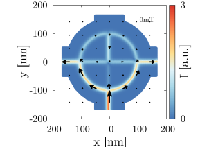
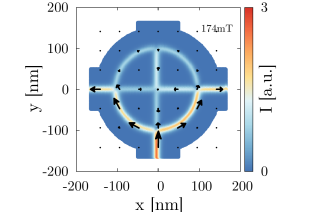
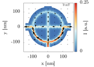
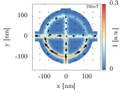
The current circulation paths for meV are presented in Fig. 7. For magnetic fields such that Fig. 5(a), the current is evenly distributed from terminal 1 to the left and the right leads (Fig. 7(a,c)), while for stationary points (Fig. 7(b,d,e,f)) one can distinguish current loops around quarters of the ring.
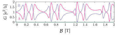
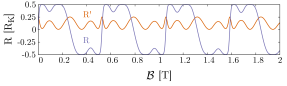
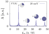
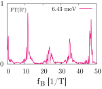
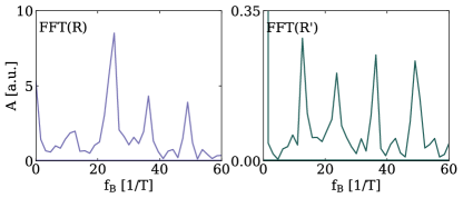
By taking the Fourier transform of the resistance and (from Fig. 5(b) and 6(b), respectively) for magnetic field range from 0 to 40 T we can distinguish 4 characteristic peaks (Fig. 8) associated to periods () respectively. For each period the area can be calculated as , and using the Aharonov-Bohm formula for period we obtain
| (14) |
In our calculations the channel ring has radius nm and area , hence
| (15) |
is the fraction of the ring area responsible for the Aharonov-Bohm interference. Thus, taking the list from the Fourier transform we obtain
for peaks 1 – 4 from left to right in Fig. 8, respectively. The leftmost peak that corresponds to the interference paths that encircle a quarter of the ring is the most pronounced. In the current distribution in Fig. 7 one can indicate the paths that encircle a few quarters of the ring, but the fundamental period corresponds to 1/4 of the ring.
III.2 Larger ring, nonchiral bands, weaker vertical field
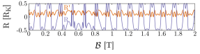
The clear Aharonov-Bohm oscillations of the resistance presented above were obtained for a system with a relatively small radius, narrow flip length and a very strong vertical electric field with only chiral bands at the Fermi level.
Let us consider a system with larger field inversion length increased from nm to nm and meV, for which nonchiral modes appear at the Fermi level (Fig. 9). The results for the conductance matrix elements and the resistance are plotted in Fig. 10(a). The non-chiral currents transfer across the ring from lead 1 to 3, see (Fig. 10(a)), which is forbidden for the chiral bands. In presence of the nonchiral bands the conductance matrix has no longer the form given by Eq. (7) and a general formula needs to be applied to calculate the resistances and by inverting the conductance matrix. The results of and calculations are presented in Fig. 10(b). Matching peaks (dips) to a periodic pattern we observe periodicity of the plot with mean spacing of 66 mT and 131 mT, which for nm correspond to flux quantum threading 1/2 and 1/4 of the ring area, respectively. In the presence of the nonchiral bands, the amplitude of the oscillations becomes comparable to the ones of .
For the same parameters nm and nm but a lower Fermi level meV (see Fig. 9) we reproduce the regular oscillations (Fig. 11) of the purely chiral case presented above for nm and nm.
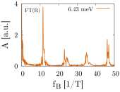
The assumed potential of eV at each sublattice of the buckled silicene requires a giant vertical field of the order of 10 V/nm. The vertical field applied for two-dimensional crystals can be very large without inducing the breakdown due to atomic width of the system. However, the fields considered for the silicene Ni et al. (2011) and the ones applied to bilayer-graphene Rickhaus et al. (2018); Zhang et al. (2009) are of the order of 1 V/nm only. In order to verify that the effects described above can be observed for similar electric fields we performed calculations for 10 times weaker gate potential meV at meV for nm and nm with only the single linear chiral mode at the Fermi level. The Aharonov-Bohm oscillations can be resolved in and dependence on the magnetic field (Fig. 12), with the larger visibility of the oscillations as above.

IV Bilayer-graphene-based system
For bilayer graphene system the results are qualitatively similar as for silicene, with the difference that for the Fermi energy within the energy gap we have max, as the number of topological states is doubled due to the presence of two layers. This can be seen in the band structure of the armchair input leads in Fig. 13(d). For the zigzag leads, Fig. 13(a, b, c), within the energy gap the edge states occur that, however, do not contribute to the inter-lead conductance. and is always equal to 2, with the edge modes being completely backscattered, and only the flip-modes leaving the zigzag leads.
Fig. 14 shows the current distribution in the bilayer graphene system for meV for the electron incident from the lower lead. As in silicene, the current cannot pass to the upper lead. Instead, we observe only the transfer to one of the two nearest leads. For [Fig. 14(a) and (b)] the current is evenly distributed within the system, while at the extrema of and [Fig. 14(c) and (d)] the current distribution is asymmetric, and loops around quarters of the ring are more pronounced.
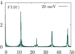
The conductance matrix elements in Fig. 15(a), and the resistance in Fig. 15(b) manifest oscillations of the periodicity corresponding to a single or several quarters of the ring as for silicene. In the Fourier transform of the resistance in Fig. 16(a) and (b) we find peaks at the frequencies associated with the periods () respectively. These correspond roughly to the area of one, two, three, or four quarters of the ring, respectively.
V Summary and conclusions
We have studied Aharonov-Bohm interferometers with chiral channels defined by inversion of the vertical electric field in silicene and bilayer graphene. The valley protected channels induced by inhomogeneous electric field in silicene and bilayer graphene in clean conditions i.e. without the backscattering (due to the intervalley transitions) can serve for the observation of the Aharonov-Bohm oscillations provided that four (instead of two) terminals are attached to the system. The Aharonov-Bohm oscillations of four-probe resistance with large visibility are observed when a direct electron transfer between terminals (chosen as the current probes) is forbidden. The fundamental period of the resistance oscillations corresponds to a quarter of the ring, or to the smallest loop that a chiral current encircles within the structure.
Acknowledgments
B.R. is supported by Polish government budget for science in 2017-2021 as a research project under the program "Diamentowy Grant" (Grant No. 0045/DIA/2017/46), by the EU Project POWR.03.02.00-00-I004/16 and NCN grant UMO-2019/32T/ST3/00044. A.M-K. is supported with "Diamentowy Grant" (Grant No. 0045/DIA/2017/46). The calculations were performed on PL-Grid Infrastructure on Rackserver Zeus at ACK-AGH Cyfronet.
References
- Strambini et al. (2009) E. Strambini, V. Piazza, G. Biasiol, L. Sorba, and F. Beltram, Phys. Rev. B , 195443 (2009).
- Fuhrer et al. (2001) A. Fuhrer, S. Lüscher, T. Ihn, T. Heinzel, K. Ensslin, W. Wegscheider, and M. Bichler, Nature 413, 822 (2001).
- Cabosart et al. (2014) D. Cabosart, S. Faniel, F. Martins, B. Brun, A. Felten, V. Bayot, and B. Hackens, Phys. Rev. B 90, 205433 (2014).
- Szafran and Poniedziałek (2009) B. Szafran and M. R. Poniedziałek, Phys. Rev. B 80, 155334 (2009).
- Katsnelson et al. (2006) M. Katsnelson, K. Novoselov, and A. K. Geim, Nature Phys. 2, 620 (2006).
- A.H. Castro Neto et al. (2009) F. A.H. Castro Neto, Guinea, N. M. R. Peres, K. Novoselov, and A. K. Geim, Rev. Mod. Phys. 81, 109 (2009).
- K. Wakabayashi et al. (2009) Y. K. Wakabayashi, Takane, M. Yamamoto, , and M. Sigrist, New. J. Phys 11, 095016 (2009).
- Nakada et al. (1996) K. Nakada, M. Fujita, G. Dresselhaus, , and M. S. Dresselhaus, Phys. Rev. B 54, 17954 (1996).
- Wakabayashi (2001) K. Wakabayashi, Phys. Rev. B 64, 125428 (2001).
- Peres et al. (2006) N. M. R. Peres, A. H. Castro Neto, and F. Guinea, Phys. Rev. B 73, 195411 (2006).
- Yao et al. (2009) W. Yao, S. Yang, , and Q. Niu, Phys. Rev. Lett. 102, 096801 (2009).
- Cheng et al. (2018) S.-g. Cheng, H. Liu, H. Jiang, Q.-F. Sun, and X. C. Xie, Phys. Rev. Lett. 121, 156801 (2018).
- Aufray et al. (2010) B. Aufray, A. Kara, S. Vizzini, H. Oughaddou, C. Léandri, B. Ealet, and G. L. Lay, Applied Physics Letters 96, 183102 (2010).
- Liu et al. (2011a) C.-C. Liu, W. Feng, and Y. Yao, Phys. Rev. Lett. 107, 076802 (2011a).
- Liu et al. (2011b) C.-C. Liu, H. Jiang, and Y. Yao, Phys. Rev. B 84, 195430 (2011b).
- Chowdhury and Jana (2016) S. Chowdhury and D. Jana, Reports on Progress in Physics 79, 126501 (2016).
- Molle et al. (2017) A. Molle, J. Goldberger, M. Houssa, Y. Xu, S.-C. Zhang, and D. Akinwande, Nature Materials 16, 163 (2017).
- Cahangirov et al. (2009) S. Cahangirov, M. Topsakal, E. Aktürk, H. Şahin, and S. Ciraci, Phys. Rev. Lett. 102, 236804 (2009).
- Xu et al. (2013) Y. Xu, B. Yan, H.-J. Zhang, J. Wang, G. Xu, P. Tang, W. Duan, and S.-C. Zhang, Phys. Rev. Lett. 111, 136804 (2013).
- Ezawa (2012a) M. Ezawa, New Journal of Physics 14, 033003 (2012a).
- Szafran et al. (2019) B. Szafran, B. Rzeszotarski, and A. Mreńca-Kolasińska, Phys. Rev. B 100, 085306 (2019).
- Martin et al. (2008) I. Martin, Y. M. Blanter, and A. F. Morpurgo, Phys. Rev. Lett. 100, 036804 (2008).
- Qiao et al. (2011) Z. Qiao, J. Jung, Q. Niu, , and A. MacDonald, Nano Lett. 11, 3453 (2011).
- Zarenia et al. (2011) M. Zarenia, J. M. Pereira Jr., G. Farias, , and F. M. Peeters, Phys. Rev. B 84, 125451 (2011).
- Ju et al. (2015) L. Ju, Z. Shi, N. Nair, Y. Lv, C. Jin, J. Velasco Jr, C. Ojeda-Aristizabal, H. Bechtel, M. Martin, A. Zettl, J. Analytis, and F. Wang, Nature 520, 650 (2015).
- Li et al. (2016) J. Li, K. Wang, K. McFaul, Z. Zern, Y. Ren, K. Watanabe, T. Taniguchi, Z. Qiao, , and J. Zhu, Nature Nano. 11, 1060 (2016).
- Vaezi et al. (2013) A. Vaezi, Y. Liang, D. Ngai, L. Yang, and E.-A. Kim, Phys. Rev. X 3, 021018 (2013).
- Bistritzer and MacDonald (2011) R. Bistritzer and A. H. MacDonald, Proc. Natl. Acad. Sci. 108, 12233 (2011).
- Xu et al. (2019) S. G. Xu, A. I. Berdyugin, P. Kumaravadivel, F. Guinea, R. Krishna Kumar, D. A. Bandurin, S. Morozov, W. Kuang, B. Tsim, S. Liu, J. Edgar, I. Grigorieva, V. I. Fal’ko, M. Kim, and A. K. Geim, Nature Comm. 10, 4008 (2019).
- Efimkin and MacDonald (2018) D. K. Efimkin and A. H. MacDonald, Phys. Rev. B 98, 035404 (2018).
- Rickhaus et al. (2018) P. Rickhaus, J. Wallbank, S. Slizovskiy, R. Pisoni, H. Overweg, Y. Lee, M. Eich, M.-H. Liu, K. Watanabe, T. Taniguchi, T. Ihn, and K. Ensslin, Nano Letters 18, 6725 (2018).
- Ezawa (2012b) M. Ezawa, Phys. Rev. Lett. 109, 055502 (2012b).
- Soleimanikahnoj and Knezevic (2017) S. Soleimanikahnoj and I. Knezevic, Phys. Rev. Applied 8, 064021 (2017).
- Tayari et al. (2016) V. Tayari, N. Hemsworth, O. Cyr-Choinière, W. Dickerson, G. Gervais, and T. Szkopek, Phys. Rev. Applied 5, 064004 (2016).
- Banerjee et al. (2009) S. K. Banerjee, L. F. Register, E. Tutuc, and A. H. Macdonald, IEEE Electron Device Letters 30, 158 (2009).
- Partoens and Peeters (2006) B. Partoens and F. M. Peeters, Phys. Rev. B 74, 075404 (2006).
- Kolasiński et al. (2016) K. Kolasiński, B. Szafran, B. Brun, and H. Sellier, Phys. Rev. B 94, 075301 (2016).
- Rzeszotarski and Szafran (2018) B. Rzeszotarski and B. Szafran, Phys. Rev. B 98, 075417 (2018).
- Datta (1995) S. Datta, Electronic Transport in Mesoscopic Systems (Cambridge University Press, 1995).
- Ni et al. (2011) Z. Ni, Q. Liu, K. Tang, J. Zheng, J. Zhou, R. Qin, Z. Gao, D. Yu, and J. Lu, Nano Letters 12, 113 (2011).
- Zhang et al. (2009) Y. Zhang, T. Tang, G. C, Z. Hao, M. C. Martin, Z. A., M. Crommie, Y. Shen, and F. Wang, Nature 459, 820 (2009).