Observation of excess resistance anomaly at resistive transitions in Ag/Au nanostructures
Abstract
The resistive transition in nanocomposite films of silver (Ag) nanoclusters of nm diameter embedded in gold (Au) matrix exhibits an anomalous resistance peak at the onset of the transition, even for transition temperatures as high as 260 K. The maximum value of the resistance ranges between above that of the normal state depending on devices as well as lead configuration within a single device. The excess resistance regime was observed in about % of the devices, and extends from K. Application of magnetic field of 9 T was found to partially suppress the excess resistance. From the critical current behavior, as well as negative differential resistance in the current-voltage characteristics, we discuss the possibility of interacting phase slip centers and alternate physical scenarios that may cause the excess resistance in our system.
# These authors contributed equally.
Occurrence of anomalous resistance peak at the onset of superconducting transition is one of the most ubiquitous phenomenon observed in many disordered superconductors ranging from metals, high ceramics to granular superconductors realized with bottom-up synthesis approach berlincourt1959hall ; grassie1970transition ; ems1971resistance ; tajima1984magnetic ; tajima1984giant ; yamamoto1985giant ; lindqvist1990new ; crusellas1992giant ; santhanam1991resistance ; wan1993interlayer ; vaglio1993explanation ; suzuki1994resistance ; moshchalkov1994intrinsic ; mosqueira1994resistivity ; park1995resistance ; silva1997microwave ; park1997resistance ; strunk1998resistance ; arutyunov1999resistive ; buzea2001origin ; wang2007observation ; harada2010large ; zhang2013metal . Although a generic explanation remains elusive, appearance of such anomalies is attributed to geometric and/or non-equilibrium effects at the normal-superconductor interfaces in the presence of structural and compositional inhomogeneities (arutyunov1999resistive, ; park1997resistance, ; crusellas1992giant, ; lindqvist1990new, ). A transition to vanishingly small electrical resistance state and the concurrent emergence of diamagnetic susceptibility have recently been observed in nanocomposite films of Ag nanoclusters ( nm diameter) dispersed on Au matrix close to room temperature, suggesting possible emergence of superconductor-like macroscopic coherence at elevated temperatures thapa2018coexistence . The current ()-voltage () characteristics in these films near the resistive transition was also reported to exhibit critical current behavior with strong hysteresis and discrete resistance steps islam2019current . This was attributed to a highly non-equilibrium nature of the quasi-particle transport and filamentary flow of supercurrent through dissipative phase slip centres (PSC) close to the transition. Counterarguments based on weak-links urazhdin2019comment and percolative decoupling of current and voltage leads pekker2018comment have also been proposed, prompting further experimentation on the nature of current flow in this unique system. In this paper, we report the observation of excess resistance anomaly in Ag/Au nanostructure film in a multi-terminal geometry at the onset of the resistive transition. We also find that below the transition temperature, the characteristics exhibit current-driven sequential voltage-peaks and negative differential resistances (NDR). The anomaly is partially suppressed at high magnetic field, and bears close resemblance to its key characteristics at the conventional normal-superconductor transitions arutyunov1999resistive ; lindqvist1990new ; kwong1991interfacial ; crusellas1992giant ; zhang2013metal .
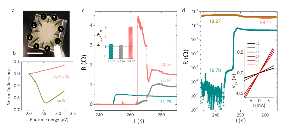
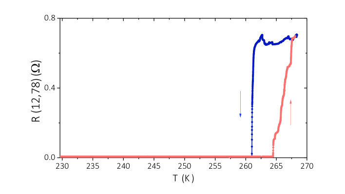
The Ag/Au nano-structure films were made by planting Ag nano-particles ( nm) into a gold matrix using colloidal technique thapa2018coexistence ; islam2019current ; thapa2019unconventional . Briefly, silver clusters were prepared by the reduction of silver nitrate in cetyltrimethylammonium bromide with sodium borohydride. Gold was then introduced in the form of tetrachloroauric acid. Multiple layers of the film ( nm) were dropcast on pre-patterned nm Cr/Au-electrical contacts on glass substrate arranged in van der Pauw geometry as shown in Fig. 1a. Fig. 1b shows the normalized optical reflectance from a typical flim over the energy range of eV, and compared with that from a reference Au-nanoparticle film. The absence of plasmonic absorption at eV is one of the key features of the Ag/Au nanostructures. A detailed discussion of this process as well as its optical properties have been reported elsewhere thapa2018coexistence ; thapa2019unconventional . Fig. 1c shows the temperature dependence of four-probe resistance () measured with a constant bias current of mA in different current-voltage contact configurations across the sample. The four-probe for ( and ) and channels were recorded simultaneously in the same thermal cycle, while that for with rotated lead configuration was measured in a separate cool down. The resistance of the as-prepared films varies from across the different regions of the film with corresponding resistivity -m islam2019current . As evident from Fig. 1c, the resistive transition occurs between K, although both transition temperature () and its nature (e.g. width) depend strongly on the lead configuration. In some transitions, a residual resistance of m at was observed, possibly due to the granular nature of the film or weak coupling to the leads, and subtracted manually. We also observed a strong hysteresis between the cooling and the heating cycles (supplementary information), and unless specified otherwise , the data presented here are from the heating cycles.
In order to verify inter-connectivity between all the leads across the transition, and absence of any unintended constriction due to -dependent structural changes, we have measured () for various current-voltage lead configurations between and , and () two-probe current-voltage characteristics between all pairwise lead combinations. As shown in Fig. 1d, in spite of nearly four decades of change in resistance in the channel at K, the and channels remain essentially unaffected, suggesting (1) absence of any major structural modification in the region between the lead pairs (,) and (,) as a function of , and (2) the physical location of the low resistance/superconducting filament across leads ( and ) and/or ( and ). The metallic inter-connectivity between the leads is further ensured from linear two-probe characteristics between all lead pairs (inset of Fig. 1d).
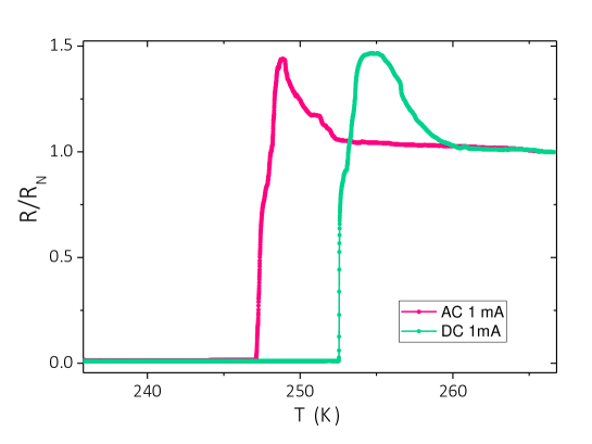
In Fig. 1c, in all three lead configurations exhibits an increase in magnitude K before transition to the low resistance state. Such an increase was observed in % of the devices that showed the resistive transition. This anomalous increase in , characterized by the ratio of maximum in resistance close to and that () at varies between for different regions of the sample (Fig. 1c inset). The increase was observed irrespective of the AC or DC biasing of current (see supplementary information). The strong variation in the anomaly among different lead configurations is common in known inhomogeneous superconducting systems where it can also be affected by numerous intrinsic and extrinsic parameters, including bias current, thermal history, magnetic field, rf noise and magnetic impurities (arutyunov1999resistive, ; park1995resistance, ; strunk1998resistance, ; crusellas1992giant, ; lindqvist1990new, ).
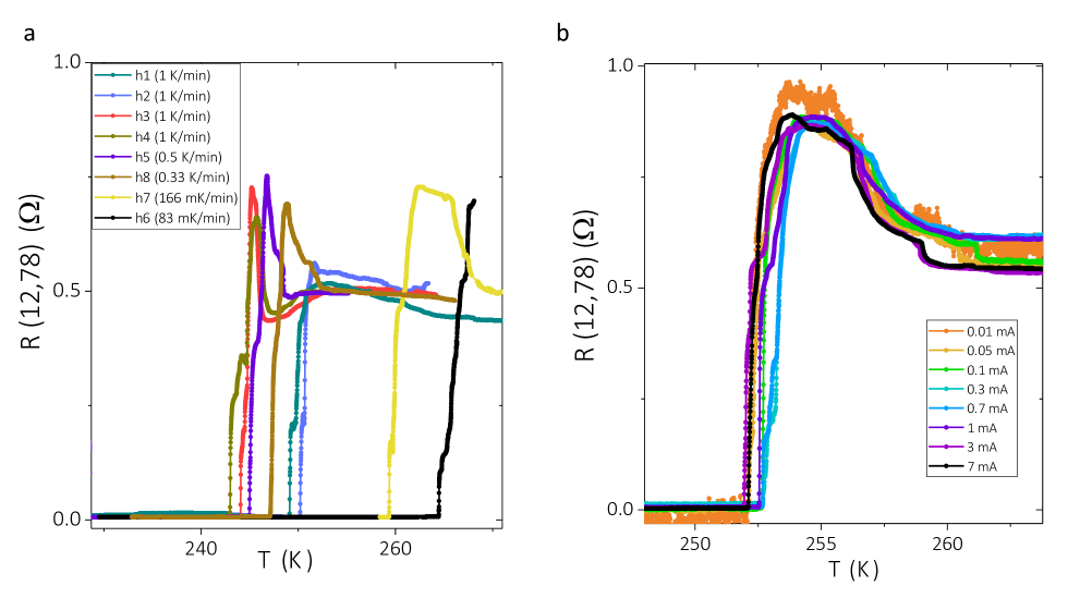
In order to investigate the thermal history and bias current dependence of excess resistance anomaly (ERA) in our Ag/Au nanostructures, we focus on the channel, which showed reasonably stable and reproducible behavior in multiple thermal cycles. In Fig. 2, we examined the behavior across the transition as a function of both rate of sweep (Fig. 2a) and biasing current (Fig. 2b). The data in Fig. 2a was taken at a constant bias current of mA for eight consecutive heating cycles at rate ranging from mK/min - K/min. The ERA evolves and eventually stabilizes with progressive thermal cycling with varying by K between the two successive thermal cycles for high sweep rates ( K/min). When the sweep rate is decreased, the ERA remains robust but the increases considerably, indicating the nanostructure film exists in an out-of-equilibrium state. Our earlier experiments thapa2018coexistence ; islam2019current indicated that in the Ag/Au nanostructures also change with ageing, which may complicate unambiguous determination of the effect of the sweep rate alone. A small ’dip’ in immediately following the peak, observed most clearly for cycles hh, has also been observed at the superconductor to normal transitions in Au0.7In0.3 rings wang2007observation and high- Bi2Sr2CaCu2O8-y films wan1993interlayer that associates the resistance anomaly to the fluctuation regime lindqvist1990new . In the eight subsequent thermal cycles (at sweep rate K/min), the biasing current was varied from A to 7 mA (Fig. 2b). The variation in K among these cycles is less than K, and ERA remains essentially unaffected in spite of nearly three decades of change in current. We note that although few experiments with patterned quasi-1D superconductors report suppression of excess resistance at large biasing current nordstrom1992resistance ; arutyunov1999resistive , several other investigations, for example those with the high- films mosqueira1994resistivity , suggest little or no effect of current density on the anomaly.
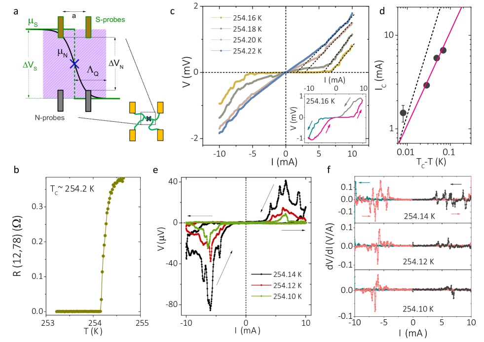
While there is no known analogue of the ERA in non-superconducting metallic nanostructure, the diversity of superconducting devices and materials that exhibit such a phenomenon has led to considerable debate in regard to its microscopic origin. An increase in resistivity in the vicinity of can arise from quasi-particle tunneling between the superconducting-normal (S-N) puddles in case of a granular superconductor rubin1992observation or vortex dynamics in the fluctuation regime francavilla1991observation ; harada2010large . Large excess resistance in granular doped nano-diamond films has been attributed to superconducting transition through an intermediate Bosonic insulating phase zhang2013metal . In case of out-of-line probe configuration, such as ours, Vaglio et al. showed that geometric redistribution of current in the presence spatially varying can provide a simple explanation of the resistance anomaly vaglio1993explanation . Non-equilibrium effect at the S-N boundary arutyunov1999resistive ; kwong1991interfacial and nucleation of interacting phase slip centers (PSC) park1995resistance ; park1997resistance have also been extensively discussed, particularly in the context of quasi-1D superconducting wires or filaments. In this latter case (see Fig. 3a), the qualitative understanding of the anomaly is based on the argument that when a PSC is formed in the current path and between the (superconducting) voltage leads, the supercurrent () is locally suppressed and the rest of the current is carried as quasi-particle current. The resulting voltage drop across a PSC is given by , where , and are the charge imbalance length, normal state resistivity and cross sectional area, respectively tinkham2004introduction . For lead separation , the nucleation of a PSC will cause a voltage drop that exceeds its normal state value when . When the bias current or temperature is increased, another PSC can nucleate in the close vicinity, but the ’effective repulsion’ between the PSCs, which now have to organize within a distance of , will shrink the extent of the charge-imbalance region . Thus the excess voltage is reduced, which also creates sequential non-monotonic features, and negative differential resistance (NDR) spikes, in the characteristics strunk1998resistance ; park1997resistance .
We note that the above model is valid under two crucial assumptions: (1) voltage-probe separation, and (2) voltage probes are superconducting. The validity of these two criteria may seem unlikely in the Ag/Au nanostructure films. However, recent investigation of the characteristics in these systems have indicated possible formation of PSCs at the resistive transition islam2019current , and attributed to a highly inhomogeneous and filamentary network of superconducting channels. Both resistance anisotropy and the strong spatial dependence of ratio (Fig. 1c inset) support this scenario. The microscopic superconducting filaments can form the voltage probes to the S-N interfaces in the current path in a fortuitous network pattern, and the condition of can be satisfied locally (schematic in Fig. 3a).
In order to explore the possibility of sequential excitation of PSCs in our case, we have investigated the 4-probe characteristics of the channel close to the resistive transition during cooling in a separate thermal cycle. The measurement consists of three ramping segments while cooling at mK/min: (i) ramping of current to mA, (ii) subsequently ramping up to mA, and (iii) finally decreasing down to mA. During each cycle, decreases by mK. Fig. 3c shows the increasing segment ( mA) of the characteristics at four temperatures across the transition. We first obtain the -dependence of from the four-probe voltage at mA in each cycle (Fig. 3b). From the thermally activated phase slip (TAPS) model islam2019current ; chu2004phase fit to the data, we obtain K in this cooling cycle. Notably, we do not observe a clear ERA in this cycle, possibly due to the indirect process followed to extract the data from characteristics.
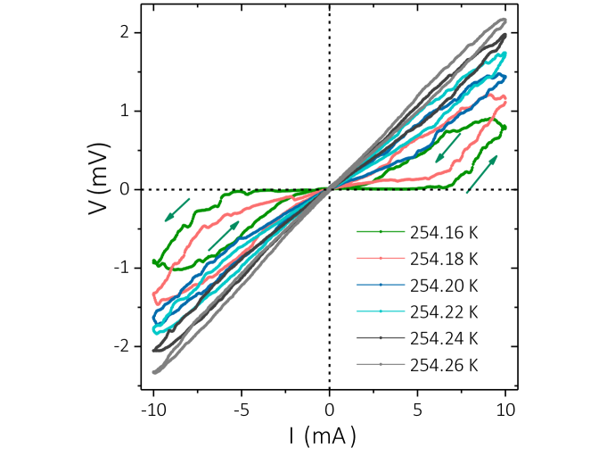
The characteristics in Fig. 3c clearly exhibit a -dependent critical current , symmetric in both directions, above which the voltage drop increases rapidly. We note: (1) As is lowered, the s becomes strongly hysteretic between the increasing and decreasing segments of (Inset of Fig. 3c, and supplementary information), as reported earlier in such films islam2019current . Such hysteresis is often observed in quasi-1D superconductors when driven above , and attributed to localized hot spots which involves Joule heating of dissipative centres like PSCs skocpol1974phase . (2) For , increases in small abrupt jumps which can be attributed to the sequential introduction of PSCs thereby a discontinuous change in the chemical potential. (3) Determining by extrapolating the high-current regime (dashed lines in Fig. 3c), we find that (Fig. 3d), which deviates from the expected dependence of (dotted line in Fig. 3d) in the Ginzburg-Landau theory tinkham2004introduction , but consistent with previous report on such films islam2019current .
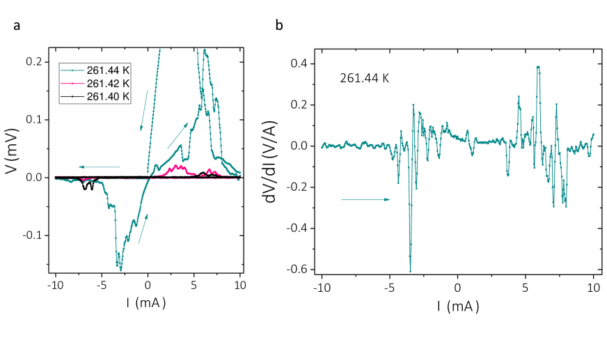
Intriguingly, when is lowered below mK from , the s exhibit a new feature as shown in Fig. 3e. While the increasing segment of current up to ( mA) remains mostly featureless, the four-probe exhibits sharp peaks as is reduced during the decreasing segment ( mA). The sharp peaks gradually disappear when is reduced mK below the . Similar sequence of peaks in characteristics were observed during controlled heating as well (See supplementary information). The positions of the peaks are nearly symmetric in regard to the direction of current ( mA etc.), although the peak voltage magnitude is not so, presumably due to the small temperature difference mK between the two ramping segments. The sequence of peaks in results in NDR as shown in Fig. 3f for three representative . The non-monotonic structures and NDR at zero and finite current/voltage bias has been observed for wide variety of superconducting systems and can arise from different mechanisms such as Coulomb blockade of Cooper-pair tunneling in Josephson-coupled junctions watanabe2001coulomb or interaction between the non-equilibrium regions around PSCs park1995resistance . The coherent tunneling of Cooper pairs in superconducting tunnel-junction is however a low temperature quantum effect and not necessarily confined to only the fluctuation regime near . Following the previous observation of excess voltage near , the interacting non-equilibrium regions across S-N interfaces or PSCs may be responsible for the sequence of peaks in and subsequently NDR in our Ag/Au nanostructure film. We note that the same is applicable for charge-imbalance regions with multiple S-N interfaces. The observation of these peaks only in the decreasing current segment is not fully understood (Fig. 3e), although we anticipate the likelihood of thermally activated nucleation of PSCs according to Langer-Ambegaokar-McCumber-Halperin (LAMH) mechanism langer1967intrinsic ; mccumber1970time , once the local hotspots are created by driving the current to a high value ( mA) during the increasing segment.
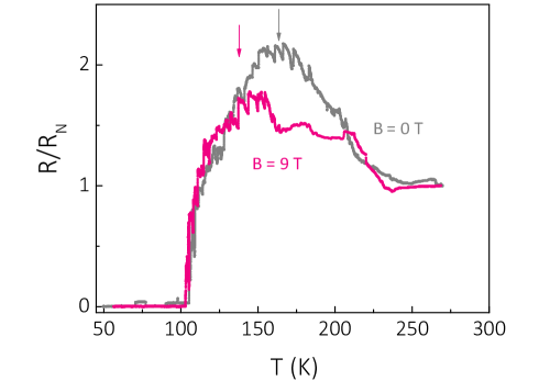
Finally, we discuss the effect of (perpendicular) magnetic field on the ERA using a Ag/Au nanostructure film, with lower K but a rather broad ( K) excess resistance region (Fig. 4), possibly due to greater level of inhomogeneity. We compare two cooling cycles of this film at fixed magnetic fields of zero and 9 Tesla. While the itself showed very little ( K) decrease at T, which is consistent with earlier suggestion of a short coherence length islam2019current , we observe (1) ratio is (partially) quenched in the presence of magnetic field at higher ( K), and (2) the maximum of shifts to lower (shown by the vertical arrows in Fig. 4). Both observations are consistent with the previous reports on effect of magnetic field on the excess resistance anomaly arutyunov1999resistive ; lindqvist1990new ; kwong1991interfacial ; crusellas1992giant . Within the charge imbalance model, the suppression of excess resistance at finite field is linked to the decrease in though orbital pair breaking and spin-flip scattering processes strunk1998resistance , whereas argument regarding negative magneto-resistance for the anomaly is based on the enhanced proximity effects that drives the charge-imbalance region away from the voltage probes kwong1991interfacial . However, other mechanisms such as interaction between the superconducting fluctuations and the conduction electrons lindqvist1990new ; gordon1986electron as well as the presence of collective modes in D superconducting filaments tidecks2006current can also reduce the resistance anomaly in the presence a magnetic field but these possibilities are probably unrelated to our observations in Ag/Au nano-structures.
In conclusion, we report the observation of resistance anomaly above the normal-state value in different regions of the Ag/Au nanostructure thin film near . The anomalous resistance persists over a range of bias currents and the thermal history of the sample. The characteristics exhibits critical current behavior, and current-driven sequential voltage peaks for , which manifests as negative differential resistances. Finally, we show that the resistance anomaly is partially quenched by the application of a perpendicular field of T. These observations serve as strong evidence of formation normal-superconductor interfaces in Ag/Au films at temperatures close to room temperature.
References
- (1) Berlincourt, T. G. Hall effect, resistivity, and magnetoresistivity of Th, U, Zr, Ti, and Nb. Phys. Rev. 114, 969 (1959).
- (2) Grassie, A. & Green, D. Transition anomalies of disordered aluminium films. Phys. Lett. A 31, 135–136 (1970).
- (3) Ems, S. & Swihart, J. Resistance peak at the superconducting transition of thin films of tin and indium. Phys. Lett. A 37, 255–256 (1971).
- (4) Tajima, Y. & Yamaya, K. Magnetic and electric field effects on the giant resistivity anomaly on the superconducting transition in TaSe3. J. Phys. Soc. Japan 53, 3307–3310 (1984).
- (5) Tajima, Y. & Yamaya, K. Giant resistivity anomaly on the superconducting transition in TaSe3. J. Phys. Soc. Japan 53, 495–498 (1984).
- (6) Yamamoto, H., Ikeda, M. & Tanaka, M. Giant resistivity anomaly in A15Nb3 (Ge, Si) superconductive films with compositionally modulated superstructure. Japanese J. Appl. Phys. 24, L314 (1985).
- (7) Lindqvist, P., Nordström, A. & Rapp, Ö. New resistance anomaly in the superconducting fluctuation region of disordered Cu-Zr alloys with dilute magnetic impurities. Phys. Rev. Lett. 64, 2941 (1990).
- (8) Crusellas, M., Fontcuberta, J. & Piñol, S. Giant resistive peak close to the superconducting transition in L2-xCexCuO4 single crystals. Phys. Rev. B 46, 14089 (1992).
- (9) Santhanam, P., Chi, C., Wind, S., Brady, M. & Bucchignano, J. Resistance anomaly near the superconducting transition temperature in short aluminum wires. Phys. Rev. Lett. 66, 2254 (1991).
- (10) Wan, Y., Hebboul, S., Harris, D. & Garland, J. Interlayer Josephson coupling of thermally excited vortices in Bi2Sr2CaCu2O8-y. Phys. Rev. Lett. 71, 157 (1993).
- (11) Vaglio, R., Attanasio, C., Maritato, L. & Ruosi, A. Explanation of the resistance-peak anomaly in nonhomogeneous superconductors. Phys. Rev. B 47, 15302 (1993).
- (12) Suzuki, M. Resistance peak at the resistive transition in high-Tc superconductors. Phys. Rev. B 50, 6360 (1994).
- (13) Moshchalkov, V., Gielen, L., Neuttiens, G., Van Haesendonck, C. & Bruynseraede, Y. Intrinsic resistance fluctuations in mesoscopic superconducting wires. Phys. Rev. B 49, 15412 (1994).
- (14) Mosqueira, J., Pomar, A., Diaz, A., Veira, J. & Vidal, F. Resistivity anomalies above the superconducting transition in Y1Ba2Cu3O7-δ crystals and non-uniformly distributed critical-temperature inhomogeneities. Phys. C: Superconductivity 225, 34–44 (1994).
- (15) Park, M., Isaacson, M. & Parpia, J. Resistance anomaly and excess voltage near superconducting interfaces. Phys. Rev. Lett. 75, 3740 (1995).
- (16) Silva, E., Lanucara, M. & Marcon, R. Microwave surface resistance peak at Tc in Bi2Sr2CaCu2O8+x film. Phys. C: Superconductivity 276, 84–90 (1997).
- (17) Park, M., Isaacson, M. & Parpia, J. Resistance anomaly and excess voltage in inhomogeneous superconducting aluminum thin films. Phys. Rev. B 55, 9067 (1997).
- (18) Strunk, C. et al. Resistance anomalies in superconducting mesoscopic Al structures. Phys. Rev. B 57, 10854 (1998).
- (19) Arutyunov, K. Y., Presnov, D., Lotkhov, S., Pavolotski, A. & Rinderer, L. Resistive-state anomaly in superconducting nanostructures. Phys. Rev. B 59, 6487 (1999).
- (20) Buzea, C., Tachiki, T., Nakajima, K. & Yamashita, T. The origin of resistance peak effect in high-temperature superconductors-apparent Tc anisotropy due to Jc anisotropy. IEEE Trans. Appl. Superconductivity 11, 3655–3658 (2001).
- (21) Wang, H., Rosario, M., Russell, H. & Liu, Y. Observation of double resistance anomalies and excessive resistance in mesoscopic superconducting Au0.7In0.3 rings with phase separation. Phys. Rev. B 75, 064509 (2007).
- (22) Harada, A. et al. Large energy dissipation due to vortex dynamics in mesoscopic Al disks. Phys. Rev. B 81, 174501 (2010).
- (23) Zhang, G., Zeleznik, M., Vanacken, J., May, P. W. & Moshchalkov, V. V. Metal–bosonic insulator–superconductor transition in boron-doped granular diamond. Phys. Rev. Lett. 110, 077001 (2013).
- (24) Thapa, D. K. et al. Coexistence of diamagnetism and vanishingly small electrical resistance at ambient temperature and pressure in nanostructures. arXiv preprint arXiv:1807.08572 (2018).
- (25) Islam, S. et al. Current-voltage characteristics in Ag/Au nanostructures at resistive transitions. arXiv preprint arXiv:1906.02291 (2019).
- (26) Urazhdin, S. Comment on arxiv: 1807.08572," coexistence of diamagnetism and vanishingly small electrical resistance at ambient temperature and pressure in nanostructures". arXiv preprint arXiv:1906.05742 (2019).
- (27) Pekker, D. & Levy, J. A comment on percolation and signatures of superconductivity in Au/Ag nanostructures. arXiv preprint arXiv:1808.05871 (2018).
- (28) Kwong, Y., Lin, K., Hakonen, P., Isaacson, M. & Parpia, J. Interfacial resistive anomaly at a normal-superconducting boundary. Phys. Rev. B 44, 462 (1991).
- (29) Thapa, D. K. et al. Unconventional optical response in engineered Au-Ag nanostructures. arXiv preprint arXiv:1906.05342 (2019).
- (30) Nordström, A. & Rapp, Ö. Resistance-peak anomaly in metallic glasses: Dependence on currents and contact arrangement. Phys. Rev. B 45, 12577 (1992).
- (31) Rubin, S., Schimpfke, T., Weitzel, B., Vossloh, C. & Micklitz, H. Observation of sharp resistance anomalies near Tc in granular superconductors. Annalen der Physik 504, 492–499 (1992).
- (32) Francavilla, T. & Hein, R. The observation of a transverse voltage at the superconducting transition of thin films. IEEE Trans. Magnetics 27, 1039–1042 (1991).
- (33) Tinkham, M. Introduction to superconductivity (Courier Corporation, 2004).
- (34) Chu, S. L., Bollinger, A. T. & Bezryadin, A. Phase slips in superconducting films with constrictions. Phys. Rev. B 70, 214506 (2004).
- (35) Skocpol, W., Beasley, M. & Tinkham, M. Phase-slip centers and nonequilibrium processes in superconducting tin microbridges. J. Low Temp. Phys. 16, 145–167 (1974).
- (36) Watanabe, M. & Haviland, D. B. Coulomb blockade and coherent single-Cooper-pair tunneling in single Josephson junctions. Phys. Rev. Lett. 86, 5120 (2001).
- (37) Langer, J. S. & Ambegaokar, V. Intrinsic resistive transition in narrow superconducting channels. Phys. Rev. 164, 498 (1967).
- (38) McCumber, D. & Halperin, B. Time scale of intrinsic resistive fluctuations in thin superconducting wires. Phys. Rev. B 1, 1054 (1970).
- (39) Gordon, J. M. & Goldman, A. M. Electron inelastic scattering in aluminum films and wires at temperatures near the superconducting transition. Phys. Rev. B 34, 1500 (1986).
- (40) Tidecks, R. Current-induced nonequilibrium phenomena in quasi-one-dimensional superconductors, vol. 121 (Springer, 2006).
.1 Supplementary Information