Magnetic polaron and antiferro-ferromagnetic transition in doped bilayer CrI3
Abstract
Gate-induced magnetic switching in bilayer CrI3 has opened new ways for the design of novel low-power magnetic memories based on van der Waals heterostructures. The proposed switching mechanism seems to be fully dominated by electrostatic doping. Here we explain, by first-principle calculations, the ferromagnetic transition in doped bilayer CrI3. For the case of a very small electron doping, our calculations predict the formation of magnetic polarons (“ferrons”, “fluctuons”) where the electron is self-locked in a ferromagnetic droplet in an antiferromagnetic insulating matrix. The self-trapping of holes is impossible, at least, within our approximation.
Introduction. The discovery of long-range ferromagnetic order in two-dimensional semiconductorsHuang et al. (2017); Gong et al. (2017); Deng et al. (2018); Gibertini et al. (2019) has opened new venues for the design and engineer of novel magneto-opticZhong et al. (2017); Seyler et al. (2018), magneto-electronicZollner et al. (2018); Song et al. (2018); Klein et al. (2018); Wang et al. (2018a); Cardoso et al. (2018); Ghazaryan et al. (2018); Wang et al. (2019); Rustagi et al. (2019) and spintronicKarpiak et al. (2019); Cummings (2019); Kim et al. (2019) devices based on van der Waals heterostructures. In chromium trihalides (CrX3), most of these applications rely on their layered-antiferromagnetic ground state, and on the low critical fields needed for a ferromagnetic phase transition (0.6-0.7 T and 1.1 T for bilayer CrI3 and CrCl3 respectively). Recent experiments by Thiel et al.Thiel et al. (2019) and Ubrig et al.Ubrig et al. (2019) have confirmed that the observed antiferromagnetic ground-state in CrI3 is related to the different layer stacking in bulk and few-layer samples. These experimental observations are in agreement with previous first-principles calculations predicting a strong reduction of interlayer exchange in bilayer CrI3 when going from rhombohedral to monoclinic stacking.Sivadas et al. (2018); Jiang et al. (2019); Jang et al. (2019); Soriano et al. (2019)
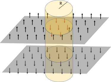
The low critical fields reported for bilayer CrI3 denote a weak interlayer exchange coupling able to be affected by other external perturbations. Recent experiments on dual-gated bilayer CrI3 have demonstrated that an electron doping of is able to switch the interlayer exchange coupling from antiferromagnetic(AFM) to ferromagnetic(FM)Jiang et al. (2018a). A similar behaviour has been reported for bilayer and few-layer CrI3 close to the interlayer spin-flip transitionJiang et al. (2018b); Huang et al. (2018), and also for Cr2Ge2Te3 samples,Wang et al. (2018b) thus allowing for a fully electrical control of interlayer magnetism in few-layer CrI3. A plausible mechanism describing magnetic transitions through electrostatic doping is based on the formation of magnetic polarons, as shown schematically in Fig.1, where a self-trapped electron is forming a local ferromagnetic environment of radius () in a bilayer antiferromagnetic system.
In this work, we shed some light on the mechanism underlying interlayer magnetic transition in electron/hole doped bilayer CrI3 by combining first-principles calculations and an effective low-energy model that allows us to describe the energy of the magnetic polaron in terms of the interlayer exchange coupling and the carrier bandwidth. In the first part, we perform ab-initio calculations in doped bilayer CrI3 and show the effect of electrostatic doping on the interlayer exchange coupling. In the second part, we introduce the effective model explaining qualitatively our numerical results via the formation of magnetic polarons in layered semiconducting magnets. In the last part, we discuss and summarize the results.
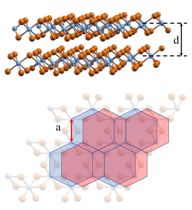
First-principles calculations. We have performed density functional theory (DFT+U) calculations on monoclinic bilayer CrI3 (see Fig.2) using the plane-wave based code PWscf as implemented in the Quantum-Espresso ab-initio packageGiannozzi et al. (2009). The Cr-Cr intralayer and interlayer distances obtained after relaxation are Å and Å. The quasi-Newton algorithm for ion relaxation is applied until the components of all forces are smaller than Ry. For the self consistent calculations, we use eV and a -point grid. Projector augmented wave (PAW) pseudopotentials within the Perdew-Burke-Ernzerhoff (PBE) approximationPerdew et al. (1996) for the exchange-correlation functional are used for Cr and I atoms. Van der Waals dipolar corrections are introduced through the semiempirical Grimme-D2 potential.Grimme (2006) Spin-orbit interactions are not included in our calculations.
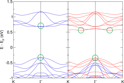
In Fig.3, we show the -centered band structure of monoclinic bilayer CrI3 for AFM and FM interlayer coupling. In the FM configuration, the strong hybridization of the empty Cr -orbitals localized on different layers modifies the dispersion of the conduction bands. This results in a lower and indirect bandgap in the FM case compared to the AFM one (green circles in Fig.3 indicate the top and bottom of conduction and valence bands). In the first two columns of Table 1, we show the energy values of the bottom(top) of conduction(valence) bands for AFM and FM interlayer coupling, as well as the calculated effective masses () for electron and hole carriers.
| VBMax (eV) | CBMin (eV) | |||
|---|---|---|---|---|
| AFM | -0.333 | 0.678 | 0.15 | 0.18 |
| FM | -0.339 | 0.555 | 0.02 | 0.11 |
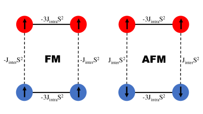
The calculation of the interlayer exchange coupling from first-principles calculations using a semiclassical approachLado and Fernández-Rossier (2017) entails several difficulties due to the complexity of the Cr-Cr interlayer hopping at the microscopic level.Soriano et al. (2019) Here, we adopt a simplified version by considering only a one-to-one Cr-Cr interlayer hopping (Fig.4). By doing so, we can write inter- and intralayer exchange couplings in terms of the total energies obtained using first-principles as:
| (1) |
where is the interlayer exchange energy, which depends on the electrostatic doping , is the intralayer exchange coupling, and is the total spin per Cr atom. In the ground state (), our first-principles calculations predict an interlayer AFM ground state with eV/Cr ( eV/Cr).
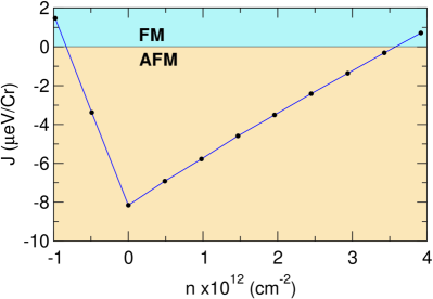
Now, we study the effect of electrostatic doping on the interlayer exchange coupling in bilayer CrI3 (). In Fig.5, we show the interlayer exchange coupling dependence on the electron and hole doping using first-principles calculations. The most interesting feature of this figure is the pronounce asymmetry around . The blue and yellow regions correspond to FM and AFM ground states. The doping needed to switch the interlayer magnetism is around 4 times higher for holes than for electrons, namely for the ferromagnetic transition. This has already been observed in a recent experiment by Huang et al.Huang et al. (2018)
Effective model. Let us now discuss qualitatively why doping transforms antiferromagnetic ordering into ferromagnetic. In general, a weak doping always favors ferromagnetism. Indeed, in ferromagnetic environment electron propagates with a given direction of spin with maximally possible hopping whereas in antiferromagnetic or paramagnetic cases it has to arrange its spin to the direction of localized magnetic moment which leads to effective narrowing of the gap and increases its average band energy, the mechanism known as double exchange Anderson (1963); Brinkman and Rice (1970); Auslender and Katsnelson (1982); Nagaev (1983). If the concentration of electrons is large enough, this ferromagnetic double exchange overcomes the initial antiferromagnetic exchange and the system turns into a ferromagnet, exactly as we see in our calculation. If the concentration of electrons is not high enough for this, the electron is supposed to form around itself a local ferromagnetic environment where it gets self-trapped, a phenomenon known as magnetic polaron, fluctuon, or ferron Nagaev (1983, 2001)Krivoglaz (1973a); *krivoglaz2Auslender and Katsnelson (1980a); *AK2Auslender and Katsnelson (1981, 2005, 2006). When the concentration of electrons or holes increases, the system is phase separated into ferromagnetic droplets containing all charge carriers within an antiferromagnetic insulating matrix. This phase separation was found numerically within the narrow-band Hubbard model by Visscher Visscher (1974); its formal theory was developed for the Hubbard and s-d exchange models at the Bethe lattice in Ref. Auslender and Katsnelson (1982).
Here, to have a physically transparent and quantitatively correct estimate, we will follow a simplified description of the magnetic polaron suggested by Mott Mott (1974). We will assume that the electron (or hole) is self-locked in a radially symmetric ferromagnetic region considering a potential well with impenetrable walls. We start with the fact that, according to our calculations, ferromagnetic ordering between the layers, in comparison with the antiferromagnetic one, shifts the bottom of the conduction band down and the top of the valence band up, which is the driving force of the magnetic polaron formation and electron self-localization.
The total energy of the magnetic polaron in a layered ferromagnetic material can be written as
| (2) |
where the first term is the carrier energy difference between parallel and anti-parallel interlayer magnetization, namely , where VB and CB stands for the top and bottom of valence and conduction bands respectively. The second term is the energy of a particle confined in a disc of radius (Fig.1), with being the first zero of the Bessel function . The third term is the exchange energy needed to switch the magnetic interaction between adjacent layers, where is the interlayer exchange coupling per magnetic atom, is the area occupied by a single Cr atom in the unit cell, and is the Cr-Cr intralayer distance.
Then, the ratio is given by
| (4) |
where is the effective carrier bandwidth. The model is applicable assuming that this ratio is much larger than one, which is necessary for the continuum-medium description adopted by us. As we will see further, this condition is satisfied in both our cases, for electrons and for holes.
Now, we rewrite Eq.1 in terms of the carrier energy difference (), the interlayer exchange coupling () and the carrier bandwidth () as
| (5) |
By using Eqs.4 and 5, together with the parameters obtained from first-principles calculations, we can study the feasibility of magnetic polaron formation in bilayer CrI3. First, we need to calculate the effective carrier bandwidths
| (6) |
where eV, Å is the Bohr atomic radius and is the free-electron mass. Using Eq.6, we obtain eV and eV for electrons and holes, respectively. Now, by applying Eq.4, we obtain and which is more than enough to justify our simplified continuous-medium description.
Finally, we calculate the ground state energy of the magnetic polaron for both carriers using Eq.5. From the first two columns of Table 1, we can calculate the energy difference for electron and hole carriers between the FM and AFM magnetic configurations, meV and meV. The total energies are meV and meV, which means that, within our approximation, the formation of a magnetic polaron with interlayer FM ordering in bilayer CrI3 is possible only for electrons.
In summary, we have predicted the formation of a magnetic polaron in electron-doped bilayer CrI3 using the parameters taken from first-principles calculations. These calculations also show that for electron doping the system transforms from the antiferromagnetic interlayer coupling to the ferromagnetic one. Our results give a possible explanation for the electrostatic interlayer magnetic switching experiments reported so far. It would be very interesting to study electron mobility for the case of very weakly doped system. For the case of electrons, it should be extremely small, due to electron self-trapping, and there should be a dramatic difference between electron- and hole-doped cases. The other prediction is that for the case of electron doping the atiferro-to-ferro transition should go via the intermediate two-phase region, whereas for the case of holes, due to the lack of magnetic polarons, there is no reason to expect this intermediate state
Acknowledgments. We acknowledge Efrén Navarro Moratalla and Malte Rösner for fruitful discussions. D.S. thanks financial support from EU through the MSCA project Nr. 796795 SOT-2DvdW. M.I.K. acknowledges finacial support by JTC-FLAGERA Project GRANSPORT.
References
- Huang et al. (2017) B. Huang, G. Clark, E. Navarro-Moratalla, D. R. Klein, R. Cheng, K. L. Seyler, D. Zhong, E. Schmidgall, M. A. McGuire, D. H. Cobden, W. Yao, D. Xiao, P. Jarillo-Herrero, and X. Xu, Nature 546, 270 (2017).
- Gong et al. (2017) C. Gong, L. Li, Z. Li, H. Ji, A. Stern, Y. Xia, T. Cao, W. Bao, C. Wang, Y. Wang, Z. Q. Qiu, R. J. Cava, S. G. Louie, J. Xia, and X. Zhang, Nature 546, 265 (2017).
- Deng et al. (2018) Y. Deng, Y. Yu, Y. Song, J. Zhang, N. Z. Wang, Z. Sun, Y. Yi, Y. Z. Wu, S. Wu, J. Zhu, J. Wang, X. H. Chen, and Y. Zhang, Nature 563, 94 (2018).
- Gibertini et al. (2019) M. Gibertini, M. Koperski, A. F. Morpurgo, and K. S. Novoselov, Nature Nanotechnology 14, 408 (2019).
- Zhong et al. (2017) D. Zhong, K. L. Seyler, X. Linpeng, R. Cheng, N. Sivadas, B. Huang, E. Schmidgall, T. Taniguchi, K. Watanabe, M. A. McGuire, W. Yao, D. Xiao, K.-M. C. Fu, and X. Xu, Science Advances 3, e1603113 (2017).
- Seyler et al. (2018) K. L. Seyler, D. Zhong, B. Huang, X. Linpeng, N. P. Wilson, T. Taniguchi, K. Watanabe, W. Yao, D. Xiao, M. A. McGuire, K.-M. C. Fu, and X. Xu, Nano Letters 18, 3823 (2018).
- Zollner et al. (2018) K. Zollner, M. Gmitra, and J. Fabian, New J. Phys. 20, 073007 (2018).
- Song et al. (2018) T. Song, X. Cai, M. W.-Y. Tu, X. Zhang, B. Huang, N. P. Wilson, K. L. Seyler, L. Zhu, T. Taniguchi, K. Watanabe, M. A. McGuire, D. H. Cobden, D. Xiao, W. Yao, and X. Xu, Science 360, 1214 (2018).
- Klein et al. (2018) D. R. Klein, D. MacNeill, J. L. Lado, D. Soriano, E. Navarro-Moratalla, K. Watanabe, T. Taniguchi, S. Manni, P. Canfield, J. Fernández-Rossier, and P. Jarillo-Herrero, Science 360, 1218 (2018).
- Wang et al. (2018a) Z. Wang, I. Gutiérrez-Lezama, N. Ubrig, M. Kroner, M. Gibertini, T. Taniguchi, K. Watanabe, A. Imamoğlu, E. Giannini, and A. F. Morpurgo, Nature Communications 9, 2516 (2018a).
- Cardoso et al. (2018) C. Cardoso, D. Soriano, N. A. García-Martínez, and J. Fernández-Rossier, Phys. Rev. Lett. 121, 067701 (2018).
- Ghazaryan et al. (2018) D. Ghazaryan, M. T. Greenaway, Z. Wang, V. H. Guarochico-Moreira, I. J. Vera-Marun, J. Yin, Y. Liao, S. V. Morozov, O. Kristanovski, A. I. Lichtenstein, M. I. Katsnelson, F. Withers, A. Mishchenko, L. Eaves, A. K. Geim, K. S. Novoselov, and A. Misra, Nature Electronics 1, 344 (2018).
- Wang et al. (2019) Z. Wang, M. Gibertini, D. Dumcenco, T. Taniguchi, K. Watanabe, E. Giannini, and A. F. Morpurgo, Nature Nanotechnology 14, 1116 (2019).
- Rustagi et al. (2019) A. Rustagi, A. Solanki, Y. Tserkovnyak, and P. Upadhyaya, arXiv e-prints (2019).
- Karpiak et al. (2019) B. Karpiak, A. W. Cummings, K. Zollner, M. Vila, D. Khokhriakov, A. M. Hoque, A. Dankert, P. Svedlindh, J. Fabian, S. Roche, and S. P. Dash, arXiv e-prints , arXiv:1908.05524 (2019), arXiv:1908.05524 [cond-mat.mes-hall] .
- Cummings (2019) A. W. Cummings, J. Phys. Mater. 2, 045007 (2019).
- Kim et al. (2019) M. Kim, P. Kumaravadivel, J. Birkbeck, W. Kuang, S. G. Xu, D. G. Hopkinson, J. Knolle, P. A. McClarty, A. I. Berdyugin, M. Ben Shalom, R. V. Gorbachev, S. J. Haigh, S. Liu, J. H. Edgar, K. S. Novoselov, I. V. Grigorieva, and A. K. Geim, Nature Electronics 2, 457 (2019).
- Thiel et al. (2019) L. Thiel, Z. Wang, M. A. Tschudin, D. Rohner, I. Gutiérrez-Lezama, N. Ubrig, M. Gibertini, E. Giannini, A. F. Morpurgo, and P. Maletinsky, Science (2019).
- Ubrig et al. (2019) N. Ubrig, Z. Wang, J. Teyssier, T. Taniguchi, K. Watanabe, E. Giannini, A. F. Morpurgo, and M. Gibertini, arXiv e-prints , arXiv:1908.09607 (2019), arXiv:1908.09607 [cond-mat.mes-hall] .
- Sivadas et al. (2018) N. Sivadas, S. Okamoto, X. Xu, C. J. Fennie, and D. Xiao, Nano Letters 18, 7658 (2018).
- Jiang et al. (2019) P. Jiang, C. Wang, D. Chen, Z. Zhong, Z. Yuan, Z.-Y. Lu, and W. Ji, Phys. Rev. B 99, 144401 (2019).
- Jang et al. (2019) S. W. Jang, M. Y. Jeong, H. Yoon, S. Ryee, and M. J. Han, Phys. Rev. Materials 3, 031001 (2019).
- Soriano et al. (2019) D. Soriano, C. Cardoso, and J. Fernández-Rossier, Solid State Communications 299, 113662 (2019).
- Jiang et al. (2018a) S. Jiang, L. Li, Z. Wang, K. F. Mak, and J. Shan, Nature Nanotechnology 13, 549 (2018a).
- Jiang et al. (2018b) S. Jiang, J. Shan, and K. F. Mak, Nature Materials 17, 406 (2018b).
- Huang et al. (2018) B. Huang, G. Clark, D. R. Klein, D. MacNeill, E. Navarro-Moratalla, K. L. Seyler, N. Wilson, M. A. McGuire, D. H. Cobden, D. Xiao, W. Yao, P. Jarillo-Herrero, and X. Xu, Nature Nanotechnology 13, 544 (2018).
- Wang et al. (2018b) Z. Wang, T. Zhang, M. Ding, B. Dong, Y. Li, M. Chen, X. Li, J. Huang, H. Wang, X. Zhao, Y. Li, D. Li, C. Jia, L. Sun, H. Guo, Y. Ye, D. Sun, Y. Chen, T. Yang, J. Zhang, S. Ono, Z. Han, and Z. Zhang, Nature Nanotechnology 13, 554 (2018b).
- Giannozzi et al. (2009) P. Giannozzi, S. Baroni, N. Bonini, M. Calandra, R. Car, C. Cavazzoni, D. Ceresoli, G. L. Chiarotti, M. Cococcioni, I. Dabo, A. D. Corso, S. de Gironcoli, S. Fabris, G. Fratesi, R. Gebauer, U. Gerstmann, C. Gougoussis, A. Kokalj, M. Lazzeri, L. Martin-Samos, N. Marzari, F. Mauri, R. Mazzarello, S. Paolini, A. Pasquarello, L. Paulatto, C. Sbraccia, S. Scandolo, G. Sclauzero, A. P. Seitsonen, A. Smogunov, P. Umari, and R. M. Wentzcovitch, Journal of Physics: Condensed Matter 21, 395502 (2009).
- Perdew et al. (1996) J. P. Perdew, K. Burke, and M. Ernzerhof, Physical review letters 77, 3865 (1996).
- Grimme (2006) S. Grimme, Journal of computational chemistry 27, 1787 (2006).
- Lado and Fernández-Rossier (2017) J. L. Lado and J. Fernández-Rossier, 2D Materials 4, 035002 (2017).
- Anderson (1963) P. W. Anderson, Solid State Physics, Vol. 14 (Academic Press, N. Y., 1963) p. 99.
- Brinkman and Rice (1970) W. F. Brinkman and T. M. Rice, Phys. Rev. B 2, 1324 (1970).
- Auslender and Katsnelson (1982) M. I. Auslender and M. I. Katsnelson, Solid State Commun. 44, 387 (1982).
- Nagaev (1983) E. L. Nagaev, Physics of magnetic semiconductors (Mir - Moscow, 1983).
- Nagaev (2001) E. L. Nagaev, Phys. Rep. 346, 388 (2001).
- Krivoglaz (1973a) M. A. Krivoglaz, Uspekhi Fiz. Nauk 111, 261 (1973a).
- Krivoglaz (1973b) M. A. Krivoglaz, Engl. Transl.: Sov. Phys. Uspekhi 16, 856 (1973b).
- Auslender and Katsnelson (1980a) M. I. Auslender and M. I. Katsnelson, Teor. Matem. Fizika 43, 261 (1980a).
- Auslender and Katsnelson (1980b) M. I. Auslender and M. I. Katsnelson, Engl. Transl.: Theor. Math. Phys. 43, 450 (1980b).
- Auslender and Katsnelson (1981) M. I. Auslender and M. I. Katsnelson, J. Magn. Magn. Mater. 241, 117 (1981).
- Auslender and Katsnelson (2005) M. I. Auslender and M. I. Katsnelson, Phys. Rev. B 72, 113107 (2005).
- Auslender and Katsnelson (2006) M. I. Auslender and M. I. Katsnelson, Ann. Phys. (N. Y.) 321, 1762 (2006).
- Visscher (1974) P. B. Visscher, Phys. Rev. B 10, 843 (1974).
- Mott (1974) N. F. Mott, Metal-Insulator Transitions (Taylor and Francis, London, 1974).