Spin splitting and strain in epitaxial monolayer WSe2 on graphene
Abstract
We present the electronic and structural properties of monolayer WSe2 grown by pulsed-laser deposition on monolayer graphene (MLG) on SiC. The spin splitting in the WSe2 valence band at was eV by angle-resolved photoemission spectroscopy (ARPES). Synchrotron-based grazing-incidence in-plane X-ray diffraction (XRD) revealed the in-plane lattice constant of monolayer WSe2 to be . This indicates a lattice compression of 0.19% from bulk WSe2. By using experimentally determined graphene lattice constant (), we found that a 33 unit cell of the slightly compressed WSe2 is perfectly commensurate with a 44 graphene lattice with a mismatch below 0.03%, which could explain why the monolayer WSe2 is compressed on MLG. From XRD and first-principles calculations, however, we conclude that the observed size of strain is negligibly small to account for a discrepancy in found between exfoliated and epitaxial monolayers in earlier ARPES. In addition, angle-resolved, ultraviolet and X-ray photoelectron spectroscopy shed light on the band alignment between WSe2 and MLG/SiC and indicate electron transfer from graphene to the WSe2 monolayer. As further revealed by atomic force microscopy, the WSe2 island size depends on the number of carbon layers on top of the SiC substrate. This suggests that the epitaxy of WSe2 favors the weak van der Waals interactions with graphene while it is perturbed by the influence of the SiC substrate and its carbon buffer layer.
I Introduction
Two-dimensional (2D) transition metal dichalcogenides (TMDs) MX2 (M = Mo or W, X= S, Se, or Te) possess outstanding electronic, spin, and optical properties at thicknesses of a few layers and hold great promise for future optoelectronic and spintronic applications Mak2016 ; Rivera2018 ; Wang2018 ; Mak2018 ; Wang2012 ; Novoselov2016 . In the monolayer limit, the breaking of structural inversion symmetry gives rise to a large spin splitting in the top valence band located at the and points of the surface Brillouin zone Xiao2012 ; Zhu2011 ; Yuan2013 . Due to time reversal symmetry, the and valleys have opposite out-of-plane spin polarization and each valley is associated with optical selection rules of opposite chirality as well as opposite signs of Berry curvature Xiao2012 . This leads to the valley-contrasting physics of monolayer TMDs, such as optical valley polarization and the valley Hall effect Mak2016 ; Mak2018 . Recent advances in the application of TMDs as a quantum light source is remarkable, especially for WSe2 Srivastava2015 ; He2015 ; Koperski2015 ; Chakraborty2015 ; Luo2018 ; Lu2019 , where the spin-valley degree of freedom is found to be robust also in local bound carriers Lu2019 .
The spin splitting in the valence band at is revealed directly by angle-resolved photoemission spectroscopy (ARPES) Zhang2013 ; Chiu2014 ; Eknapakul2014 ; Riley2014 ; Le2015 ; Zhang2016 ; Aretouli2015 ; Diaz2015 ; Latzke2015 ; Riley2015 ; Sugawara2015 ; Aretouli2016 ; Mo2016 ; Aziza2017 ; Forti2017 ; Henck2017 ; Agnoli2018 ; Wilson2017 . Spin-resolved ARPES confirmed an out-of-plane spin polarization that disappears for an even number of layers, consistent with the idea that inversion asymmetry is essential for the spin splitting Mo2016 . As demonstrated by theory and experiment, WSe2 has the largest spin splitting amongst all TMDs of 2H-type Xiao2012 ; Zhu2011 ; Le2015 ; Zhang2016 ; Wilson2017 . Le et al. reported meV in monolayer WSe2 exfoliated from a bulk crystal Le2015 , while very recent work on an exfoliated monolayer WSe2 reported meV Nguyen2019 . Zhang et al. found meV in monolayer WSe2 grown by molecular beam epitaxy (MBE) on bilayer graphene/SiC Zhang2016 . The discrepancy in between the MBE-grown and earlier exfoliated monolayer has been attributed to potential strain in the epitaxial TMD layer Zhang2016 . However, an evaluation of such strain in monolayer WSe2 using a precise structural probe, such as X-ray diffraction, has thus far been missing in any of the ARPES-studied monolayer.
Besides inducing strain, the substrate beneath a TMD could have an effect on its electronic properties by affecting the growth mode or via charge redistribution at the interface Sun2017 . TMDs on graphene represent a prototypical van der Waals (vdW) heterostructure where charge transfer could critically influence the physical properties of the TMD Froehlicher2018 . In this regard, ARPES of the graphene -bands before and after the creation of a vdW heterostructure could provide a direct evidence of charge transfer across the TMD/graphene interface, but no such experiment has yet been reported. Alternatively, the charge transfer can be indirectly assessed from the position of the valence band maximum of the TMD () with respect to the Fermi level . In WS2 grown by chemical vapor deposition on epitaxial monolayer graphene on SiC, Forti et al. found eV Forti2017 . Taking into account a band gap of 2.1 eV for pristine monolayer WS2, where is assumed to lie mid-gap, this corresponds to a significant downshift of eV of the WS2 bands. This, in turn, indicates electron transfer to WS2 across the interface. For MBE-grown WSe2 on epitaxial bilayer graphene, ARPES and scanning tunneling spectroscopy (STS) yielded eV Zhang2016 . Considering a band gap of 1.95 eV as determined by STS, this also suggests a small downshift ( meV) of the WSe2 bands, consistent with an electron transfer to the TMD layer. On the other hand, ARPES of monolayer WSe2 transferred to cleaved graphite yielded eV Wilson2017 . Assuming the same band gap , this corresponds to residing closer to the valence band and thus indicates a hole transfer to WSe2. However, we note that the above results are only indirect indications of charge transfer, because the position of the Fermi level can depend on the way the respective heterostructure was prepared. To unambiguously resolve the issue of charge transfer across the TMD/graphene interface, a comparison of ARPES measurements performed both before and after the creation of the vdW heterostructure could be highly useful.
In this paper, we clarify the electronic structure of monolayer WSe2 grown by pulsed-laser deposition on epitaxial monolayer graphene on SiC (MLG/SiC). In particular, we address the issue of a potential strain effect on the spin splitting by using ARPES and grazing-incidence X-ray diffraction (GIXRD) data, supported by an analysis based on first-principles calculations. The electron transfer from graphene to WSe2 is revealed by comparing ARPES of the graphene -bands before and after the WSe2 deposition. Ultraviolet and X-ray photoelectron spectroscopy (UPS and XPS), which are also conducted before and after the WSe2 growth, shed light on the band alignment between monolayer WSe2 and graphene. Atomic force microscopy (AFM) further reveals a significant impact of the substrate morphology on the WSe2 island size.
II Experiment and theory
Monolayer graphene (MLG) on SiC was grown using the well-established recipe of sublimation growth at elevated temperatures in argon atmosphere Emtsev2009 ; Forti2014 . Note that, on SiC, the graphene monolayer resides on top of a -reconstructed carbon buffer layer (zerolayer graphene, ZLG) that is covalently bound to the SiC substrate Riedl2010 . WSe2 films were grown on the thus prepared MLG/SiC substrates via hybrid-pulsed-laser deposition (h-PLD) in ultra-high vacuum (UHV) Avaise . This recently developed, bottom-up technique utilizes a pulsed laser to ablate transition metal targets, supported by chalcogen vapor supplied from an effusion cell, thus combining PLD and MBE. Pure tungsten (99.99 %) was ablated using a pulsed KrF excimer laser (248 nm) with a repetition rate of 10 Hz, while pure selenium (99.999 %) was evaporated from a Knudsen cell at a flux rate of around 1.5 Å/s as monitored by a quartz crystal microbalance. The deposition was carried out at 450 ∘C for three hours, followed by two-step annealing at 640 ∘C and 400 ∘C for one hour each. Further details on h-PLD can be found elsewhere Avaise . GIXRD measurements were carried out at the I07 beamline of Diamond Light Source Nicklin2016 , with a photon energy of 12 keV (wavelength 1.0332 Å) and a Pilatus 100K 2D detector (DECTRIS). The incident angle of the X-rays was chosen according to the critical angle of the samples, which were kept in helium atmosphere during the measurements. Topographic AFM images were acquired with a Bruker microscope in peak force tapping mode. For photoelectron spectroscopy and LEED measurements, the freshly prepared samples were capped with a 10 nm-thick selenium layer at room temperature and transported through air into a different UHV facility, where the capping layer was removed by heating to 300 ∘C. ARPES and UPS measurements were performed using monochromatized HeI (21.22 eV) and HeII (40.81 eV) photons and a 2D hemispherical analyzer equipped with a CCD Detector (SPECS Phoibos 150). The energy resolution of ARPES analyzer was 60 or 90 meV at a pass energy of 20 or 30 eV, respectively, as measured from the Fermi edge of gold at room temperature. XPS was carried out using non-monochromatized Mg K (1253.6 eV) radiation. All the measurements took place at room temperature. First-principles calculations were performed using density functional theory (DFT) as implemented in WIEN2k wien2k and ADF-BAND ADF-BAND ; BAND . The generalized gradient approximation as parameterized by Perdew-Burke-Ernzerhof PBE was used to describe the exchange-correlation functional. The spin-orbit coupling is included in a second variational procedure (Wien2k) or in the original basis set (ADF-BAND). We used a -point mesh of 16161 and adopted a slab geometry with a 30 Å gap between adjacent layers to suppress the interlayer interaction.
III Results and discussion
III.1 Electronic structure and strain
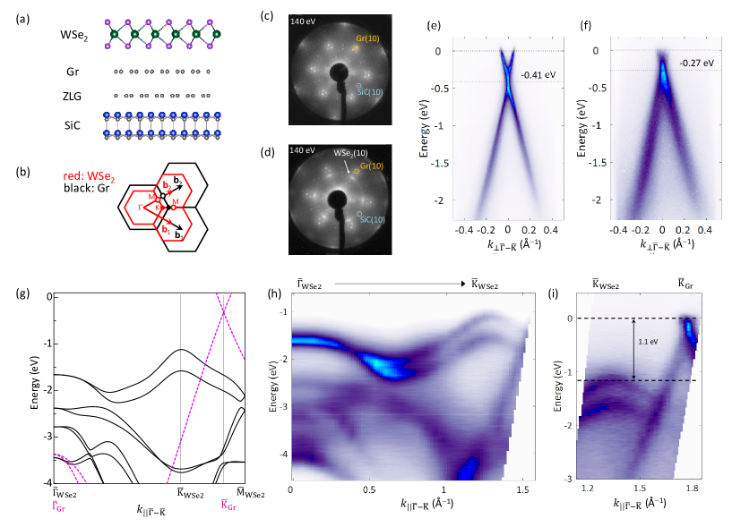
The vertical structure of the WSe2/MLG heterostack is schematically shown in Fig. 1(a). Figures 1(c) and (d) show the LEED patterns obtained before and after the growth of monolayer WSe2 on MLG/SiC with a coverage of approximately 50 %, demonstrating the preferred epitaxial relationship between WSe2 and graphene (WSe2 [] graphene []). This epitaxial relationship of the vdW heterostructure results in a reciprocal space alignment as shown in Fig. 1(b). The APRES intensity map recorded along the direction of WSe2 and graphene is shown in Fig. 1(h). The valence bands of monolayer WSe2 are resolved with excellent quality, essentially consistent with the result of the first-principles calculation [see Fig. 1(g)]. As expected from the reciprocal space alignment, the graphene -bands with their characteristic linear dispersion in the vicinity of the Fermi level also appear at higher parallel momenta [see Figs. 1(h) and (i)]. Note that the -bands are shifted in energy before and after the WSe2 deposition as revealed by the corresponding energy-momentum cuts recorded at the graphene point perpendicular to the direction [see Figs. 1(e) and (f)]. Before the WSe2 deposition, the Dirac point is found 0.41 eV below , reflecting the -type doping of epitaxial graphene on SiC Riedl2010 . After the growth of WSe2 on top of graphene, the Dirac point has shifted to 0.27 eV below . This upshift of 140 meV indicates electron transfer from graphene to the TMD monolayer which will be further discussed in Sec. III.2.
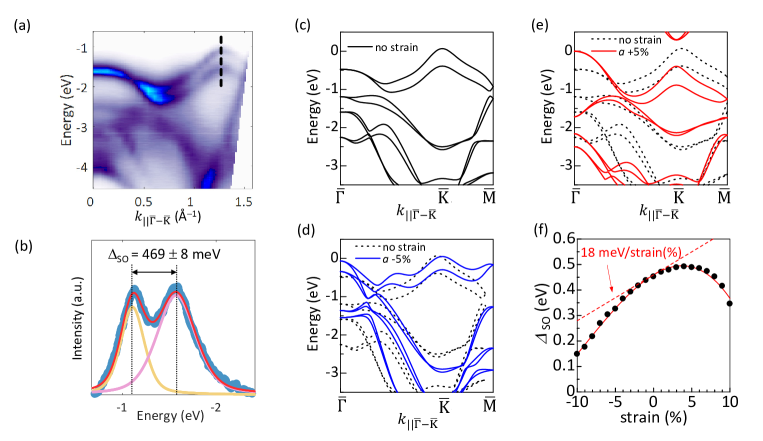
The large spin splitting arising in the topmost WSe2 valence band at due to the breaking of inversion symmetry in monolayer WSe2 is clearly resolved in the ARPES data [see Figs. 1(h), (i) and 2(a), (b)]. To quantify this splitting, an energy distribution curve (EDC) was extracted at the point of WSe2 as indicated by the dashed black line in Fig. 2(a). By fitting this EDC with two pseudo-Voigt curves as shown in Fig. 2(b), we obtain eV. The detail of the EDC analysis is shown in Supplemental Material SM . This value is appreciably smaller than the 513 meV observed in monolayer WSe2 exfoliated from a bulk crystal Le2015 , while close to more recent recent result (485 meV) Nguyen2019 and MBE-grown WSe2 (475 meV) Zhang2016 . While it is tempting to relate this difference to strain resulting from the epitaxial TMD growth, we will show in the following that the influence of strain on is actually negligible for WSe2 on graphene.
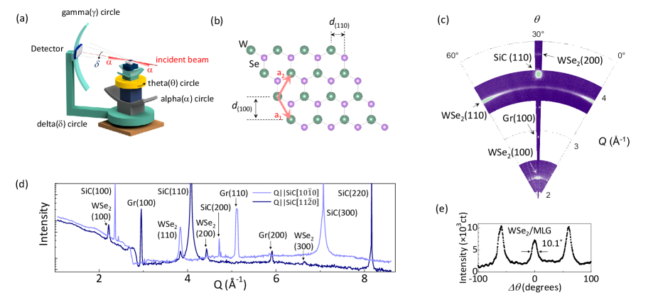
We first focus on the results obtained from synchrotron-based GIXRD Avaise . Utilizing an X-ray beam that propagates parallel to the sample surface at a critical angle of incidence [see Fig. 3(a)], this technique probes the in-plane structure of the WSe2 films [see Fig. 3(b)]. The in-plane reciprocal space map shown in Fig. 3(c) clearly captures diffraction from monolayer WSe2. We find WSe2 [] graphene [], fully consistent with LEED [see Fig. 1(d)]. The weak ring-like elongation of the WSe2 diffraction in the reciprocal space map reflects large crystalline mosaic of monolayer WSe2 islands with respect to rotation around the surface normal. The wide-angle () rocking () scan for the WSe2(110) peak exhibits the expected periodicity of as shown in Fig. 3(e). To evaluate the potential strain in the epitaxial TMD film, the in-plane lattice constant of WSe2 was extracted from the - scans shown in Fig. 3(d). We find , which indicates a small compression of % with respect to the bulk reference value ( Schutte ). The detail of the extraction of lattice constant and error is shown in the Supplemental MaterialSM . The lattice constant of MLG directly beneath WSe2 is determined to be from the same - scans. Using these values, we deduce that on MLG/SiC, a 33 unit cell of the compressed WSe2 is perfectly commensurate with a 44 graphene lattice, with an experimentally determined mismatch below 0.03 %. This could explain why monolayer WSe2 is compressed on MLG.
We now turn to the result of the first-principles calculation to examine the role of strain. Figures 2(c-f) show how a compressive or tensile strain modifies the valence band structure of monolayer WSe2. In the respective calculations, the in-plane lattice constant was changed proportionally to include strain while keeping the unit cell volume constant. Qualitatively, our calculations indicate that compressive strain reduces the value of [Fig. 2(f)], which is in accordance with previous first-principles results Le2015 . We find = 452 (475) meV using Wien2k (ADF-BAND) for “zero strain”, i.e., when we fix the lattice constants of monolayer identical to bulk. By introducing strain, inferred change in is () 18 meV per 1 % of tensile (compressive) strain as shown in Fig. 2(f). This holds for moderately strained WSe2 (as is the case in experiment) while the general dependence of on strain is clearly nonlinear. Using the experimentally determined value of the lattice compression of WSe2 on graphene (0.19 %), the amount of change in that could arise from compressed strain is 3.4 meV. This is smaller than the error in experimental (4698 meV), and much smaller than the difference of 44 meV between our epitaxial monolayer WSe2 and the exfoliated one from a bulk crystal Le2015 . We thus conclude that a strain effect cannot explain the discrepancy in .
A subtle issue in the approach we used to estimate strain is that we actually do not know the lattice constant of a freestanding monolayer WSe2. Namely, a monolayer WSe2 even without substrate effects may not have an identical lattice constant as that of bulk counterpart. To examine this, we performed additional first-principles calculations for bulk and monolayer WSe2 with structural optimizationSM . The theoretical results showed that the lattice constant of monolayer WSe2 converges to almost identical value as that of bulk (expanded only by 0.03% SM ). This means that the experimentally observed compression (0.19%) could be attributed to a strain in monolayer WSe2 as we have assumed.
Because strain in the epitaxial WSe2 is excluded as an origin of discrepancy in , we point out alternative possibilities. We first examined the possibility that the larger observed in exfoliated WSe2 came from a tensile strain in the flake when transferred to the substrate. By using the second-order polynomial fit to the vs. strain plot [Fig. 2(f)], we found the maximum gain in predicted by the theory is meV for % tensile strain. This is close to the experimentally found difference (48 meV), which means that 4-5% of tensile strain in the exfoliated bulk is needed to reproduce the value observed in the exfoliated bulk by strain. However, this is unlikely because the band dispersion of monolayer WSe2 expected for such a large strain [see Fig. 2(e)], which is rather different from the pristine monolayer, is not observed in the ARPES of the exfoliated bulk Le2015 . A very recent ARPES on exfoliated WSe2 by Nguyen et al. Nguyen2019 showed that (i) =0.4850.01 eV for monolayer, much closer to the value observed in this study, and (ii) =0.5010.01 eV for bilayer WSe2, which is close to that of earlier exfoliated monolayer result Le2015 . Thus, a more plausible origin for discrepancy may be that the larger in the previous study was obtained due to some inclusion of bilayer WSe2 in an exfoliated monolayer.
III.2 Band alignment and charge transfer
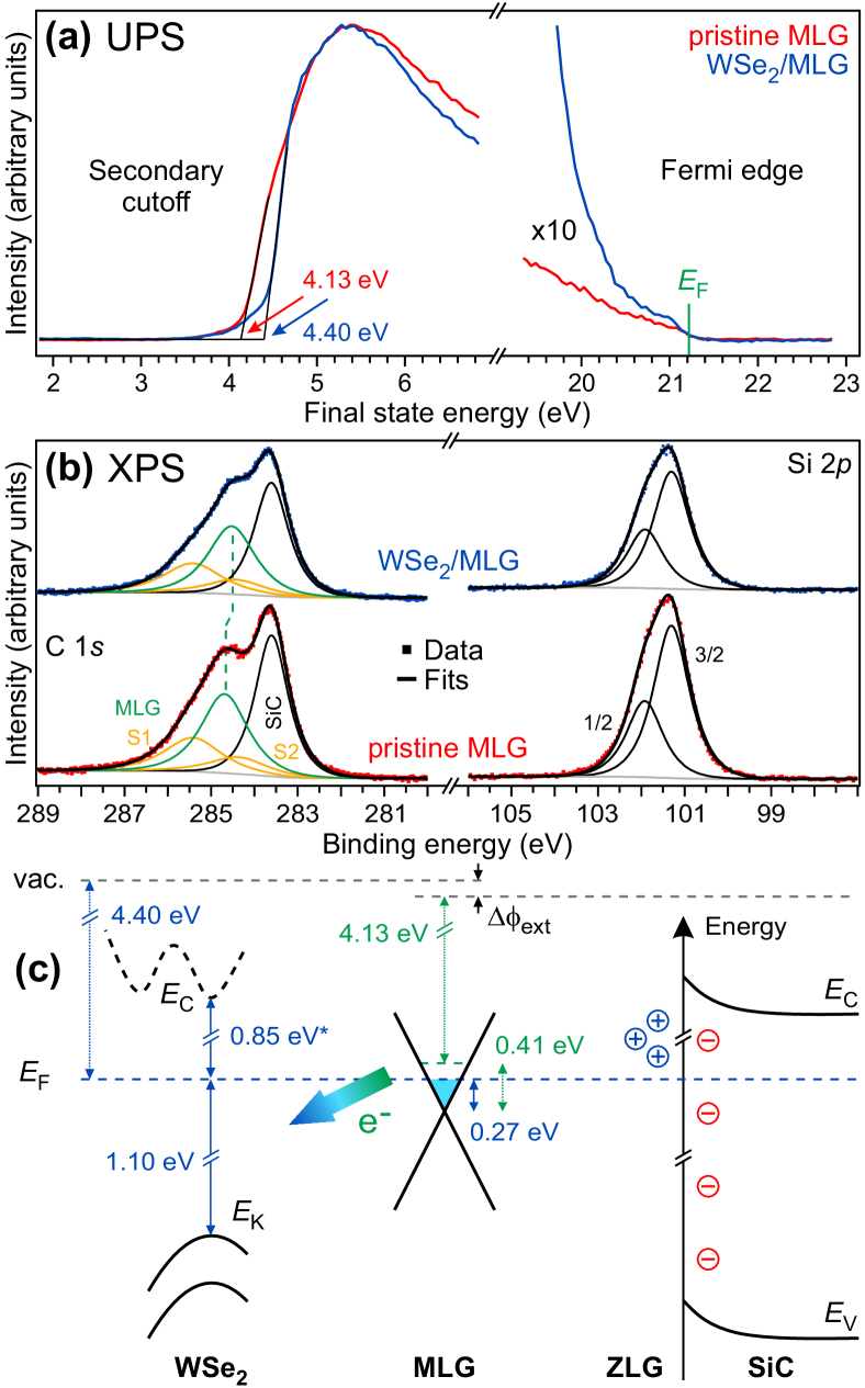
The sample work function can be measured using UPS. From the secondary cutoffs of the respective spectra as shown in Fig. 4(a), we infer eV and 4.40 eV ( eV) before and after the growth of WSe2, respectively. In combination with the ARPES results of Sec. III.1, we derive the band alignment of the WSe2/MLG heterostructure as sketched in Fig. 4(c). In quasi-free standing graphene, the bulk polarization of the SiC substrate induces an upward band bending, which would result in -doping of the surface when terminated by a clean interface Ristein2012 . Yet, with the presence of the buffer layer (ZLG) this is overcompensated by donor states at the graphene/SiC interface, resulting in the -type character of epitaxial MLG/SiC Mammadov2017 with its Dirac point residing 0.41 eV below [see Fig. 1(e)]. As discussed in Sec. III.1, the Dirac point shifts up by 0.14 eV to 0.27 eV below upon WSe2 growth [see Fig. 1(f)]. To our knowledge, such a shift of the graphene -bands upon TMD growth on top was not reported previously. There are two possible mechanisms to explain this observation. First, electron transfer from graphene to WSe2 could shift the graphene bands upwards. Second, if the donor states at the graphene/SiC interface are partially compensated during the TMD growth (e.g. via chemical reaction with the Se vapor), the amount of -type doping of graphene could change. In the latter case, modified donor states should influence the band bending at the graphene/SiC interface, which can be detected via a shift of the SiC core levels. The fitted XPS core level spectra of C and Si are shown in Fig. 4(b). The C fits consist of four components representing bulk SiC, MLG and the carbon buffer layer with its partial bonding to SiC (S1 and S2) Riedl2010 . The Si spectra can reasonably well be fitted by one spin-orbit split doublet ( and with an area ratio of 2:1). We find that the SiC peaks are unshifted in energy after the growth of WSe2, indicating that the band bending at the interface remains unchanged. From this, we can exclude that the reduced -type doping of graphene results from a modification of the interfacial donor states during TMD growth. Upon WSe2 growth the C MLG component shifts by eV to lower binding energies while S1 and S2 retain their positions. This core level shift of MLG is quantitatively in line with the upshift of the Dirac point observed in ARPES and further supports the scenario of electron transfer from MLG to WSe2. The work function increases by the charge transfer, and we ascribe the remaining increase of eV to an extrinsic upshift of the vacuum level due to the change in surface termination from MLG to WSe2[Fig. 4(c)]. The valence band maximum of WSe2 is found eV below in our ARPES measurements [see Fig. 1(i)], which matches very well with the results obtained from MBE-grown epitaxial WSe2 on bilayer graphene Zhang2016 . By assuming a band gap of eV as previously determined by STS Zhang2016 , we estimate that the conduction band minimum is located eV above . As such, the Fermi level in WSe2 resides closer to the conduction band minimum than to the valence band maximum. We finally note that a finite density of in-gap states can be expected in our epitaxial WSe2 films, stabilizing the position of inside the band gap after the electron transfer from graphene.
III.3 Morphology of monolayer WSe2
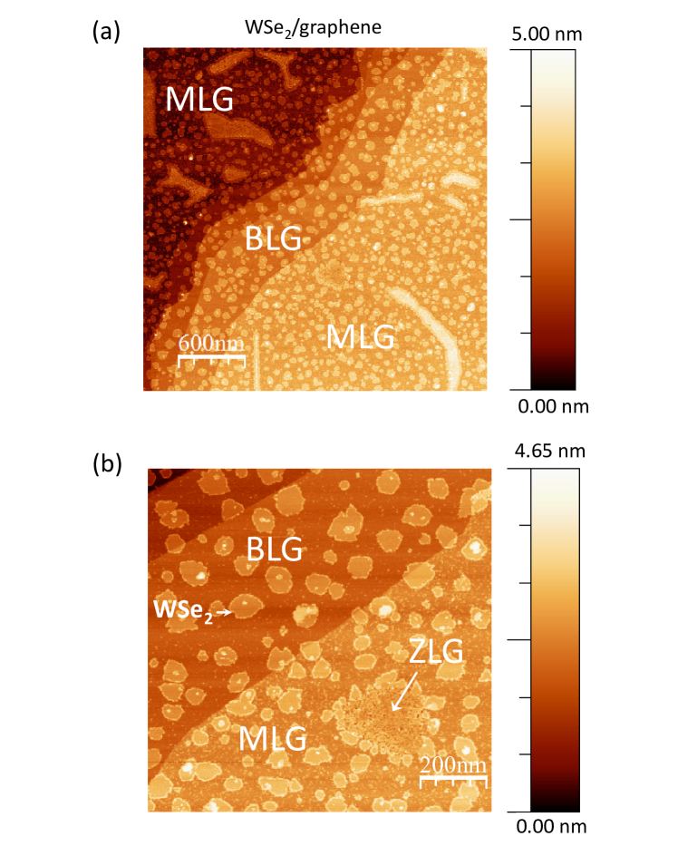
The morphology of monolayer WSe2 was measured by AFM. The unique feature of the -PLD grown films was a high spatial uniformity with relatively small island sizes. Larger scale AFM images show a high density of nucleation sites distributed uniformly over the surface [Fig. 5(a)]. The epitaxial graphene substrate had a minor inhomogeneity on the surface coming from the fabrication process, resulting in only small areas of bilayer graphene (BLG) close to the step edge, and other areas of exposed buffer layer (ZLG, which lacks a Dirac linear dispersion) within the flat MLG terrace region. Notably, WSe2 islands were indiscernible on ZLG by AFM [Fig. 5(b)]. On the other hand, islands on BLG tended to be larger (frequently approaching 100 nm) than on MLG [Fig. 5(b)]. The different WSe2 island sizes throughout the epitaxial graphene substrate are likely related to the distinct chemical nature and morphology of BLG, MLG and ZLG. During the TMD growth process, the migration of species could be severely limited on ZLG due to their covalent bonding to SiC and the resultant buckled surface sforzini , in contrast to the weak interaction on a complete vdW layers (MLG and BLG). For the latter, BLG regions may have even smoother surface than that of MLG regions due to the remoteness to the covalent bonds. Thus, our result clearly highlights the advantage of a chemically inert and smooth vdW surface in obtaining larger WSe2 domains during the epitaxial growth.
IV Summary and conclusions
A spin splitting of eV is found for the topmost WSe2 valence band at . The in-plane lattice constant of WSe2 was determined by grazing incidence X-ray diffraction, revealing a small compression ( %) of the epitaxial monolayer WSe2 film with respect to its bulk counterpart. Supplementing these data with first-principles calculations, we conclude that potential strain effects on are negligible in our WSe2 film. Furthermore, the overall band alignment between WSe2 and graphene was clarified. The electron transfer from graphene to WSe2 becomes apparent from an upshift of the Dirac point of graphene with respect to the Fermi level after the growth of the TMD monolayer. The varying WSe2 island sizes on substrate areas covered by graphene layers of different thicknesses suggest the importance of atomically smooth, weakly interacting van der Waals surfaces for monolayer TMD epitaxy. Our results provide high-quality data on both electronic and structural properties of monolayer WSe2 and shed light on potential substrate influences in bottom-up TMD growth.
Acknowledgements.
We are grateful to D. Huang and D. Weber for discussions and critical reading of the manuscript. We thank S. Prill-Drimmer, K. Pflaum, M. Dueller, and F. Adams for technical support. We acknowledge Diamond Light Source for time on Beamline I07 under Proposal SI18887 and Calipso program for the financial support. This work was supported by the Alexander von Humboldt-Foundation.References
- (1) K. F. Mak and J. Shan, Nat. Photon. 10, 216 (2016).
- (2) P. Rivera, H. Yu, K. L. Seyler, N. P. Wilson, W. Yao, and X. Xu, Nat. Nanotech. (2018); https://doi.org/10.1038/s41565-018-0193-0
- (3) G. Wang, A. Chernikov, M. M. Glazov, T. F. Heinz, X. Marie, T. Amand, and B. Urbaszek, Rev. Mod. Phys. 90, 021001 (2018).
- (4) K. F. Mak, D. Xiao, and J. Shan, Nat. Photon. 12, 451 (2018).
- (5) Q. H. Wang, K. K. Zadeh, A. Kis, J. N. Coleman, and M. S. Strano, Nat. Nanotechnol. 7, 699 (2012).
- (6) K. S. Novoselov, A. Mishchenko, A. Carvalho, and A. H. Castro Neto, Science 353, aac9439 (2016).
- (7) D. Xiao, G. B. Liu, W. Feng, X. Xu, and W. Yao, Phys. Rev. Lett. 108, 196802 (2012).
- (8) Z. Y. Zhu, Y. C. Cheng, and U. Schwingenschlögl, Phys. Rev. B 84, 153402 (2011).
- (9) H. Yuan, M. S. Bahramy, K. Morimoto, S. Wu, K. Nomura, B. J. Yang, H. Shimotani, R. Suzuki, M. Toh, C. Kloc, X. Xu, R. Arita, N. Nagaosa, and Y. Iwasa, Nat. Phys. 9, 563 (2013).
- (10) A. Srivastava, M. Sidler, A. V. Allain, D. S. Lembke, A. Kis, and A. Imamoğlu, Nat. Nanotechnol. 10, 491 (2015).
- (11) Y. M. He, G. Clark, J. R. Schaibley, Y. He, M. C. Chen, Y. J. Wei, X. Ding, Q. Zhang, W. Yao, X. Xu, C. Y. Lu, and J. W. Pan, Nat. Nanotechnol. 10, 497 (2015).
- (12) M. Koperski, K. Nogajewski, A. Arora, V. Cherkez, P. Mallet, J.-Y. Veuillen, J. Marcus, P. Kossacki, and M. Potemski, Nat. Nanotechnol. 10, 503 (2015).
- (13) C. Chakraborty, L. Kinnischtzke, K. M. Goodfellow, R. Beams, and A. N. Vamivakas, Nat. Nanotechnol. 10, 507 (2015).
- (14) Y. Luo, G. D. Shepard, J. V. Ardelean, D. A. Rhodes, B. Kim, K. Barmak, J. C. Hone, and S. Strauf, Nat. Nanotechnol. 13, 1137 (2018).
- (15) X. Lu, X. Chen, S. Dubey, Q. Yao, W. Li, X. Wang, Q. Xiong, and A. Srivastava, Nat. Nanotechnol. 14, 426 (2019).
- (16) Y. Zhang, T. R. Chang, B. Zhou, Y. T. Cui, H. Yan, Z. Liu, F. Schmitt, J. Lee, R. Moore, Y. Chen, H. Lin, H. T. Jeng, S. K. Mo, Z. Hussain, A. Bansil and Z. X. Shen, Nat. Nanotech. 9, 111 (2013).
- (17) M. H. Chiu, M. Y. Li, W. Zhang, W. T. Hsu, W. H. Chang, M. Terrones, H. Terrones, and L. J. Li, ACS Nano 8, 9649 (2014).
- (18) T. Eknapakul, P. D. C. King, M. Asakawa, P. Buaphet, R. H. He, S. K. Mo, H. Takagi, K. M. Shen, F. Baumberger, T. Sasagawa, S. Jungthawan, and W. Meevasana, Nano Lett. 14, 1312 (2014).
- (19) J. M. Riley, F. Mazzola, M. Dendzik, M. Michiardi, T. Takayama, L. Bawden, C. Granerød, M. Leandersson, T. Balasubramanian, M. Hoesch, T. K. Kim, H. Takagi, W. Meevasana, Ph. Hofmann, M. S. Bahramy, J. W. Wells and P. D. C. King, Nat. Phys. 10, 835 (2014).
- (20) D. Le, A. Barinov, E. Preciado, M. Isarraraz, I. Tanabe, T. Komesu, C. Troha, L. Bartels, T. S. Rahman, and P. A. Dowben, J. Phys.: Condesn. Mater 27, 182201 (2015).
- (21) Y. Zhang, M. M. Ugeda, C. Jin, S. F Shi, A. J. Bradley, A. Martín-Recio, H. Ryu, J. Kim, S. Tang, Y. Kim, B. Zhou, C. Hwang, Y. Chen, F. Wang, M. F. Crommie, Z. Hussain, Z. X. Shen, and S. K. Mo, Nano Lett. 16 2485 (2016).
- (22) K. E. Aretouli, P. Tsipas, D. Tsoutsou, J. Marquez-Velasco, E. Xenogiannopoulou, S. A. Giamini, E. Vassalou, N. Kelaidis, and A. Dimoulas, Appl. Phys. Lett. 106, 143105 (2015).
- (23) H. C. Diaz, J. Avila, C. Chen, R. Addou, M. C. Asensio, and M. Batzill, Nano Lett. 15 1135 (2015).
- (24) D. W. Latzke, W. Zhang, A. Suslu, T. R. Chang, H. Lin, H. T. Jeng, S. Tongay, J. Wu, A. Bansil, and A. Lanzara, Phys. Rev. B 91 235202 (2015).
- (25) J. M. Riley, W. Meevasana, L. Bawden, M. Asakawa, T. Takayama, T. Eknapakul, T. K. Kim, M. Hoesch, S. K. Mo, H. Takagi, T. Sasagawa, M. S. Bahramy, and P. D. C. King, Nat. Nanotech. 10, 1043 (2015).
- (26) K. Sugawara, T. Sato, Y. Tanaka, S. Souma, and T. Takahashi, Appl. Phys. Lett. 107, 071601 (2015).
- (27) K. E. Aretouli, D. Tsoutsou, P. Tsipas, J. Marquez-Velasco, S. A. Giamini, N. Kelaidis, V. Psycharis, and A. Dimoulas, ACS Appl. Mater. Interfaces 8, 23222 (2016).
- (28) S. K. Mo, C. Hwang, Y. Zhang, M. Fanciulli, S. Muff, J. H. Dil, Z. X. Shen, and Z. Hussain, J. Phys.: Condens. Matter 28, 454001 (2016).
- (29) Z. Ben Aziza, D. Pierucci, H. Henck, M. G. Silly, C. David, M. Yoon, F. Sirotti, K. Xiao, M. Eddrief, J. C. Girard, and A. Ouerghi, Phys. Rev. B 96 035407 (2017).
- (30) J. Binder, F. Withers, M. R. Molas, C. Faugeras, K. Nogajewski, K. Watanabe, T. Taniguchi, A. Kozikov, A. K. Geim, K. S. Novoselov, and M. Potemski, Nanoscale, 9, 16412 (2017).
- (31) H. Henck, Z. Ben Aziza, O. Zill, D. Pierucci, C. H. Naylor, M. G. Silly, N. Gogneau, F. Oehler, S. Collin, J. Brault, F. Sirotti, F. Bertran, P. L. Fèvre, S. Berciaud, A. T. C. Johnson, E. Lhuillier, J. E. Rault, and A. Ouerghi, Phys. Rev. B 96, 115312 (2017).
- (32) S. Agnoli, A. Ambrosetti, T. O. Mentes¸, A. Sala, A. Locatelli, P. L. Silvestrelli, M. Cattelan, S. Eichfeld, D. D. Deng, J. A. Robinson, J. Avila, C. Chen, and M. Carmen Asensio, ACS Appl. Nano Mater. 1, 1131 (2018).
- (33) N. R. Wilson, P. V. Nguyen, K. Seyler, P. Rivera, A. J. Marsden, Z. P. L. Laker, G. C. Constantinescu, V. Kandyba, A. Barinov, N. D. M. Hine, X. Xu, D. H. Cobden, Sci. Adv. 3, e1601832 (2017).
- (34) P. V. Nguyen, N. C. Teutsch, N. P. Wilson, J. Kahn, X. Xia, A. J. Graham, V. Kandyba, A. Giampietry, A. Barinov, G. Constantinescu, N. Yeung, N. D. M. Hine, X. Xu, D. H. Cobden, and N. R. Wilson, Nature 572, 220 (2019).
- (35) Y. Sun, R. Wang, and K. Liu, Appl. Phys. Rev. 4, 011301 (2017).
- (36) G. Froehlicher, E. Lorchat, and S. Berciaud, Phys. Rev. X 8, 011007 (2018).
- (37) K. V. Emtsev, A. Bostwick, K. Horn, J. Jobst, G. L. Kellogg, L. Ley, J. L. McChesney, T. Ohta, S. A. Reshanov, J. Röhrl, E. Rotenberg, A. K. Schmid, D. Waldmann, H. B. Weber, and Th. Seyller, Nat. Mater. 8, 203 (2009).
- (38) S. Forti and U. Starke, J. Phys. D 47, 094013 (2014).
- (39) C. Riedl, C. Coletti, and U. Starke, J. Phys. D: Appl. Phys. 43, 374009 (2010).
- (40) A. Mohammed, H. Nakamura, P. Wochner, S. Ibrahimkutty, A. Schulz, K. Müller, U. Starke, B. Stuhlhofer, G. Cristiani, G. Logvenov, and H. Takagi, Appl. Phys. Lett. 111, 073101 (2017).
- (41) C. Nicklin, T. Arnold, J. Rawle, and A. Warnea, J. Synchrotron Rad. 23, 1245 (2016).
- (42) P. Blaha, K. Schwarz, G. K. H. Madsen, D. Kvasnicka, and J. Luitz, WIEN2k, An Augmented Plane Wave + Local Orbitals Program for Calculating Crystal Properties, (Karlheinz Schwarz, Tech. Universität Wien, Vienna, 2001).
- (43) G. te Velde and E. J. Baerends , Phys. Rev. B 44, 7888 (1991).
- (44) BAND 2019.3, SCM, Theoretical Chemistry, Vrije Universiteit, Amsterdam, The Netherlands, http://www.scm.com
- (45) J. P. Perdew, K. Burke, and M. Ernzerhof, Phys. Rev. Lett. 77, 3865 (1996).
- (46) See Supplemental Material for the detail of ARPES EDC fitting to derive spin splitting, the lattice constant determination in GIXRD, as well as additional first-principles calculations with relaxed lattice.
- (47) W. J. Schutte, J. L. De Boer, and F. Jellinek, J. Solid. State. Chem. 70, 207 (1987).
- (48) J. Sforzini, L. Nemec, T. Denig, B. Stadtmüller, T.-L. Lee, C. Kumpf, S. Soubatch, U. Starke, P. Rinke, V. Blum, F. C. Bocquet, and F. S. Tautz, Phys. Rev. Lett. 114, 106804 (2015).
- (49) J. Ristein, S. Mammadov, and T. Seyller, Phys. Rev. Lett. 108, 246104 (2012).
- (50) S. Mammadov, J. Ristein, J. Krone, C. Raidel, M. Wanke, V. Wiesmann, F. Speck, and T. Seyller, 2D Mater. 4, 015043 (2017).