Realization of two-dimensional crystal of ions in a monolithic Paul trap
Abstract
We present a simple Paul trap that stably accommodates up to a couple of dozens ions in a stationary two-dimensional lattice. The trap is constructed on a single plate of gold-plated laser-machined alumina and can produce a pancake-like pseudo-potential that makes ions form a self-assembly two-dimensional crystal which locates on the plane composed of axial and one of the transverse axes with around 5 m spacing. We use Raman laser beams to coherently manipulate these ion-qubits where the net propagation direction is perpendicular to the plane of the crystal and micromotion. We perform the coherent operations and study the spectrum of vibrational modes through globally addressed Raman laser-beams on a dozen of ions in the two-dimensional crystal. We measure the amplitude of micro-motion by comparing the strengths of carrier and micro-motion sideband transitions with three ions, where the micro-motion amplitude is similar to that of a single ion. The spacings of ions are small enough for large coupling strengths, which is a favorable condition for two-dimensional quantum simulation.
Two-dimensional crystal of ions can be an attractive and natural platform to scale up the number of ion-qubits in a single trap and to explore many-body quantum models in two-dimension Britton et al. (2012); Bohnet et al. (2016); Chiaverini and Lybarger Jr (2008); Schmied et al. (2009); Clark et al. (2009, 2011); Sterling et al. (2014); Mielenz et al. (2016); Bermudez et al. (2011, 2012); Nath et al. (2015); Yoshimura et al. (2015); Richerme (2016); Wang et al. (2015); Jain et al. (2018); Goodwin et al. (2016). Recently, a fully-connected quantum computer has been realized with up to 5-20 ions forming one-dimensional (1D) crystal in linear Paul traps Debnath et al. (2016); Friis et al. (2018) and over 50 ion-qubits have been used for a quantum simulation with restricted controlZhang et al. (2017). Extra-dimension of the crystal can provide a quadratic scaling of the number of ion-qubits in the trap. Ion-qubits in the two-dimensional (2D) crystal intrinsically has 2D laser-induced interactions, which facilitates to study 2D many-body physics through quantum simulation such as geometric frustration, topological phase of matter, etc. Bermudez et al. (2011, 2012); Nath et al. (2015); Yoshimura et al. (2015); Richerme (2016).
There have been deliberate proposals and experimental exertions to confine ions in a 2D latticeBritton et al. (2012); Bohnet et al. (2016); Chiaverini and Lybarger Jr (2008); Schmied et al. (2009); Clark et al. (2009, 2011); Sterling et al. (2014); Mielenz et al. (2016); Jain et al. (2018); Szymanski et al. (2012); Tanaka et al. (2014); Yan et al. (2016). In the Penning trap that uses static magnetic field and dc voltages for the confinement, hundreds of ions form a rotating 2D crystal Mitchell et al. (1998). Effective Ising interactions among ion-qubits in the 2D crystal have been engineered Britton et al. (2012), and entanglement of spin-squeezing has been studied Bohnet et al. (2016). Due to a high magnetic field condition and the fast rotation of ions in Penning traps, however, no clock-state of an ion can represent an effective spin, and it is challenging to implement individual spin controls with laser beams.
Paul traps do not require high magnetic fields for confinement of ions and can be an alternative platform to implement 2D crystal. The main difficulty in Paul trap for producing 2D crystal of ions for quantum computation or quantum simulation lies in the existence of micromotion Berkeland et al. (1998) synchronous with the oscillating electric field that introduces phase modulations on laser beams for cooling and coherent operation. The micromotion can be nullified at a point or in a line, but not in a plane. To address the micromotion problem, arrays of micro traps have been proposed Chiaverini and Lybarger Jr (2008); Schmied et al. (2009) and small scale of arrays traps have been implemented Sterling et al. (2014); Mielenz et al. (2016). Due to relatively large distances between micro traps, however, the Coulomb-coupling strength between ion-qubits in different traps would be relatively weak and so as the effective spin-spin interactions induced by laser beams of coherent operations Welzel et al. (2011); Wilson et al. (2014); Hakelberg et al. (2019). Alternatively, it has been proposed to produce a trap, where the direction of micromotion is perpendicular to the net-propagation direction of laser beams for coherent control Yoshimura et al. (2015); Richerme (2016). Such a trap structure is relatively simple to manufacture and can easily hold tens to hundreds of ions.
Here, we report the implementation of a Paul trap that accommodates tens of ions in a 2D crystal. The trap is a three-dimensional monolithic trap Brownnutt et al. (2006); Shaikh et al. (2011); Wilpers et al. (2012) constructed on a single layer of gold-plated laser-machined alumina Hensinger et al. (2006); Madsen (2006). We carefully design the structure of the trap electrodes to precisely control the orientation of principle axis and ensure perpendicularity between the micromotion axis and the net-propagation direction of coherent operation Raman laser beams. The 2D crystal is located on the plane composed of axial and one of transverse axes, which is simply imaged to an electron-multiplying CCD (EMCCD) camera. We perform coherent operations on ion-qubits and study the spectrum of vibrational modes through globally addressed Raman laser beams. We measure the amplitude of micro-motion by comparing the strengths of carrier and micro-motion sideband transitions with three ions, where the modulation index similar to that of single ion. The strengths of effective spin-spin couplings can be similar to the values in current linear traps, which is a favorable condition for 2D quantum simulation.
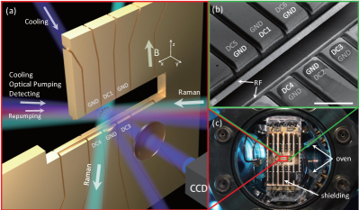
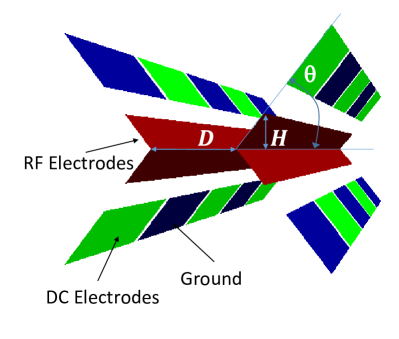
Our trap is fabricated in a single piece of alumina plate with gold-coating, with more details in Appendix B. Fig. 1 shows the structure of our trap. The trap is monolithic and functionally separated into three layers, where front and back layers contain dc electrodes, and the middle layer is used for RF electrode as conceptually shown in Fig. 1(a). The RF electrode has a slope with the angle of 45∘ relative to the normal direction of the alumina piece. In each DC layer, there are ten electrodes, five electrodes on both upside and downside with a 50 m spacing. At the center of the trap, there is a 260 m 4 mm slot, where ions are trapped. The Fig. 1(b) shows front side of the trap. The angle of the slope and the gap between DC and RF electrodes are optimized to maximize the trap frequency (see Appendix A for the design consideration). We use CPO (Charged Particle Optics) software to calculate the electric potential from the electrodes. We also compare the simulated potential with the real potential to calibrate the simulation coefficient for further trap simulation (see Appendix D). In the experiment, only six of twenty electrodes are connected to the stable DC sources, and the others to GND, as shown in Fig. 1(b).
The monolithic trap is located in a vacuum chamber shown in Fig 1(c). The trap and vacuum system is designed to ensure sufficient optical accesses. ions are loaded to the middle of the trap by photo-ionization and Doppler cooling Olmschenk et al. (2007). We create the 2D crystal of ions in a plane that consists of the axial axis (x-axis) and one of the radial axes (z-axis). We apply two Doppler-cooling laser beams to couple all the three directions of ion motions, as shown in Fig. 1(a). The magnetic-field insensitive states of ion in the ground-state manifold , and are mapped to qubit state and , respectively. The state of the qubit is detected by the laser beam resonant to the transition between of and of and initialized to by applying the optical pumping laser beam resonant with the transition between of and of . The qubit is coherently manipulated by a pair of 355 nm picosecond pulse laser beams with beatnote frequency about the qubit transition .
We rotate the principle axes of pseudo-potential in the y-z plane by adjusting voltages and on both of the center electrodes (DC1, DC2 in Fig. 1(b)) and all of the next to the center electrodes (DC3, DC4, DC5, and DC6 in Fig. 1(b)), respectively. The total pseudo-potential with voltages of , and is described by
| (1) |
where and are electric potentials at the position of generated by and electrodes with unit voltage. And is the pseudo-potential generated by the RF electrode with root-mean-square voltage of 1 V. In y-z plane, the symmetric RF pseudo-potential can be broken by DC potentials, which leads to a elliptical total potential . The two axes of the elliptical potential are the principle axes. In order to rotate the principle axes to y axis and z axis, we need to satisfy
| (2) |
where is related to the size of 2D crystal and small enough to be in harmonic regime for our consideration. Noticing is always true, we can calculate the solution of , to satisfy Eq. (2) based on numerical simulation. In our trap, . We should also notice that when ever we set to the right value and rotate the principle axes to y axis and z axis, will no longer affects the rotation of the principle axes.
We numerically calculate , and with CPO software. We set the RF signal to be MHz and V. When with V, vertical principle axis (green line in Fig. 2(a)) is clockwise rotated by 22.9∘ from the z-axis. When the ratio with V, the green axis is counter-clockwise rotated by 5.7∘ from the z-axis. As shown in Fig. 2(b), when the ratio , the green axis is in line with z-axis.
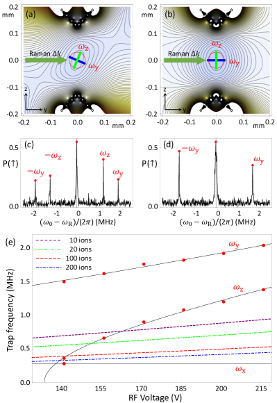
We experimentally confirm the rotation of the principle axes in y-z plane with single ion by observing the disappearance of the Raman coupling to z-axis vibrational mode. The spectrum of vibrational modes, as shown in Fig. 2(c)(d) is measured by the following procedure: 1) we perform Doppler cooling on ion-crystal, which results in thermal states with , Doppler cooling limit, and initialize the internal states to by applying the standard optical pumping technique. 2) We apply Raman beams with a net -vector perpendicular to the z-axis. Once the beatnote-frequency of Raman beams matching to , sideband transitions occurs Leibfried et al. (2003), which can be detected by the fluorescence of ions that is collected by imaging system and PMT (Photo-multiplier tube). In Fig. 2(c), the voltage ratio is close to the condition of in Fig. 2(a), where the principle axes are tilted away from y-z axes. The net -vector of Raman beams is along the y-axis, which can excite both directions of vibrational modes. Thus, two peaks in blue-sidebands as well as red-sidebands are clearly visible in Fig. 2(c), where detuning . However, when the principle axes are rotated to y-z axes as shown in Fig. 2(b), Raman beams cannot excite the vibrational mode along z-axis, which results in vanishing a peak in the Raman spectrum. Based on the spectrum of Fig. 2(d), we estimate that deviation of the principle axes from y-z axes is below .
In order to produce a 2D ion crystal in z-x plane, we need to satisfy Richerme (2016); Dubin (1993). First, keeping the principle axes to y-z axes, we can calculate the voltage solution for DC electrodes with a given axial trap frequency . With determined DC potential, the relation between and is given by Leibfried et al. (2003)
| (3) |
(see Appendix C) where is a positive constant determined by the trap geometry. In the case of , the z-axis potential, the shallower potential respective to that of the y-axis according to Eq. (3), becomes anti-harmonic, which indicates and . On the other hand, since are monotonously increase with , there is a critical value of that makes and . Therefore, we can tune from to , from near zero to by tuning . As shown in Fig. 2(e), with different values of , we can have from 0 to 2.72 for 10 ions to realize 2D ion crystal with different aspect ratios.
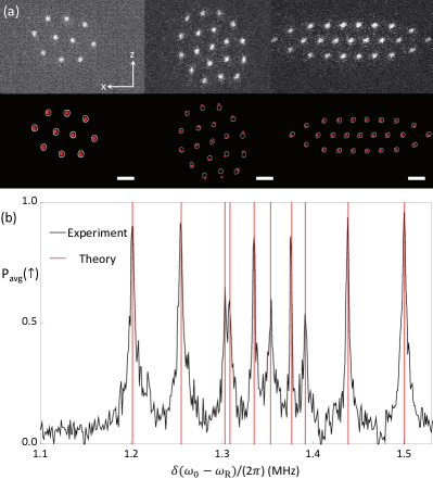
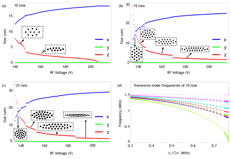
Once the requirements of principle axes and trap-frequencies for 2D crystal are satisfied as discussed above, we can confine ions in the xz-plane. Fortunately, the strongest trap frequency in our monolithic trap is in y-axis due to the geometry of the trap, which allows us to easily image the 2D crystal with the same imaging system to 1D chain. The fluorescence of ions in 2D crystal can be directly imaged through an objective lens to CCD camera as shown in Fig. 1(a). Figure 3(a) are the images of the 2D crystals and demonstrate the control capability for shapes of 2D crystals with various settings of trap frequencies. For the image of 10 ions, the trap frequencies are MHz. For the image of 19 ions and 25 ions the trap frequencies are MHz and MHz respectively. For 25 ions, these frequencies look violating the bound for the 2D crystal in Fig. 2(e). However, it is a complicated situation since one of the frequencies, , is still below the bound. We numerically study the situation carefully and discuss in the Appendix E. The geometries of the crystal are in agreement with the numerical simulation. We simulate the geometry configuration of the ion crystal by numerically minimizing the electrical potential of the ions in a three dimensional harmonic trap Richerme (2016).
We first verified the dimension of the crystal by imaging the crystal, but it is hard to distinguish whether there are any ions out of the ion crystal plane by an objective lens with finite depth of field. The dimension of the crystal is further verified by measuring the transverse mode structure. Similar to the single ion case, we drive the different transverse modes of a 10-ion crystal by varying the detuning between Raman beams. Fig 3(b) shows the resulting spectrum, where each peak represent a motional mode in the y-axis. The mode spectrum is consistent with the theoretical simulation based on trap frequencies and geometry of 2D ion crystalRicherme (2016). Similar to linear chain caseEnzer et al. (2000), when the phase transition from a 2D crystal to a 3D crystal happens the minimal frequency of the mode along the y-axis will tend to be negative. Our measured mode frequencies are far away from zero, which confirm the dimension of the crystal is two.
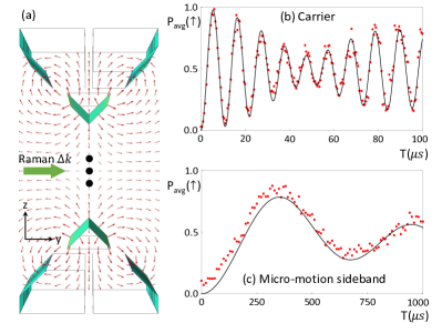
Ideally, if the crystal is located in the z-x plane, the direction of micro-motion is along the z-axis and perpendicular to the y-axis, which is the net propagation direction of Raman beams. In practice, there are two possible imperfection sources that make the crystal deviate from the ideal micro-motion condition: 1) Stray electric field, which induces displacement; 2) Fabrication imperfection of the electrodes, which induces the tilt around the z-axis. To minimize the micro-motion from theses sources, we first compensate the straight field with a single-ion, then mitigate the tilt errors by slightly rotating the crystal. With the single ion, the micro-motion compensation is done by overlapping the position of the ion to the null point of the RF electric field Berkeland et al. (1998). We first compensate the extra-field in z direction by changing the voltage of or DC1,DC5,DC6 simultaneously with the ratio 1,5.11,5.11, which is able to keep the principle axes direction and avoid generating the displacement along y axis. We can also change the voltage of electrodes DC1,DC3,DC4 or DC2,DC5,DC6 with ratio 1,5.11,5.11 to compensate the extra-field in y direction. For the z-axis compensation, we minimize the change of ion position depending on RF power and for the y-axis compensation, we minimize the micro-motion sideband transition of Raman beams. For the error induced by the fabrication imperfection, we slightly change the voltage of electrodes DC3,DC4,DC5,DC6 with ratio 1,1,1,1 to rotate the crystal around x axis and with ratio 1,-1,1,-1 to rotate the crystal around z axis. With the control, we also minimize the Rabi-frequency of the micro-motion sideband transition with three ions.
The strength of the micro-motion is quantified by measuring the ratio between two Rabi frequencies of the carrier and the micro-motion transitionBerkeland et al. (1998). We measure the micro-motion strength in a three-ion 2D crystal. We first sequentially apply Doopler cooling and EIT cooling qiao and in preperation to cool the 2D crystal down to near the motional ground state. Then we drive the Rabi flopping and measure the Rabi frequency of the carrier and the micro-motion sideband transition. For each flopping, we collect the overall counts of three ions with PMT and fit the result with three Rabi frequency. The fitting gives us three carrier -time 5.96, 5.40, 5.19s and three micro-motion sideband -time 474, 440, 317s. The modulation index, which is given by , has a maximun possible value of and a minimal possible value of , which are similar to single ion situation.
We also experimentally study the heating of the vibrational modes in our trap with a single ion. We first prepare the ground-state of radial vibrational modes by Raman-sideband cooling, wait for a certain duration and measure average phonon-number for the mode of interest. We estimate by Fourier transforming the blue-sideband transitions Leibfried et al. (2003). We find that the heating rate of y-axis mode with the principle axes of 2D crystal (Fig. 2(b)) is around 360 quanta per second, which is about 2.5 times larger than that with the condition of Fig. 2(a). It is understandable, since the noise of environmental electric field along y-axis would be more severe than those of the other axes.
Our trap can be considered as an ideal platform for implementing various proposals of quantum simulations with 2D crystal Bermudez et al. (2011, 2012); Nath et al. (2015); Yoshimura et al. (2015); Richerme (2016). It can be used to observe a structural quantum phase transition from 2D to 3D with relaxed requirementsMorigi (2019). Incorporating the capability of individual control and detection, universal quantum computation also can be achieved with more number of qubits than in a linear chain. The capability of laser addressing in a two dimensional space has been demonstrated with different techniquesCrain et al. (2014); McGloin et al. (2003). The detection of individual ions already has been well established using camera with high detection efficiency Myerson et al. (2008).
Furthermore, the 2D crystal is a natural platform for the fault-tolerant quantum computation schemes with 2D geometry, including the surface codeBombin and Martin-Delgado (2006), the Bacon-Shor codeAliferis and Cross (2007) and the (2+1) dimensional fault-tolerant measurement-based quantum computingRaussendorf et al. (2007); Bombin (2018); Newman et al. (2019). The full connectivity of trapped-ion system provides the capability of implementing any fault-tolerant scheme without extra overhead at the circuit levelLi et al. (2019). However, to implement a 2D topological code on an 1D ion chain, one has to map some local interactions to long distance gates or shuttle the ions, which requires longer gate timeBermudez et al. (2017); Trout et al. (2018); Blumel et al. (2019). With a 2D ion crystal, the locality of 2D topological codes can be preserved, without the loss of full connectivity.
Acknowledgments
We thank Jincai Wu and Haifeng Zhu at Interstellar Quantum Technology (Nanjing) Ltd for many useful discussions on fabrication technique. This work was supported by the National Key Research and Development Program of China under Grants No. 2016YFA0301900 and No. 2016YFA0301901 and the National Natural Science Foundation of China Grants No. 11374178, No. 11574002, and No. 11974200.
Y.W. and M.Q contributed equally to this work.
I APPENDIX
II APPENDIX A: STRUCTURE OF THE TRAP
We use CPO software to simulate the trap performance with various geometric parameters. There are three important parameters for the trap design: the distance between two RF electrodes , the height of RF electrodes , and the angle of the slope as shown in Fig 5. We optimize these three parameters mainly to achieve large secular frequencies in the radial direction given fabrication limitation. The secular frequency is approximately inverse-proportional to Leibfried et al. (2003), which is inspected in our numerical simulation. We balance the requirement of large trap frequency and low UV-light scattering, which leads to the choice of m. For the slope angle , our simulation shows the best performance at . Due to the fabrication difficulty of the angle, we choose . Our simulation shows the best value of is around m. Considering the laser cutting precision, we decide m.
III APPENDIX B: FABRICATION PROCESS
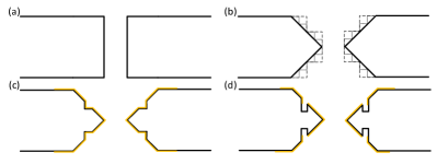
The substrate is a single piece of alumina with the thickness of 380 m and the surface flatness of less than 30 nm. The electronic structure is fabricated by the laser-machining and coated with 3 m gold by electroplating technology. The detailed procedure to fabricate the electrodes structure is as follows: 1) Carve a slot of 260 m at the center of the piece, as shown in Fig. 6(a); 2) Make a slope of 45∘ on each side by cutting small steps to fit the slope as shown in Fig. 6(b); 3) Make a tiny groove on each slope. The width of the groove is around 50 m; 4) Do gold coating on both sides of the chip as shown in Fig. 6(c); 5) Cut deeper in the groove position to remove gold. The center layer is electrically separated with top and bottom layer; 6) Laser cut the slots on top and bottom layer to electrically separate all DC electrodes. Among all the steps, the second is the subtlest one. The geometry of the four slopes is crucial for the ion control with DC voltages. In step 2), for each slope, we apply 40 times of laser cutting with different duration and 5 m shift on cutting position. The cutting duration for each pulse is calculated base on the calibrated relationship between the cutting depth and the cutting time. The laser cutting precision is 1 m, which is limited by the worktable instability. Using a laser with the power of 2W, the wavelength of 355 nm and the beam waist of around 15 m, we can have the cutting speed to be 100 mm/s.
IV APPENDIX C: TRAP FREQUENCY CALCULATION
According to Ref. Leibfried et al. (2003), we can write the time dependent potential of the trap as follows:
where is the voltage applied on the DCE electrode, , , are geometric factors determined by the geometry of the DCE electrode, is the root mean square of the voltage applied on RF electrode, , and are geometric factors determined by the geometry of the RF electrode. We note that x,y and z axes in the Eq. (IV) should be three principle axes of the trap potential. All the geometric factors will change based on the different rotation of the principle axes. The condition that the potential has to fulfill the Laplace equation leads to the restrictions as follows:
| (5) | |||
| (6) |
With our symmetric RF electrodes in the axial direction, it’s clear that , which leads to . Solving the Mathieu equation for three directions, we can have the results as:
| (7) | |||
| (8) | |||
| (9) |
Due to , we can have
| (10) |
This equation explains the Eq. (3) in the main text. As we mentioned before, all the geometric factors are determined by the rotation of the principle axes.
V APPENDIX D: TRAP SIMULATION CALIBRATION
Due to the fabrication imperfection, the real trap potential may deviate from the ideal model in simulation. We develop a method to quantitatively calibrate difference between the reality and the simulation, which is useful for the further simulation and the prediction of the trap behavior. Take as an example, we can describe difference between the reality and the simulation as follows:
| (11) |
where is the real potential generated by electrode DCC along the x-axis, is the simulated potential, and is the imperfection coefficient for DCC in x-axis. We study the relationship between the real axial trap frequency and the simulated axial trap frequency to calibrate .
We start from calculating the axial mode frequency, which is . By using the expression of in Eq. (1), we can have
| (12) |
With the Eq. (12) and fixed value of , we can treat as a linear function with , which has the slope as and the intercept as . We can write two version of Eq. (12)
| (13) | ||||
| (14) |
where
| (15) | |||
| (16) |
So we know
| (17) |
Combining Eq. (13), Eq. (14) and Eq. (17), with the same value of , we can have
| (18) |
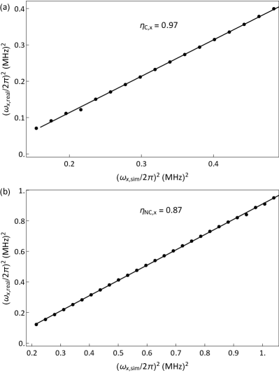
where is an intercept determined by and geometries of other electrodes. We measured axial trap frequency by adding a modulation signal on one of the DC electrodes and checking the ion image. When the modulation frequency is close to the axial mode frequency, the motion of the ion is resonantly excited and melting in the axial direction. By changing and plotting the points {} in Fig. 7(a), we can fit the coefficient of . By doing same measurement but only changing , we can obtain . is close to 1, which means the geometry of the center electrodes is near perfect in the axial direction. On the other side, indicate that DCNC electrodes are further away from the ion in the reality than in the simulation. Whenever we want to simulate the axial potential, we need to include and in consideration.
To calibrate the imperfection coefficients of two radial principle axes, y-axis and z-axis, we execute the same procedure as the axial calibration with more careful consideration about the principle-axes rotation. During the process of changing or , only if we keep the rotation angle of the principle axes in a small regime, we can have the similar equations as Eq. (18) for y-axis and z-axis:
| (19) | ||||
| (20) | ||||
| (21) | ||||
| (22) |
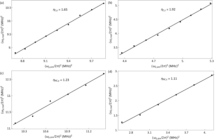
All the data is shown in Fig. 8. From the data and the linear fitting, we can obtain , , and . All these imperfection coefficients are larger than 1, which indicates that all, relative to the ideal model, the DC electrodes are closer to the ion in the radial direction in the reality. When we simulate the radial potential and check the principle axes rotation in yz-plane, we use the average value and to be the coefficients multiplied to and .
VI APPENDIX E: GEOMETRY OF ION CRYSTAL AND SIMULATION OF MODE FREQUENCIES
We calculate the dashed lines in Fig. 2(e) using the formula Richerme (2016), where varies with the RF voltage. When and are both bigger than , the ions form a 3D crystal. When and are both smaller than the bound, the ions from a 2D crystal. However, when two frequencies are not larger or smaller than the bound at the same time, there is no simple expression of the critical point for the phase transition from a 2D crystal to a 3D crystal. For example, if one of the modes is below the bounds while the another above, the ions can still form a 2D crystal. We can imagine such a situation from a homogeneous crystal where . In this case the ions form a 3D crystal not 2D, but if we release the confinement along the x-axis by lowering , at a certain , the ions can form a 2D crystal. We verify this situation for 10, 19, and 25 ions by numerically simulating the equilibrium positions of the ions and study the structures of the crystals if they are in 2D as shown in Fig. 9.
As mentioned in the main text, in the region near the phase transition from 2D to 3D, the minimal frequency of the transverse modes will tends to zero. We also numerically study this behavior on a 10-ion 2D crystal and the show the result in Fig. 9 (d).
References
- Britton et al. (2012) J. W. Britton, B. C. Sawyer, A. C. Keith, C.-C. J. Wang, J. K. Freericks, H. Uys, M. J. Biercuk, and J. J. Bollinger, Nature 484, 489 (2012).
- Bohnet et al. (2016) J. G. Bohnet, B. C. Sawyer, J. W. Britton, M. L. Wall, A. M. Rey, M. Foss-Feig, and J. J. Bollinger, Science 352, 1297 (2016).
- Chiaverini and Lybarger Jr (2008) J. Chiaverini and W. Lybarger Jr, Phys. Rev. A 77, 022324 (2008).
- Schmied et al. (2009) R. Schmied, J. H. Wesenberg, and D. Leibfried, Phys. Rev. Lett. 102, 233002 (2009).
- Clark et al. (2009) R. J. Clark, T. Lin, K. R. Brown, and I. L. Chuang, J. Appl. Phys. 105, 013114 (2009).
- Clark et al. (2011) R. J. Clark, Z. Lin, K. S. Diab, and I. L. Chuang, J. of Appl. Phys. 109, 076103 (2011).
- Sterling et al. (2014) R. C. Sterling, H. Rattanasonti, S. Weidt, K. Lake, P. Srinivasan, S. Webster, M. Kraft, and W. K. Hensinger, Nature Commun. 5, 3637 (2014).
- Mielenz et al. (2016) M. Mielenz, H. Kalis, M. Wittemer, F. Hakelberg, U. Warring, R. Schmied, M. Blain, P. Maunz, D. L. Moehring, D. Leibfried, et al., Nature Commun. 7, 11839 (2016).
- Bermudez et al. (2011) A. Bermudez, J. Almeida, F. Schmidt-Kaler, A. Retzker, and M. B. Plenio, Phys. Rev. Lett. 107, 207209 (2011).
- Bermudez et al. (2012) A. Bermudez, J. Almeida, K. Ott, H. Kaufmann, S. Ulm, U. Poschinger, F. Schmidt-Kaler, A. Retzker, and M. Plenio, New J. Phys. 14, 093042 (2012).
- Nath et al. (2015) R. Nath, M. Dalmonte, A. W. Glaetzle, P. Zoller, F. Schmidt-Kaler, and R. Gerritsma, New J. Phys. 17, 065018 (2015).
- Yoshimura et al. (2015) B. Yoshimura, M. Stork, D. Dadic, W. C. Campbell, and J. K. Freericks, EPJ Quan. Tech. 2, 2 (2015).
- Richerme (2016) P. Richerme, Phys. Rev. A 94, 032320 (2016).
- Wang et al. (2015) S.-T. Wang, C. Shen, and L.-M. Duan, Sci. Rep. 5, 8555 (2015).
- Jain et al. (2018) S. Jain, J. Alonso, M. Grau, and J. P. Home, arXiv preprint arXiv:1812.06755 (2018).
- Goodwin et al. (2016) J. F. Goodwin, G. Stutter, R. C. Thompson, and D. M. Segal, Physical review letters 116, 143002 (2016).
- Debnath et al. (2016) S. Debnath, N. M. Linke, C. Figgatt, K. A. Landsman, K. Wright, and C. Monroe, Nature 536, 63 (2016).
- Friis et al. (2018) N. Friis, O. Marty, C. Maier, C. Hempel, M. Holzäpfel, P. Jurcevic, M. B. Plenio, M. Huber, C. Roos, R. Blatt, et al., Phys. Rev. X 8, 021012 (2018).
- Zhang et al. (2017) J. Zhang, G. Pagano, P. W. Hess, A. Kyprianidis, P. Becker, H. Kaplan, A. V. Gorshkov, Z.-X. Gong, and C. Monroe, Nature 551, 601 (2017).
- Szymanski et al. (2012) B. Szymanski, R. Dubessy, B. Dubost, S. Guibal, J.-P. Likforman, and L. Guidoni, Appl. Phys. Lett. 100, 171110 (2012).
- Tanaka et al. (2014) U. Tanaka, K. Suzuki, Y. Ibaraki, and S. Urabe, J. Phys. B 47, 035301 (2014).
- Yan et al. (2016) L. Yan, W. Wan, L. Chen, F. Zhou, S. Gong, X. Tong, and M. Feng, Sci. Rep. 6, 21547 (2016).
- Mitchell et al. (1998) T. Mitchell, J. Bollinger, D. Dubin, X.-P. Huang, W. Itano, and R. Baughman, Science 282, 1290 (1998).
- Berkeland et al. (1998) D. Berkeland, J. Miller, J. C. Bergquist, W. M. Itano, and D. J. Wineland, J. Appl. Phys. 83, 5025 (1998).
- Welzel et al. (2011) J. Welzel, A. Bautista-Salvador, C. Abarbanel, V. Wineman-Fisher, C. Wunderlich, R. Folman, and F. Schmidt-Kaler, Eur. Phys. J. D 65, 285 (2011).
- Wilson et al. (2014) A. C. Wilson, Y. Colombe, K. R. Brown, E. Knill, D. Leibfried, and D. J. Wineland, Nature 512, 57 (2014).
- Hakelberg et al. (2019) F. Hakelberg, P. Kiefer, M. Wittemer, U. Warring, and T. Schaetz, Phys. Rev. Lett. 123, 100504 (2019).
- Brownnutt et al. (2006) M. Brownnutt, G. Wilpers, P. Gill, R. Thompson, and A. Sinclair, New J. Phys. 8, 232 (2006).
- Shaikh et al. (2011) F. Shaikh, A. Ozakin, J. M. Amini, H. Hayden, C.-S. Pai, C. Volin, D. R. Denison, D. Faircloth, A. W. Harter, and R. E. Slusher, arXiv:1105.4909 (2011).
- Wilpers et al. (2012) G. Wilpers, P. See, P. Gill, and A. G. Sinclair, Nature Nanotech. 7, 572 (2012).
- Hensinger et al. (2006) W. Hensinger, S. Olmschenk, D. Stick, D. Hucul, M. Yeo, M. Acton, L. Deslauriers, C. Monroe, and J. Rabchuk, Appl. Phys. Lett. 88, 034101 (2006).
- Madsen (2006) M. J. Madsen, Advanced ion trap development and ultrafast laser-ion interactions, Ph.D. thesis, University of Michigan (2006).
- Olmschenk et al. (2007) S. Olmschenk, K. C. Younge, D. L. Moehring, D. N. Matsukevich, P. Maunz, and C. Monroe, Phys. Rev. A 76, 052314 (2007).
- Leibfried et al. (2003) D. Leibfried, R. Blatt, C. Monroe, and D. Wineland, Rev. Mod. Phys. 75, 281 (2003).
- Dubin (1993) D. H. Dubin, Phys. Rev. Lett. 71, 2753 (1993).
- Enzer et al. (2000) D. Enzer, M. Schauer, J. Gomez, M. Gulley, M. Holzscheiter, P. G. Kwiat, S. Lamoreaux, C. Peterson, V. Sandberg, D. Tupa, et al., Physical review letters 85, 2466 (2000).
- (37) M. qiao and K. K. in preperation, .
- Morigi (2019) G. Morigi, “Kinks and defects in ion crystals,” https://www.youtube.com/watch?v=JvOkdS1zGPY&list=PLCoSh1h28ieLt-_gy-JXqogKBxmN_p7el&index=19&t=0s (2019).
- Crain et al. (2014) S. Crain, E. Mount, S. Baek, and J. Kim, Applied Physics Letters 105, 181115 (2014).
- McGloin et al. (2003) D. McGloin, G. C. Spalding, H. Melville, W. Sibbett, and K. Dholakia, Optics Express 11, 158 (2003).
- Myerson et al. (2008) A. Myerson, D. Szwer, S. Webster, D. Allcock, M. Curtis, G. Imreh, J. Sherman, D. Stacey, A. Steane, and D. Lucas, Physical Review Letters 100, 200502 (2008).
- Bombin and Martin-Delgado (2006) H. Bombin and M. A. Martin-Delgado, Physical review letters 97, 180501 (2006).
- Aliferis and Cross (2007) P. Aliferis and A. W. Cross, Physical review letters 98, 220502 (2007).
- Raussendorf et al. (2007) R. Raussendorf, J. Harrington, and K. Goyal, New Journal of Physics 9, 199 (2007).
- Bombin (2018) H. Bombin, arXiv preprint arXiv:1810.09571 (2018).
- Newman et al. (2019) M. Newman, L. A. de Castro, and K. R. Brown, arXiv preprint arXiv:1909.11817 (2019).
- Li et al. (2019) M. Li, D. Miller, M. Newman, Y. Wu, and K. R. Brown, Physical Review X 9, 021041 (2019).
- Bermudez et al. (2017) A. Bermudez, X. Xu, R. Nigmatullin, J. O’Gorman, V. Negnevitsky, P. Schindler, T. Monz, U. Poschinger, C. Hempel, J. Home, et al., Physical Review X 7, 041061 (2017).
- Trout et al. (2018) C. J. Trout, M. Li, M. Gutiérrez, Y. Wu, S.-T. Wang, L. Duan, and K. R. Brown, New Journal of Physics 20, 043038 (2018).
- Blumel et al. (2019) R. Blumel, N. Grzesiak, and Y. Nam, arXiv preprint arXiv:1905.09292 (2019).