Magnetic-Field-Induced Transition in a Quantum Dot Coupled to a Superconductor
Abstract
The magnetic moment of a quantum dot can be screened by its coupling to a superconducting reservoir, depending on the hierarchy of the superconducting gap and the relevant Kondo scale. This screening-unscreening transition can be driven by electrostatic gating, tunnel coupling, and, as we demonstrate here, magnetic field. We perform high-resolution spectroscopy of subgap excitations near the screening-unscreening transition of asymmetric superconductor - quantum dot - superconductor (S–QD–S) junctions formed by the electromigration technique. Our measurements reveal a re-entrant phase boundary determined by the competition between Zeeman energy and gap reduction with magnetic field. We further track the evolution of the phase transition with increasing temperature, which is also evidenced by thermal replicas of subgap states.
The junction between a superconductor and a quantum dot displays discrete subgap energy levels called Andreev bound states (ABS) or, more specifically, Yu-Shiba-Rusinov (YSR) states when the highest occupied level hosts a single spin Balatsky et al. (2006); Heinrich et al. (2018). When the antiferromagnetic exchange interaction between this spin and the leads prevails over the superconducting gap , the localized spin is effectively Kondo screened, and a quasiparticle is bound at the interface. In contrast, if the exchange coupling is weaker, the superconducting condensate is marginally perturbed and the spin remains unscreened. The change between these two distinct ground states occurs via a sharp level crossing, which constitutes a simple realization of a quantum phase transition. In recent years, detailed investigations of this screening-unscreening transition have been performed, using as a control knob the variation of the level depth Deacon et al. (2010); Pillet et al. (2010); Lee et al. (2014); Jellinggaard et al. (2016); Assouline et al. (2017) or the tunnel coupling, which effectively modifies the exchange coupling strength Franke et al. (2011); Island et al. (2017); Farinacci et al. (2018); Malavolti et al. (2018). The variation of an external magnetic field may provide an additional parameter with twofold consequences: increasing the magnetic field suppresses superconducting correlations (hence favoring a screened state), while the Zeeman effect enhances polarization towards one of the magnetic YSR states Lee et al. (2014); Jellinggaard et al. (2016); Li et al. (2017); Cornils et al. (2017). Thus, the two effects associated to a magnetic field lead to a shifting of level crossing in opposite directions.
Experimentally, it is challenging to explore the effect of the magnetic field on the screening-unscreening transition, precisely for the reason that superconductivity is usually quenched before the quantum phase transition can be accessed. Hence, the quantum dot systems needs to be tuned close to the critical point using another control parameter, here the back gate voltage allowed in our transistor geometry. Furthermore, the detection of tiny level shifts between subgap states requires exquisite energy resolution in the V range, which can be achieved only with superconducting leads.
In this Letter, we report on the observation of the magnetic field-controlled screened-unscreened ground state transition of a quantum dot strongly coupled to one superconducting lead. An asymmetrically coupled superconductor–quantum dot–superconductor (S-QD-S) device combines the gate tunability of single electron transistors with the unprecedented spectroscopic resolution of the subgap states. Monitoring the dispersion of the subgap states allows tracking the transition between the screened and unscreened spin ground states of the quantum dot as a function of the bare level of the dot, temperature, and, most importantly, magnetic field. We use the Anderson impurity as the main framework for the modelization of our data. A general phase diagram is drawn, which demonstrates a striking re-entrant behavior of the phase boundary, due to the previously mentioned competition between Zeeman splitting and superconducting gap closing. In addition, thermal replicas of YSR states are found to emerge at finite temperature, providing an alternative yet consistent picture of the subgap spectrum.
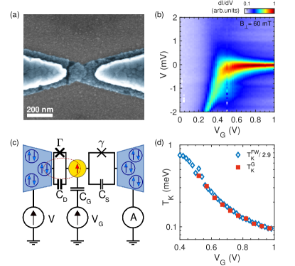
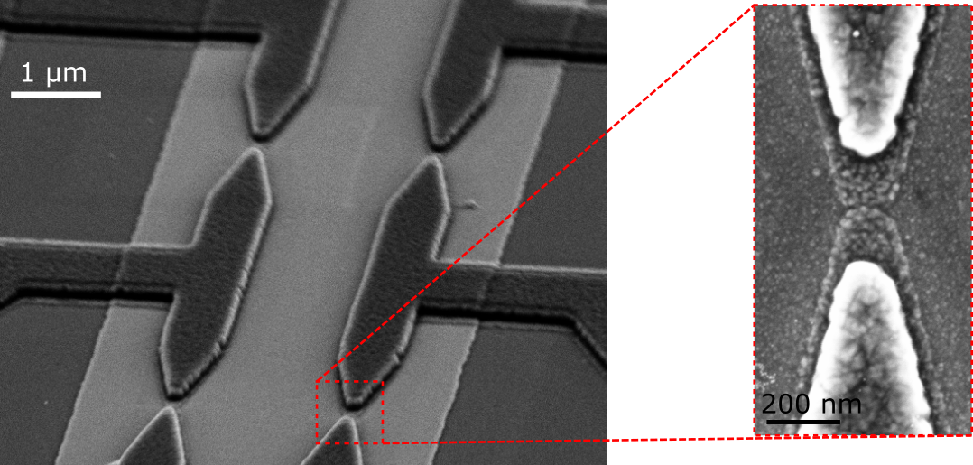
The device fabrication process relies on controlled electromigration of an on-chip all-metallic aluminum device presenting a constriction Park et al. (1999). This technique produces nanometer sized gaps and was successfully applied for connecting single molecules Park and McEuen (2000); Park et al. (2002); Liang et al. (2002); Vincent et al. (2012). Electrostatic gate control is provided through a local metallic back gate isolated by a 18 nm thick Zr02 dielectric layer. Using aluminum as the constriction material, gated S–QD–S devices can thereby be formed Winkelmann et al. (2009); van Zanten et al. (2015, 2016). Our quantum dots are colloidal gold nanoparticles of 5 nm diameter. Electromigration is performed at 4.2 K in cryogenic vacuum in a dilution cryostat. A scanning electron micrograph of an Al constriction after electromigration (without nanoparticles, for better visibility) is shown in Fig. 1a. Samples showing stable gate-dependent conductance features are further investigated at temperatures down to mK. The differential conductance is measured using the lock-in technique, as a function of bias and gate voltage . We show here data mostly from one sample, labelled A. Data from a second and similar sample (B) can be found in the Supplemental Material file.
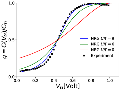
The normal state differential conductance map (obtained at a magnetic field of 60 mT) is shown in Fig. 1b, around the only experimentally accessible degeneracy point at V. To the left, the linear conductance is suppressed, owing to a Coulomb-blockaded state with an even electron occupation number . As the gate voltage is increased, a zero-bias resonance indicates the onset of Kondo correlations associated to the spin-1/2 degeneracy of the oddly occupied electron state. The electrical model of the quantum dot junction is displayed in Fig. 1c. The tunnel couplings to both leads are strongly asymmetric (), as evidenced by a non-unitary linear conductance limit, , with (see Supplemental Material file). This implies notably that the Kondo resonance builds between the QD and the drain electrode at experimentally accessible temperatures, the source contact acting as a tunnel probe, as it is usually the case for the tip in an STM experiment. The following values of hybridization meV and Coulomb repulsion meV in the quantum dot are found from fits of the gate-dependent zero-bias conductance to Numerical Renormalization Group (NRG) calculations, see Supplemental Material. The ratio shows that the quantum dot is in the strongly correlated regime, with some deviations from Kondo scaling.
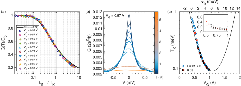
The full-width at half-maximum (FWHM) of the conduction resonance at the Fermi level, as shown in Fig. 1b, is often taken as an approximate measure of the Kondo temperature , that we note (here and later we set , identifying temperature and energy scales). Another direct and precise determination of is achieved considering the measured temperature dependence of the linear conductance . The latter can be fitted by NRG calculations, or for a lower computational cost, by an empirical expression Goldhaber-Gordon et al. (1998a); Dutta et al. (2019), leading to the gate-dependent Kondo temperature denoted shown in Fig. 1d (see also Supplemental Material). We find that these estimates agree closely within a scaling factor, such that . Therefore, it is seen that the quantum dot junction behaves like a single spin-1/2 Kondo impurity, with a gate-tunable that can be brought to the same order of magnitude as the superconducting order parameter of the leads, leading to a standard gate-control of the screening transition Bauer et al. (2007); Maurand et al. (2012).
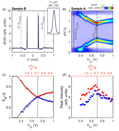
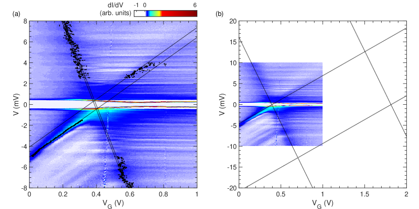
We now turn to the study of the S–QD–S transistor at zero magnetic field. In presence of superconductivity in both leads, a transport gap of total width eV opens in the transport map, see Fig. 2b. The Kondo peak is suppressed and two sharp symmetric resonances appear at a certain biasing voltage so that . We take care to differentiate the gap eV of the strongly coupled lead, which governs the physical effects at play, from the gap eV of the weakly coupled electrode, which offsets essentially the conductance onset thresholds by . Thermal excitations at 940 mK provide unambiguous evidence of the probe’s gap size (see Fig. 4a)
The presence of the YSR states is reflected by extremely sharp subgap resonances (Fig. 2a) at , that is, when the probe’s chemical potential allows for driving the dot to its excited state by either adding or removing an electron. The transport mechanisms leading to a d.c. current here are essentially based on Andreev processes Ruby et al. (2015). From the experimental gate dependence of the bound state spectrum , the singlet-doublet ground state transition, occurring for , is readily seen to occur near V. Note that owing to the very sharply defined gap edge of aluminum van Zanten et al. (2015), but also low experimental temperatures and careful shielding of the experiment, we can achieve a spectroscopic resolution down to a FWHM of less than 10 eV (Fig. 2a), way below previously reported line widths. The latter have indeed been discussed as a lifetime limiting factor in possible subgap state-based qubits Pillet et al. (2010); Zazunov et al. (2003).
Combining our knowledge of the superconducting and normal state properties, we can now plot the bound state dispersion as a function of gate voltage , which we express as a function of the dimensionless ratio (Fig. 2c). We find the transition to the unscreened ground state for the critical value , consistent with Ref. Buizert et al. (2007) or with the value in Ref. Bauer et al. (2013). Theoretical calculations Bauer et al. (2007) predict a critical value , using the scaling formula . While we can rescale our data to (for instance at the value at the center of the diamond), which gives a reasonable value , we emphasize that our device is not strictly in the scaling regime where these predictions apply quantitatively Meden (2019). In addition, a calculation using renormalized ABS theory Meng et al. (2009) allows us to obtain a full gate-dispersion of the bound state in good agreement with the experimental observation, see Fig. 2c and Supplemental Material file for details. Furthermore, the intensities of the conductance peaks, which reflect the weigths carried by bound states, also follow the expected behaviour Bauer et al. (2007) across the ground state transition, as shown in Fig. 2d.
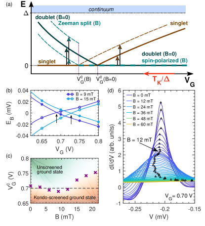
Having understood in detail the zero-field properties of the QD–S hybrid, we now move to the main result of this work, in which we evidence the competition of two magnetic effects on the ground state transition of the quantum dot. A magnetic field is expected to Zeeman split the two spin projections of the doublet state by , with the gyromagnetic factor and the Bohr magneton. The effect of the Zeeman splitting on the doublet state has been observed in superconductor - quantum dot junctions formed in semiconducting nanowires, owing to the large in these materials Lee et al. (2014); Jellinggaard et al. (2016); Li et al. (2017). In these works, the sub-gap resonances are Zeeman split at the singlet ground state phase because two excited states are accessible. In contrast, when the singlet is the excited state, no splitting was seen, because the only possible transition (at low temperature ) is from the lower energy spin-polarized state to the singlet.
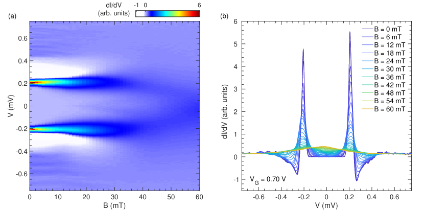
Beyond the mere spectroscopic effect of the Zeeman splitting of the doublet excited state at a given dot level depth, we now consider the magnetic field effect on the ground state transition itself. Indeed, as one of the spin projections of the unscreened spin state has a lower energy, the screened ground state phase space gradually shrinks, which is translated here into a critical value of moving to lower values. This is sketched in Fig. 3a and precisely observed in Fig. 3c, where we plot the critical gate value associated to the ground state transition as a function of magnetic field. The latter is determined as previously from the kink (crossing) in the YSR dispersion, for each applied magnetic field as shown in Fig. 3b. For small fields mT, there is a clear downward trend of , indicating a Zeeman-driven reduction of the parameter space associated to the singlet ground state. As the magnetic field is further increased, the reduction of the superconducting gap starts coming into play, with a quadratic magnetic field dependence of the gap to lowest order Anthore et al. (2003). Intuitively, the gradual weakening of superconductivity favors Kondo screening of the spin in the dot, and thereby favors the singlet ground state, enhancing again the critical (Fig. 3c). This re-entrance of the phase-boundary is confirmed when sweeping the magnetic field at a fixed gate voltage V (Fig. 3d). The transition of the ground state parity induced near a field of 12 mT is accompanied by an abrupt change in the YSR spectra, which move to higher energies and acquire a broader lineshape (see Supplemental Material file for details).
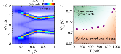
For completeness, we finally focus on the effect of higher temperatures for the tunnelling spectroscopies as well as the ground state transition. First, at higher temperatures, the non-zero probability of finding the dot in its excited state allows for new conductance resonances in tunneling spectroscopies emerging at , which are commonly referred to as thermal replicas of the YSR resonances. This is readily seen as a pair of new peaks at low voltages in Fig. 4a. The corresponding values of the bound state energy can now also be deduced from the related supplementary threshold conditions, in excellent agreement with the bound state energies deduced from the main resonances, leading to the data shown in Fig. 4b. The singlet-doublet transition can thus be equally observed from the thermal replicas. Second, the thermal weakening of the superconducting gap provides another method for tuning the singlet-doublet ground state transition. At mK, we indeed find that the transition has moved to a larger gate value, about V (or equivalently at a lower than for the base temperature), in agreement with expectations. Obviously, no re-entrance is observed in the temperature dependence of the transition.
In conclusion, we have demonstrated a magnetic field tuning of the screening-unscreening transition of a quantum dot coupled to superconductors in a transistor geometry. A novel phase diagram was established, demonstrating that the magnetic field leads to a re-entrant transition due to the competition between Zeeman stabilisation of the lowest spin-polarised orbital and weakening of the superconducting gap. A complementary finite temperature phase diagram was drawn, that reflects the sole thermal weakening on the superconducting gap, while signatures of the ground state transition were also observed in thermally excited replicas. These results demonstrate that quantum dots constitute a rich model system for the controlled exploration of strong correlations effects in nanostructures. Further developments will address the influence of the screening-unscreening transition on operational properties of single electron turnstiles van Zanten et al. (2016).
This work was funded by the joint ANR-DFG grant JOSPEC and the Labex LANEF programme. Samples were fabricated at the Nanofab facility at Institut Néel-CNRS and PTA-CEA. We thank D. Basko, J. Pekola, N. Hatter and B. Heinrich for useful discussions.
References
- Balatsky et al. (2006) A. V. Balatsky, I. Vekhter, and J.-X. Zhu, “Impurity-induced states in conventional and unconventional superconductors,” Rev. Mod. Phys. 78, 373–433 (2006).
- Heinrich et al. (2018) B. W. Heinrich, J. I. Pascual, and K. J. Franke, “Single magnetic adsorbates on s-wave superconductors,” Prog. Surf. Sci. 93, 1–19 (2018).
- Deacon et al. (2010) R. S. Deacon, Y. Tanaka, A. Oiwa, R. Sakano, K. Yoshida, K. Shibata, K. Hirakawa, and S. Tarucha, “Tunneling spectroscopy of Andreev energy levels in a quantum dot coupled to a superconductor,” Phys. Rev. Lett. 104, 076805 (2010).
- Pillet et al. (2010) J.-D. Pillet, C. H. L. Quay, P. Morfin, C. Bena, A. Levy Yeyati, and P. Joyez, “Andreev bound states in supercurrent-carrying carbon nanotubes revealed,” Nat. Phys. 6, 965–969 (2010).
- Lee et al. (2014) E. J. H. Lee, X. Jiang, M. Houzet, R. Aguado, C. M. Lieber, and S. De Franceschi, “Spin-resolved Andreev levels and parity crossings in hybrid superconductor–semiconductor nanostructures,” Nat. Nanotechnol. 9, 79 (2014).
- Jellinggaard et al. (2016) A. Jellinggaard, K. Grove-Rasmussen, M. H. Madsen, and J. Nygård, “Tuning Yu-Shiba-Rusinov states in a quantum dot,” Phys. Rev. B 94, 064520 (2016).
- Assouline et al. (2017) A. Assouline, C. Feuillet-Palma, A. Zimmers, H. Aubin, M. Aprili, and J.-C. Harmand, “Shiba bound states across the mobility edge in doped InAs nanowires,” Phys. Rev. Lett. 119, 097701 (2017).
- Franke et al. (2011) K. J. Franke, G. Schulze, and J. I. Pascual, “Competition of superconducting phenomena and Kondo screening at the nanoscale,” Science 332, 940–944 (2011).
- Island et al. (2017) J. O. Island, R. Gaudenzi, J. de Bruijckere, E. Burzurí, C. Franco, M. Mas-Torrent, C. Rovira, J. Veciana, T. M. Klapwijk, R. Aguado, and H. S. J. van der Zant, “Proximity-induced Shiba states in a molecular junction,” Phys. Rev. Lett. 118, 117001 (2017).
- Farinacci et al. (2018) L. Farinacci, G. Ahmadi, G. Reecht, M. Ruby, N. Bogdanoff, O. Peters, B. W. Heinrich, F. von Oppen, and K. J. Franke, “Tuning the coupling of an individual magnetic impurity to a superconductor: quantum phase transition and transport,” Phys. Rev. Lett. 121, 196803 (2018).
- Malavolti et al. (2018) L. Malavolti, M. Briganti, M. Hänze, G. Serrano, I. Cimatti, G. McMurtrie, E. Otero, P. Ohresser, F. Totti, M. Mannini, R. Sessoli, and S. Loth, “Tunable spin-superconductor coupling of spin 1/2 vanadyl phtalocyanine molecules,” Nano Letters 18, 7955–7961 (2018).
- Li et al. (2017) S. Li, N. Kang, P. Caroff, and H.Q. Xu, “0– phase transition in hybrid superconductor–InSb nanowire quantum dot devices,” Phys. Rev. B 95, 014515 (2017).
- Cornils et al. (2017) L. Cornils, A. Kamlapure, L. Zhou, S. Pradhan, A. A. Khajetoorians, J. Fransson, J. Wiebe, and R. Wiesendanger, “Spin-resolved spectroscopy of the Yu-Shiba-Rusinov states of individual atoms,” Phys. Rev. Lett. 119, 197002 (2017).
- Park et al. (1999) H. Park, A. K. L. Lim, A. P. Alivisatos, J. Park, and P. L. McEuen, “Fabrication of metallic electrodes with nanometer separation by electromigration,” Appl. Phys. Lett. 75, 301–303 (1999).
- Park and McEuen (2000) H. Park and P. L. McEuen, “Nano-mechanical oscillations in a single-C60 transistor,” Nature 407, 57–60 (2000).
- Park et al. (2002) J. Park, A. N. Pasupathy, J. I. Goldsmith, C. Chang, Y. Yaish, J. R. Petta, M. Rinkoski, J. P. Sethna, H. D. Abruña, and P. L. McEuen, “Coulomb blockade and the Kondo effect in single-atom transistors,” Nature 417, 722–725 (2002).
- Liang et al. (2002) W. Liang, M. P. Shores, M. Bockrath, J. R. Long, and H. Park, “Kondo resonance in a single-molecule transistor,” Nature 417, 725–729 (2002).
- Vincent et al. (2012) R. Vincent, S. Klyatskaya, M. Ruben, W. Wernsdorfer, and F. Balestro, “Electronic read-out of a single nuclear spin using a molecular spin transistor,” Nature 488, 357 (2012).
- Winkelmann et al. (2009) C. B. Winkelmann, N. Roch, W. Wernsdorfer, V. Bouchiat, and F. Balestro, “Superconductivity in a single-C60 transistor,” Nat. Phys. 5, 876–879 (2009).
- van Zanten et al. (2015) D. M. T. van Zanten, F. Balestro, H. Courtois, and C. B. Winkelmann, “Probing hybridization of a single energy level coupled to superconducting leads,” Phys. Rev. B 92, 184501 (2015).
- van Zanten et al. (2016) D. M. T. van Zanten, D. M. Basko, I. M. Khaymovich, J. P. Pekola, H. Courtois, and C. B. Winkelmann, “Single quantum level electron turnstile,” Phys. Rev. Lett. 116, 166801 (2016).
- Goldhaber-Gordon et al. (1998a) D. Goldhaber-Gordon, H. Shtrikman, D. Mahalu, D. Abusch-Magder, U. Meirav, and M. A. Kastner, “Kondo effect in a single-electron transistor,” Nature 391, 156–159 (1998a).
- Dutta et al. (2019) B. Dutta, D. Majidi, A. García-Corral, P. A Erdman, S. Florens, T. A. Costi, H. Courtois, and C. B. Winkelmann, “Direct probe of the Seebeck coefficient in a Kondo-correlated single-quantum-dot transistor,” Nano Lett. 19, 506–511 (2019).
- Bauer et al. (2007) J. Bauer, A. Oguri, and A. C. Hewson, “Spectral properties of locally correlated electrons in a Bardeen–Cooper–Schrieffer superconductor,” J. Phys.: Condens. Matter 19, 486211 (2007).
- Maurand et al. (2012) R. Maurand, T. Meng, E. Bonet, S. Florens, L. Marty, and W. Wernsdorfer, “First-Order 0- Quantum Phase Transition in the Kondo Regime of a Superconducting Carbon-Nanotube Quantum Dot,” Phys. Rev. X 2, 011009 (2012).
- Ruby et al. (2015) M. Ruby, F. Pientka, Y. Peng, F. von Oppen, B. W. Heinrich, and K. J. Franke, “Tunneling Processes into Localized Subgap States in Superconductors,” Phys. Rev. Lett. 115, 087001 (2015).
- Zazunov et al. (2003) A. Zazunov, V. S. Shumeiko, E. N. Bratus, J. Lantz, and G. Wendin, “Andreev level qubit,” Phys. Rev. Lett. 90, 087003 (2003).
- Buizert et al. (2007) C. Buizert, A. Oiwa, K. Shibata, K. Hirakawa, and S. Tarucha, “Kondo universal scaling for a quantum dot coupled to superconducting leads,” Phys. Rev. Lett. 99, 136806 (2007).
- Bauer et al. (2013) J. Bauer, J. I. Pascual, and K. J. Franke, “Microscopic resolution of the interplay of Kondo screening and superconducting pairing: Mn-phthalocyanine molecules adsorbed on superconducting Pb (111),” Phys. Rev. B 87, 075125 (2013).
- Meden (2019) V. Meden, “The Anderson-Josephson quantum dot - A theory perspective,” J. Phys.: Cond. Mat. 31, 163001 (2019).
- Meng et al. (2009) T. Meng, S. Florens, and P. Simon, “Self-consistent description of Andreev bound states in Josephson quantum dot devices,” Phys. Rev. B 79, 224521 (2009).
- Anthore et al. (2003) A. Anthore, H. Pothier, and D. Estève, “Density of states in a superconductor carrying a supercurrent,” Phys. Rev. Lett. 90, 127001 (2003).
- Thijssen and Van der Zant (2008) J. M. Thijssen and Herre S. J. Van der Zant, “Charge transport and single-electron effects in nanoscale systems,” physica status solidi (b) 245, 1455–1470 (2008).
- Choi et al. (2004) M.-S. Choi, M. Lee, K. Kang, and W. Belzig, “Kondo effect and Josephson current through a quantum dot between two superconductors,” Phys. Rev. B 70, 020502 (2004).
- Buitelaar et al. (2002) M. R. Buitelaar, T. Nussbaumer, and C. Schönenberger, “Quantum dot in the Kondo regime coupled to superconductors,” Phys. Rev. Lett. 89, 256801 (2002).
- Cronenwett et al. (1998) S. M. Cronenwett, T. H. Oosterkamp, and L. P. Kouwenhoven, “A tunable Kondo effect in quantum dots,” Science 281, 540–544 (1998).
- Lee et al. (2017) E. J. H. Lee, X. Jiang, R. Aguado, C. M. Lieber, S. De Franceschi, et al., “Scaling of subgap excitations in a superconductor-semiconductor nanowire quantum dot,” Phys. Rev. B 95, 180502 (2017).
- Goldhaber-Gordon et al. (1998b) D. Goldhaber-Gordon, J. Göres, M. A. Kastner, H. Shtrikman, D. Mahalu, and U. Meirav, “From the Kondo regime to the mixed-valence regime in a single-electron transistor,” Phys. Rev. Lett. 81, 5225 (1998b).
- Affleck et al. (2000) I. Affleck, J.-S. Caux, and A. M. Zagoskin, “Andreev scattering and Josephson current in a one-dimensional electron liquid,” Phys. Rev. B 62, 1433–1445 (2000).
- Tanaka et al. (2007) Y. Tanaka, A. Oguri, and A. C. Hewson, “Kondo effect in asymmetric Josephson couplings through a quantum dot,” New J. Phys. 9, 115 (2007).
- Vecino et al. (2003) E. Vecino, A. Martin-Rodero, and A. Levy Yeyati, “Josephson current through a correlated quantum level: Andreev states and junction behavior,” Phys. Rev. B 68, 035105 (2003).
- Wentzell et al. (2016) N. Wentzell, S. Florens, T. Meng, V. Meden, and S. Andergassen, “Magnetoelectric spectroscopy of Andreev bound states in Josephson quantum dots,” Phys. Rev. B 94, 085151 (2016).
- Court et al. (2007) N. A. Court, A. J. Ferguson, and R. G. Clark, “Energy gap measurement of nanostructured aluminium thin films for single Cooper-pair devices,” Superconductor Science and Technology 21, 015013 (2007).
- Levy-Bertrand et al. (2019) F. Levy-Bertrand, T. Klein, T. Grenet, O. Dupré, A. Benoît, A. Bideaud, O. Bourrion, M. Calvo, A. Catalano, A. Gomez, et al., “Electrodynamics of granular aluminum from superconductor to insulator: Observation of collective superconducting modes,” Phys. Rev. B 99, 094506 (2019).
- Shanenko et al. (2008) A. A. Shanenko, M. D. Croitoru, and F. M. Peeters, “Superconducting nanofilms: Andreev-type states induced by quantum confinement,” Phys. Rev. B 78, 054505 (2008).
Supplemental Information File: Magnetic-Field-Induced Transition in a Quantum Dot Coupled to a Superconductor
This supporting information discusses the sample fabrication process of electromigrated superconducting quantum dots, the electrical characterization of the Kondo-correlated quantum dot in both the normal and superconducting state, and presents a second sample showing similar physics to the one discussed in the main text. Theoretical modeling is also developed in detail, including Numerical Renormalization Group (NRG) calculations used to extract microscopic parameters of the device, as well as the determination of Andreev Bound state dispersions from renormalized perturbation theory.
I Sample fabrication
The substrates employed for the fabrication of gated electromigration junctions are 2-inch intrinsic silicon wafers with a native oxide layer and a resistivity larger than 8000 cm. Three steps of lithography, followed by the corresponding metal deposition and lift-off, are carried out. First, a local back-gate is patterned by optical laser lithography using a bi-layer resist of LOR3A/S1805. After development, a deposition of 3 nm of \ceTi followed by 30 nm of \ceAu is done on the sample with an electron beam evaporator and put into lift-off solvent. Then the sample surface is cleaned with a reactive ion etching oxygen plasma of 20 watts power for 5 minutes, and a \ceZrO2 oxide layer of approximately 18 nm is conformally grown by atomic layer deposition (ALD) technique. In the second lithography step, the bonding pads and access lines are patterned with a hard-mask UV aligner on a LOR3A/UV3 bi-layer resist. The sample is then metallized with 3 nm of Ti plus 50 nm of Au and put into lift-off solvent. Electron-beam lithography is employed to pattern the bow-tie shaped constriction on top of the oxide-covered gate electrode in the last lithography step. A bi-layer resist of PMMA/MMA AR-P 617.06 and PMMA 3% is used to create a stable undercut by proximity effect of the beam. Suspended resist bridges at the narrowest part of the constrictions result from this undercut. By performing a double angle evaporation of 14 nm of \ceAl fixing the sample at angles of w.r.t. the axis perpendicular to the gate electrode, nano-constrictions are grown below each undercut bridge (as shown in Fig. S5).
The process finishes with a perpendicular evaporation of 80 nm of \ceAl to decrease the access lines resistance. Few hundreds of individual chips are fabricated simultaneously from a 2-inch wafer, each containing 30 \ceAl electromigration constrictions divided in two arrays. A colloidal toluene suspension of 5 nm diameter \ceAu nano-particles (functionalized with dodecanethiol ligands) is dropcasted several times on the surface of an individual chip the same day that it is glued and bonded to a sample-holder and inserted in a dilution cryostat. Electromigration is performed inside the fridge at a cryogenic temperature of about K. Junctions displaying a tunneling current with gate-dependent features are further investigated at dilution temperatures of mK (increasing to 100 mK for magnetic field experiments). Around 100 aluminum constrictions have been successfully electromigrated in the work of the present article. Several of these breaking tunnel junctions presented a gate dependent current, but only 4 displayed an identifiable diamond-like structure in the stability diagram and sub-gap current that indicated the presence of bound states. Out of 4, only 2 (samples A and B) had a gate dependence stable enough to acquire systematic successive measurements.
II Extracting experimental parameters from NRG
Strongly correlated quantum dots are generically described by a single-level impurity model involving two electrodes (left/right, or drain/source), according to the Anderson Hamiltonian:
| (S1) |
assuming that confinement is strong enough to disregard fully occupied or empty orbitals. Here creates an electron on the dot with spin , and an electron in the lead with spin and momentum . The parameters of the model in Eq. (S1) are the single-particle energy level of the quantum dot (relative to the equilibrium Fermi level of the leads, taken as energy reference), the local Coulomb repulsion on the dot, the kinetic energy of the lead electrons, and the tunneling amplitude from the dot to electrode . Taking into account a generic asymmetry between the coupling to each electrode, we define the respective hybridizations as and , with the electronic density of states at the Fermi level (assumed identical in both electrodes, without loss of generality). Typically, in a tunneling geometry relevant for the present experiment, one has . In addition, a voltage bias , originating from an imbalance of the chemical potentials in each lead, allows to drive a current through the nanostructure, and forms the basis of conductance measurements in electronic quantum dot devices.
We define a bonding orbital and its corresponding orthonormal antibonding orbital, so that the antibonding orbital decouples from the tunneling process via the dot level. The total hybridization of the -level is thus , since in a tunneling geometry. This allows to use a single channel Anderson model in equilibrium, which simplifies the numerical simulations. A Kondo resonance in the dot density of states develops provided in the local moment regime where charge dynamics is frozen by Coulomb blockade, but spin fluctuations associated to the dot orbital assist transport through the nanostructure. One defines also the mixed valence regime between the empty and single occupied quantum dot as .
The most crucial microscopic parameter of Hamiltonian in Eq. (S1) to be extracted from the experiment is the ratio , which sets the strength of electronic correlations. Standard Coulomb diamond spectroscopy cannot be used in the regime where Kondo correlations are fully developed due to many-body modification of the excitations’ linewidth. A more reliable method is to use the gate dependence of the zero-bias conductance, which is readily obtained from linear response theory:
| (S2) | |||||
| (S3) |
with the zero-temperature finite frequency density of states of the impurity level, assuming that the base temperature is well below the Kondo scale. We model in Eq. (S3) a linear relation between the level position and the applied gate voltage , with the gate lever arm, and the offset voltage corresponding to the center of the Coulomb diamond in the experiment, so that implies (particle-hole symmetric point). The maximum value for allowed by Friedel sum rule is , a value that is attained at the center of the odd charge Coulomb diamond (namely ) at zero temperature. We define a rescaled dimensionless conductance that crosses over from 0 (in the empty dot regime ) to 1 (at the center of the odd charge diamond ). The lineshape of is interesting to estimate correlations because it forms a flat plateau of width proportional to , and displays a crossover on a scale of the order of . In addition, is weakly sensitive to the electronic bandwidth, provided that it is larger than hybridization (not shown). Since is mostly controlled by the single scale , this ratio can be extracted precisely from a scaling analysis. A comparison of the experimental measurement to the NRG data is shown in Fig. S6. We have chosen here three values of , and fixed the ratio , where is the half-bandwidth of the electrodes. The horizontal axis corresponds to the experimental voltage , and a small charge offset artifact was removed from the experimental data in order to produce a smooth curve. This results in a small offset of the center of the Coulomb diamond expected near V. Regarding the rescaling of the NRG data, we apply a similar centering to the Coulomb diamond center, . Then we convert the energy level to voltage from the multiplicative form . For each NRG curve, we choose so that the normalized NRG conductance crosses the experimental points at the mid point . This allow to test the scaling form of for various values of the parameters. We find that our experimental data are best fitted for the value . One notices a slight decrease of , below the unitary limit, in the experimental data for the largest values. Such a thermal effect is expected from the finite temperature (100 mK) at which the measurements were done.
III Characterization of sample A
The nanometric crack appearing in electromigrated constrictions after the breaking procedure has normally an irregular shape and the distance between the two resulting leads is variable along the constriction section, often below 1 nm at certain spots. Usually, a tunneling current directly from one lead to the other is measurable, bypassing any possible quantum dot and originating a conductance background. We start the characterization of the sample by measuring the linear shunt resistance of the junction, , away from the degeneracy point in the even occupation side. We found M at V in sample A.
III.1 Coulomb blockade analysis
The well-known diamond like structure of blocked current regions appearing in the stability diagram of gated-quantum dot junctions become blurred in the presence of higher order transport processes (like the spin-flip Kondo resonance), enhanced due to a high relative tunnel coupling energy scale (). An appropriate extraction of the diamond features is crucial to determine quantitatively the relevant parameters of the quantum dot junction, such as its degeneracy point position () in the gate voltage dimension, its capacitive coupling to the source, drain and gate electrodes ( respectively) and its charging energy . The sharp density of states of the superconducting \ceAl leads promotes the diamond edges differential conductance, allowing us to perform linear fits of the corresponding conductance maxima, as shown in Fig. S7a. Adapting Coulomb blockade standard analysis methods Thijssen and Van der Zant (2008) to our particular case of superconducting leads, the degeneracy point is found to be at V from the middle point between the crossing of the linear fits at , in excellent correspondence with the mid point at which the measured zero-bias conductance of the Kondo resonance decreases by half, providing a criterium to select the numerical values of for the comparison of the NRG simulations in Fig. S6 with the experimental data. The experimental gate lever arm and the source–drain capacitance asymmetry have been determined from the extracted positive ( meV/V) and negative ( meV/V) diamond edges slopes using the following relations:
| (S4) |
| (S5) |
The high source–drain capacitance asymmetry derived for sample A is reflected in a few orders of magnitude difference in the tunnel couplings (calculated later in this section), leading to a probing configuration of a strongly coupled system, commonly reached in scanning electron microscopy experiments. The small value, typical from single molecule/nano-particle transistors, does not allow to observe the next degeneracy point () of the quantum dot junction. However, as explained in the following, we performed a parabolic fit of the Kondo temperature gate dependence that indicates the position of the Coulomb diamond center to be close to V. An extrapolation of the next degeneracy point can be done so that V (see Fig. S7b), leading to a charging energy of meV, in good agreement with the value found for the experimental gate coupling of around 0.9 %.
III.2 Alternative Kondo temperature extraction methods
Different criteria can be found in the literature for the experimental extraction of the Kondo energy scale () in quantum dot junctions. The lack of a general definition valid for all regimes of relative energy scales complicates the fitting and comparison of results for samples involving different ratios between , and . For quantum dot junctions identified to be in the Kondo regime (), a possible zero-temperature definition is , valid only at the center of the odd diamond (). Although the dependence remains the same Choi et al. (2004), in a generic electrostatic configuration within the Coulomb diamond (namely ) the proportionality factor is not well-defined:
| (S6) |
Experimentally, is often extracted from the full width at half maximum (FWHM) of the Kondo zero-bias peak, with a variable multiplicative factor Buitelaar et al. (2002); Cronenwett et al. (1998); Franke et al. (2011); Maurand et al. (2012); Bauer et al. (2013); Lee et al. (2017) generally equal to 1/2. However, thermal broadening and reduction of the resonance, conductance backgrounds and slight shifts in the relative energy scales can induce a non-negligible mismatch between different experiments in Kondo-regime systems. Alternatively, an empirical expression deducted from the NRG model was proposed by Goldhaber-Gordon et. al. Goldhaber-Gordon et al. (1998b), as a rigorous method for extracting , based on the universal dependence of the relative resonance maxima conductance with temperature:
| (S7) |
where represents the zero bias conductance at zero temperature (as explained in the first section II), represents the conductance background of the junction (typically , and is a fitting parameter found to be around for magnetic Kondo impurities with spin 1/2. In symmetrically coupled quantum dot junctions in the Kondo regime measured at zero temperature, is expected to reach the quantum of conductance around the center of the odd diamond (). In contrast, in an asymmetric case where one lead has a reduced coupling down to the so-called sequential regime (), the absence of Kondo correlations with this weakly coupled lead () modulates the peak intensity of the Kondo resonance (only present at the strongly coupled lead), leading to a strong reduction w.r.t. to the unitary value:
| (S8) |
In our sample configuration, the presence of a gate electrode allows us to modify the quantum dot chemical potential ( up to an arbitrary offset at ), leading to a gate-tunable parameter. We have measured and performed a least squares fit of at different temperatures of sample A with Goldhaber-Gordon’s Eq. (S7), for each accessible value of (Fig. S8a).
The resulting values of were found by setting (since the differential conductance away from the degeneracy point ( V) decreases below of ), and imposing an extrapolated conductance at zero temperature of (Fig. S8b). Additionally, the value of can be plugged in Eq. (S8), leading to a tunnel coupling asymmetry of . Combining the conclusions obtained from NRG simulations for the relative energy scales value of with the extraction of meV from the Coulomb blockade analysis, we derive the tunnel couplings to be meV and eV.
The Kondo resonance FWHM, measured as a function of bias voltage and at a base temperature of mK ( eV), displays an identical gate-driven renormalization, albeit for a scaling factor of 1/2.9 w.r.t. to the previous temperature-based extraction (Fig. S8c). The natural logarithm of the extracted displays a clear parabolic dependence that can be fitted with the previously given definition in Eq. (S6), using the extracted value for to determine . This quadratic fit provides an alternative way of extracting the energy scales and , obtaining 12.5 meV and 2.5 meV respectively. Although the resulting is extremely close to the value inferred from the Coulomb Blockade analysis (12.7 meV), this sample is not deep enough in the Kondo regime, as derived from the NRG simulations (), so that the quadratic fit can be only taken into account qualitatively. However, the overall tendency of variation with is well described by the fitting parabola, leading us to designate the center of the blocked diamond () employed in the Coulomb blockade analysis from its minimum at about 1.1 V. As approaches , the system enters into the mixed valence regime (), where Eq. (S6) is not valid anymore and the tendency of the gate dependence changes. Although the least squares fitting method still provides a normalizing value for voltages of 0.52 V and 0.57 V, and the temperature dependence of the experimental data follows the universal behavior in rather good agreement, we observe in the inset of Fig. S8c (where is represented linear scale) that the standard deviation suffers a sudden increase, reaching values around 0.2 meV. Therefore, the corresponding values (shown in Fig. S8c as unframed squares) cannot be highly trusted, and have not been taken into account for fitting the parabola.
III.3 Magnetic field behavior in the superconducting state
When turning the strongly coupled lead into the superconducting state, Yu-Shiba-Rusinov (YSR) subgap excitations emerge from the competition between the superconducting electron pairing () and the Kondo correlations induced by the oddly-occupied quantum dot Franke et al. (2011), probed at different by the weakly coupled lead, which is also in superconducting state. As discussed in the main article, the crossing of the YSR resonances at zero energy indicates a phase transition happening at (at a critical gate voltage value of V), where both of the ground states at each side of the critical point (the Kondo singlet at the 0-phase and the unscreened doublet at the -phase) undergo an inversion, becoming the excited state at the contrary side.
By applying an external magnetic field () perpendicular to the sample surface, it is possible to quench superconductivity, turning the leads into the normal state, suppressing the superconducting energy scale . In Fig. S9 we can observe how the spectroscopic gap (with a total range of mV at mT) decreases as is increased, and has completely disappeared at mT. Accordingly, the YSR peaks decrease their intensity and finally merge into the Kondo resonance at zero bias, much broader and less intense. Tuning the gate to 0.70 V, close to the critical point (at = 0.71 V), and measuring the spectrum at different , a gentle oscillation in the energy of the negative bias YSR peak can be observed, as shown in the zoomed-in graph of Fig. 3d in the main article. In order to further investigate this phenomenon, we measured whole differential conductance maps (analogous to that one shown in Fig. S7a) at different fixed values of . The critical gate position displays an apparent oscillation, reaching a minimum value at 9 mT. This downwards tendency, enlarging the -phase effective area is a consequence of the Zeeman splitting of the excited state at the 0-phase, that displaces the phase boundary position. For increasing above 9 mT, the quenching of superconductivity in the lead gradually reduces the effective , favoring the dominance of the 0-phase, i.e. the formation of the Kondo singlet.
IV Andreev bound states dispersion from renormalized perturbation theory
In presence of superconductivity, we supplement the Anderson impurity model (S1) with a pairing contribution in the electrodes: , with the superconducting gap in the left and right lead respectively. In order to gain some insight, we discuss first briefly the large gap solution of the superconducting Anderson model Affleck et al. (2000); Tanaka et al. (2007); Bauer et al. (2013); Vecino et al. (2003), and make as previously the assumption of asymmetric tunneling, . The bare Green’s function of the dot indeed becomes purely local for (we use here Nambu notation):
| (S9) |
which derives from an effective local Hamiltonian
| (S10) |
to which one can add the interaction term controlled by the Coulomb repulsion . Diagonalizing the full local Hamiltonian using a Bogoliubov basis transformation provides four discrete Andreev eigenstates with the eigenvalues:
| (S11) |
where correspond to spin polarized singly occupied states, while are proximity induced superpositions of the empty and doubly occupied states (BCS-like states). We have noted , the level position relative to the particle-hole symmetric point. A phase transition is readily seen to occur (for ) when , which reads explicitly:
| (S12) |
Thus, in absence of Kondo correlations, and play a similar role in determining the phase boundary, as both tend to induce a transition to a spin-polarized state, the -phase. In most practical situations, the gap is not the largest scale in the problem, and the approximate large gap Andreev spectrum (S11) misses several physical effects, such as level repulsion at the gap edge, and the competition with the Kondo screening process. Both mechanisms are readily accounted for by a renormalized perturbative approach around the large gap limit, that we briefly introduce here Meng et al. (2009); Wentzell et al. (2016). We first define the bare (in the large gap limit) Andreev excitation energy . The full transition excitation spectrum reads within renormalized perturbation theory:
| (S13) |
with the quasiparticle energy , and the Heaviside function. Due to the finite bandwidth of the leads, one introduces a generalized hybridization parameter . Since we assumed a tunneling geometry, , only the single gap of the most coupled electrode, denoted , appears above. Solving for in Eq. (IV) provides the wanted Andreev dispersion, allowing to locate the quantum phase transition when as a function of the various parameters of the system.
V Characterization of sample B
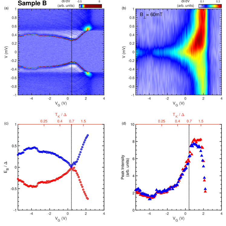
Following the same headlines as in sample A, the characterization of sample B starts with the measurement of a linear shunt resistance of 15 M at V, deep in the even diamond. Values for the superconducting pairing energy of the probing ( eV) and the strongly coupled lead ( eV) have been extracted from the differential conductance map in the S state (Fig. S10a) following the same criteria as in sample A. Such an increase of the superconducting gap size in thin aluminum films with respect to the usual bulk value has been previously reported and explained as a consequence of confinement effects and granularity, Court et al. (2007); Levy-Bertrand et al. (2019); Shanenko et al. (2008) and has been commonly observed in several of our \ceAl electromigration junctions. A more stable gate enables us to map the sample over a larger range of . For instance, the conductance map in the N state (Fig. S10b) shows the zero-bias Kondo resonance developing at the degeneracy point of the quantum dot (situated at V) and reaching a minimum intensity at V, indicating the center of the odd diamond, and corresponding to the maximum of the YSR states’ energy dispersion in the -phase. The complete concealment of the less intense diamond edges, buried below the Kondo-enhanced ones, makes the analysis of the diamond features and the extraction of impossible in this sample.
According to the results obtained for the Kondo energy scale extraction in sample A, we give an experimental definition of as the FWHM/2.9 of the Kondo resonance, this time subtracting the differential conductance background, taken as the average conductance measured between V = to mV. By extracting the YSR states’ energies and replacing axis with the corresponding non-dimensionalized with the extracted , we find the occurrence of the phase transition at (Fig. S10c), analogous to sample A. This result points toward a similar ratio of in this sample, which is not striking since we employed the same nano-particles colloidal solution in the fabrication of both samples, displaying a small size-distribution 10 % (leading to similar values). The nano-particles functionalizing ligands (dodecanethiol) may pose a limit for the minimum distance between the nano-particle and the lead, or in other words, the tunnel coupling . A relatively higher Kondo-enhanced diamond edge w.r.t. the zero-bias resonance, together with a sharp decrease of the YSR peak intensity across the phase transition (Fig. S10d) may point towards a larger tunnel coupling of the quantum dot to the probing electrode, becoming more sensitive to differences in the refilling rate at both sides of the phase transition.
Faint resonances displaying the same energy dispersion and dependence of the YSR peaks can be observed in Fig. S10a at higher energies, appearing both inside the spectroscopic gap and also merging into the quasi-particle continuum. A hypothetical spiky density of states above in the probing lead (maybe caused by nanostructuration and granularity of the \ceAl at the constriction) can result in low intensity replicas of the YSR resonances at higher energies.