Tailoring optical and magnetic properties of molybdenum disulphide nanosheets by incorporating plasmonic gold nanoparticles
Abstract
Abstract: The present paper deals with the systematic growth of plasmonic gold nanoparticles (Au NPs) on molybdenum disulphide (MoS2) nanosheets as well as the effect of Au NPs on the optical and magnetic properties. The crystalline nature of the nanocomposites is confirmed by X-ray diffraction and transmission electron microscopic techniques. The optical properties are characterized using absorption and Raman spectroscopic techniques. The electron paramagnetic resonance technique is used to study the magnetic response of the nanocomposites. The paper attempts to gain a fundamental understanding of the two-dimensional nanomaterial-based composites for their applications in the magnetic and optical devices.
I Introduction
In recent years, transition metal dichalcogenides (TMDs) have gained significant interest due to their vast applications in the field of energy transfer, catalysis, optical and electronic devices.Goodfellow et al. (2016); Prins, Goodman, and Tisdale (2014); Latorre-Sánchez et al. (2015); Wang et al. (2012); Wu et al. (2018); Patel et al. (2017); Rani et al. (2019) Among these TMD materials, molybdenum disulphide (MoS2) and tungsten disulphide (WS2) have been explored as various semiconducting devices. The bulk TMDs generally comprise many layers of nanosheets. The weak van der Waals interaction in the inter-layer of TMDs binds them to form bulk materials. The optical and electrical properties of TMDs strongly depend on the number of layers. The TMDs have a band gap that is dependent on the number of layers. In bulk form, they have indirect band gap while in case of monolayer, a direct band gap is observed.Mak et al. (2010) The transition from indirect to direct band gap results in high photoluminescence from TMDs nanosheets.Chhowalla et al. (2013) Having a band gap in the visible region renders more usefulness of the TMDs nanosheets in opto-electronic devices as compared to graphene, where a zero band gap is observed.Meric et al. (2008) In the monolayer of TMDs there are three layers of atoms – a layer of transition metal (MoW) sandwiched between two layers of chalcogenides (SSe).Chakraborti et al. (2016) Thus, it forms a MX2 structure. In bulk form, MoS2 has 1.2 eV band gap while the monolayer has 1.9 eV band gap. Similarly, WS2 has 1.3 eV band gap in bulk and 2.1 eV in the single layer form.Lee et al. (2012); Chhowalla et al. (2013); Shakya et al. (2016) Owing to this characteristic, finite band gap MoS2 monolayer can complement the weakness of gapless graphene, making it a promising two dimensional (2D) material for next generation applications in switching and opto-electronic devices. Thus, MoS2 finds its applications in diverse fields like sensors, energy storage in lithium-ion batteries, opto-electronic devices, flexible electronic devices, photoluminescence, valleytronics and field-effect transistors.Zhu et al. (2013); Chen et al. (2017); Song et al. (2016); Zibouche et al. (2014); Bang et al. (2014) MoS2 has also been explored as catalyst for hydrodesulphurization and hydrogen evolution in recent years.Lukowski et al. (2013); Luo et al. (2018); Paredes et al. (2016); Lee et al. (2013) Atomically-thin MoS2 sheets have relatively large in-plane mobility and mechanical stability.
The physical and chemical properties of MoS2 nanosheets can be manifested many fold by incorporating noble metal nanoparticles. Hence, nanocomposites can be used in a vast area of applications. Among noble metal nanoparticles, gold (Au) nanoparticles have an advantage due to its non-toxic nature and excellent stability. Further, Au is known to have a strong affinity for sulphur, which has been exploited to enhance charge transportation along interplanar directions and act as spacers to inhibit re-stacking of the TMDs. Recently, various research groups have synthesized and used Au-MoS2 nanocomposites in photocatalysis, surface enhanced Raman scattering and photovoltaic applications. Few research groups have also worked in the field of synthesis of Au NPs decorated on MoS2 sheets and its applications as hydrogen catalysis, Fermi level engineering, photoluminescence quenching, etc.Song et al. (2016); Chen et al. (2017); Zibouche et al. (2014)
There are various studies on the optical and electrical properties of metal based MoS2 nanosheets.Miao et al. (2015); Su et al. (2015); Li et al. (2017); Kaushik et al. (2014) Besides, there are a few reports on the magnetic properties of metal based two dimensional nanosheets, especially the electron paramagnetic resonance (EPR) studies. In the present paper, we report chemical exfoliation of MoS2 nanosheets for spontaneous decoration of Au NPs on MoS2 sheets. A direct redox reaction is done with a gold precursor chloroauric acid (HAuCl4) and sodium dodecyl benzene sulfonate as the stabilizing agent. The Au NPs are successfully deposited on chemically exfoliated sheets. The optical and magnetic properties of the nanocomposites are then explored using optical spectroscopic techniques and EPR spectroscopy.
II Experimental methods
II.1 Materials
Molybdenum disulphide (MoS2) powder, N-Methyl 2-pyrrolidone (NMP), Isopropyl alcohol (IPA), Hydrogen tetrachloroaurate trihydrate (HAuCl4.3H2O), Sodium dodecyl benzene sulfonate (SDBS) were obtained from Sigma Aldrich. All the chemicals were used without further purification.
II.2 Chemical exfoliation of MoS2 nanosheets
MoS2 nanosheets have been synthesized via liquid phase exfoliation method. For the synthesis of MoS2 nanosheets, 0.05g of bulk MoS2 powder was dispersed in 20 mL of NMP, IPA and distilled water (volume ratio 3:1:1) mixed solvent. The solution was ultrasonicated continuously for 24 hours at room temperature. After 24 hours of sonication the colour of solution changed from dark greyish black to greenish. The resultant green dispersion obtained was retained for 30 min for settling down the un-exfoliated MoS2. The clear supernatant was collected and 10 mg of SDBS was added to it. The resultant solution was then allowed to settle down in the next 30 min.
II.3 Synthesis of Au-MoS2 nanocomposites
For the synthesis of Au-MoS2 nanocomposites, stock solution of 10 mM Au salt (HAuCl4.3H2O) was prepared. Four sets each of 2 mL dispersion of exfoliated MoS2 nanosheets were taken for the further synthesis of Au-MoS2 nanocomposites. In these four sets, different quantities of Au salt solution (2L, 4L, 6L and 8L) were added and the mixtures were kept for aging for 48 hours.
II.4 Characterization techniques
The physical properties of MoS2 and Au-MoS2 nanocomposites were characterized by using spectroscopic and microscopic techniques. The morphology of the nanomaterial was investigated using transmission electron microscopy (TEM). The TEM analysis of MoS2 and Au-MoS2 nanocomposites was done using JEOL 2100F transmission electron microscope operated at 200 kV. The crystallinity of MoS2 and Au-MoS2 nanocomposites was explored using X-ray diffractometer from PANalytical with Cu K (0.15 nm) as X-ray source. The Raman spectra of MoS2 and Au-MoS2 nanocomposites were recorded by a confocal Raman microscope with an excitation source as 532 nm laser. The absorption spectra of MoS2 and Au-MoS2 were recorded using UV-Vis absorption spectrophotometer (Labtronics, LT-2700, India). The EPR spectra were obtained at room temperature using EPR spectrometer (Bruker, EMX MicroX).
III Results and discussion
III.1 TEM
The shape and size of MoS2 and that of Au NPs on the MoS2 nanosheets were investigated using transmission electron microscopy (TEM) set-up. The TEM images of MoS2 and Au-MoS2 nanosheets are shown in Fig. 1.
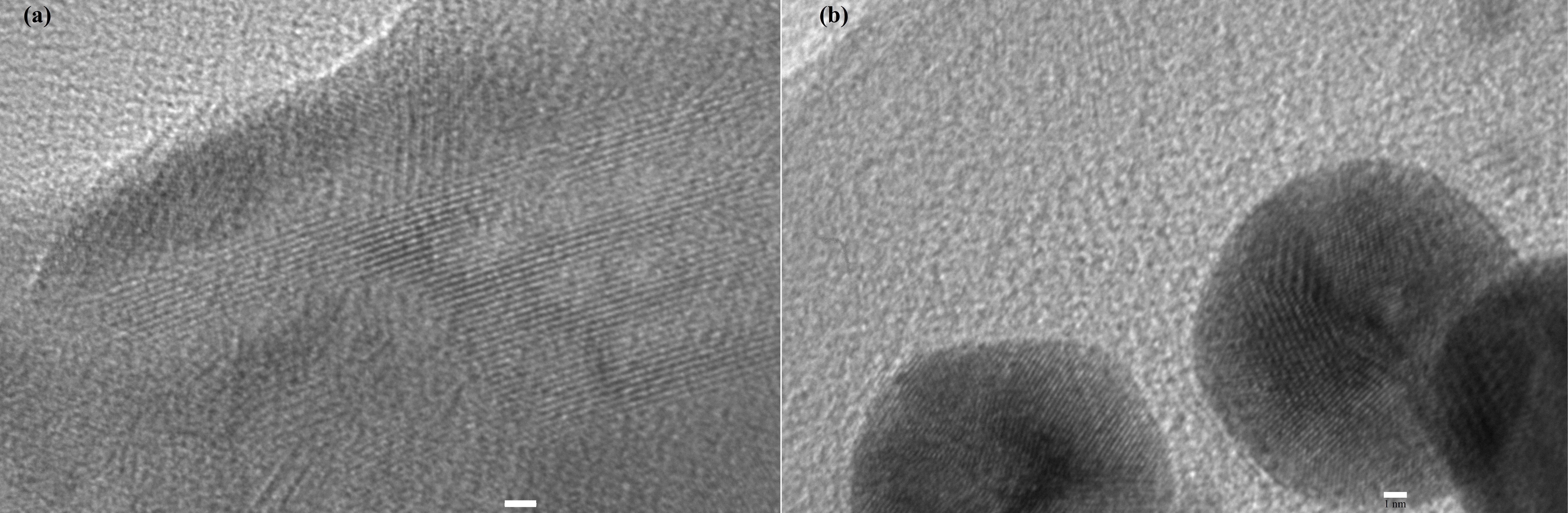
In the Fig. 1(a) sheet-like structure is observed, which corresponds to exfoliated MoS2. In MoS2, the lattice spacing is of the order of 0.27 nm, which corresponds to (100) plane.Luo et al. (2016) In case of Au-MoS2, the Au NPs are found to be of spherical shape and size of these particles is around 20 nm (Fig. 1(b)). The lattice plane spacing in the Au NPs corresponding to FCC lattice of Au is observed and spacing is of the order of 0.22 nm, which corresponds to (111) plane of gold lattice.Lin et al. (2008)
III.2 XRD
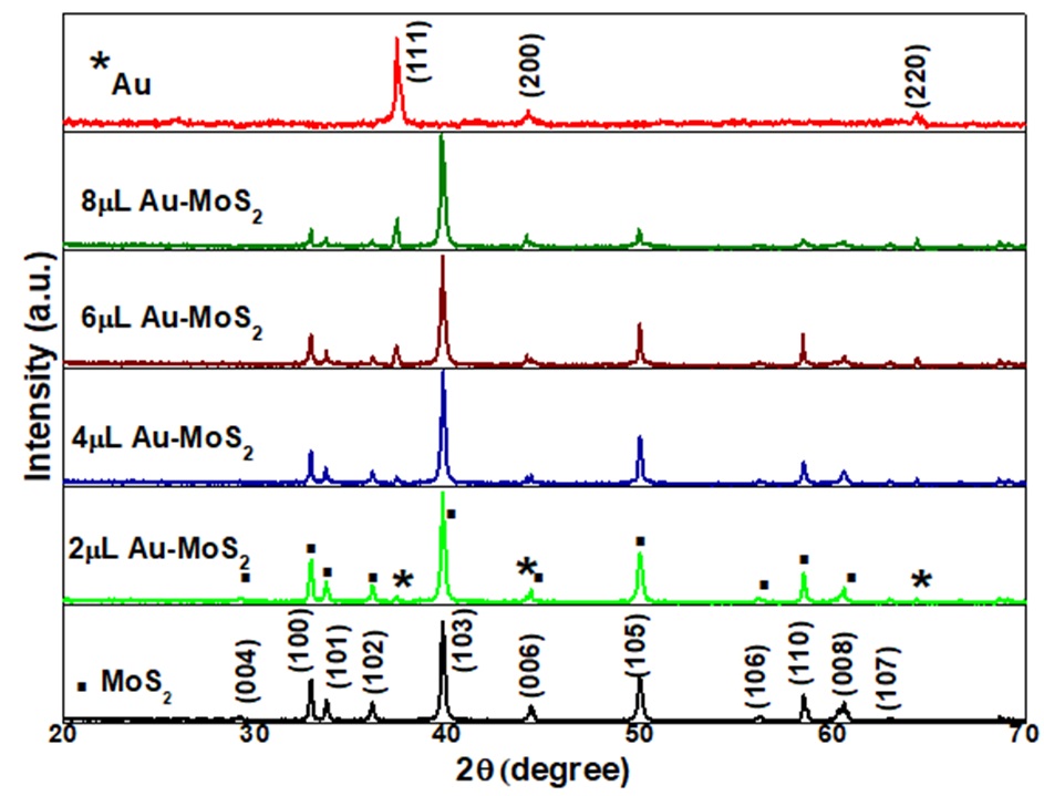
The XRD technique was used for investigating the crystal structure and lattice planes of the Au NPs and MoS2 nanosheets. The XRD patterns of pristine Au and MoS2 along with the Au-MoS2 nanocomposites are shown in Fig. 2. In these XRD patterns, the diffraction peaks at 29.19∘, 32.88∘, 33.68∘, 36.09∘, 39.75∘, 44.34∘, 49.99∘, 56.19∘, 58.50∘, 60.61∘ and 62.95∘ are observed that are attributed to lattice planes (004), (100), (101), (102), (103), (006), (105), (106), (110), (008) and (107) of MoS2, respectively (JCPDS No. 37-1492).Xu et al. (2015) After Au NPs decoration, the Au-MoS2 shows additional diffraction peaks at 37.34∘, 44.17∘ and 64.40∘ corresponding to the (111) (200) and (220) planes, respectively, of Au phase (JCPDS No. 04-0784),Jiang et al. (2012) that indicates FCC Au NPs have been successfully decorated on the MoS2 surface. Intensity of the peaks corresponding to Au enhances as the concentration of Au increases in the nanocomposites, while the peaks of MoS2 decrease correspondingly, which is clearly observed in Fig. 2. Lowering in diffraction intensity is due to decrease in the exposure area of MoS2 nanosheets in presence of Au NPs. The presence of Au NPs hinders the exposure area of the MoS2.
III.3 Raman study
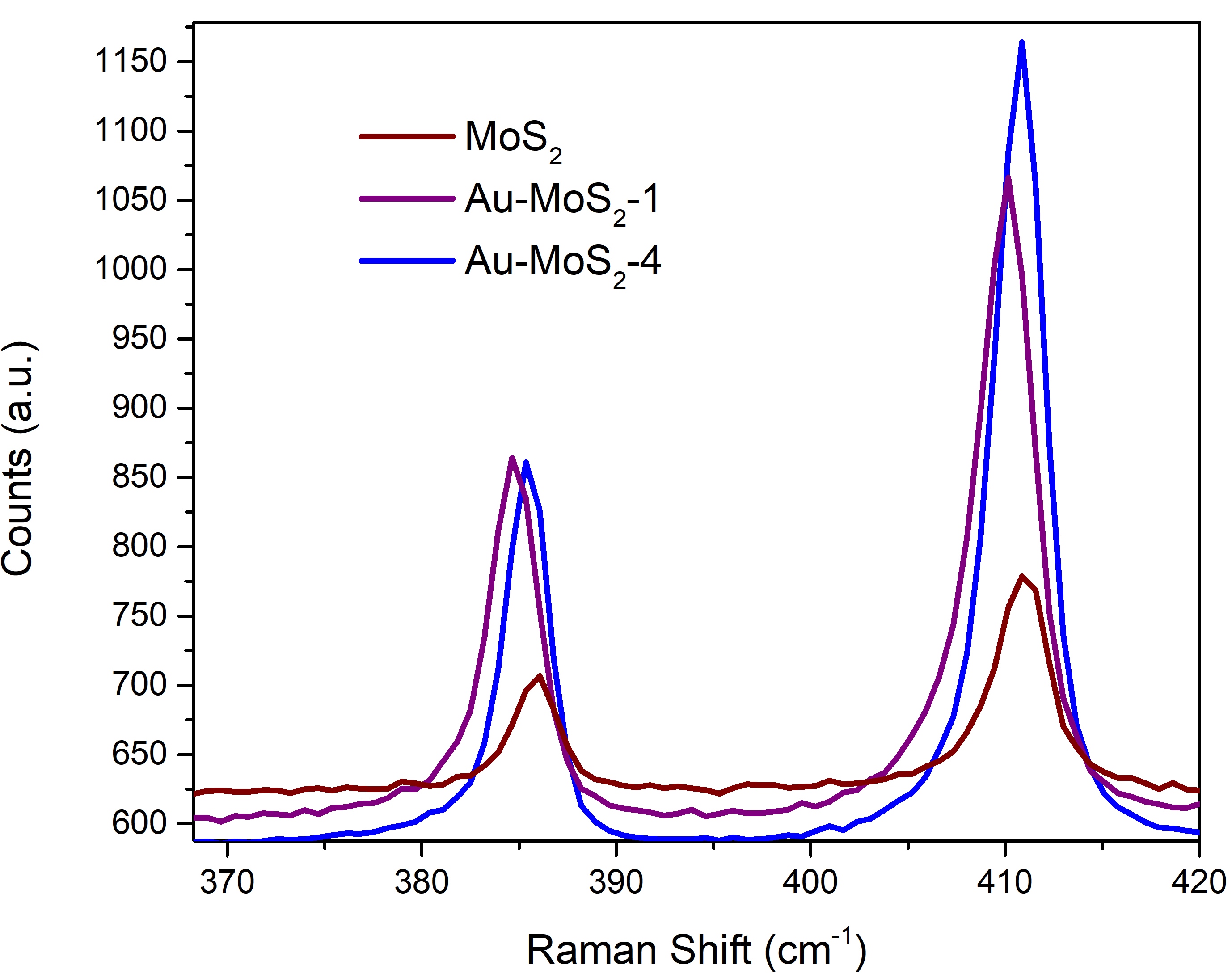
The vibrational modes of MoS2 nanosheets and the effect of Au NPs on them were investigated using Raman spectrometer. The Raman spectra of MoS2 and Au-MoS2 nanosheets are shown in Fig. 3. The Raman spectra exhibit two distinct Raman peaks – one around 385.9 cm-1 and the other around 410.9 cm-1. These peaks are associated with E and A1g modes of MoS2, respectively.Shakya et al. (2016) The E mode is attributed to the in-plane vibration of Mo and S atoms and this mode is sensitive to the built-in strain of 2D MoS2. The A1g mode is related to the out-of-plane vibration of S atoms, which is a reflection of the interlayer van der Waals interaction. For Au-MoS2, red shift in the E and A1g modes are observed. The shifting is attributed to the effect of lattice strain due to the curvature of MoS2 shell. The frequency difference of the E and A1g peaks comes out to be about 25 cm-1 that renders exfoliation of few-layers MoS2 sheets.Plechinger et al. (2012) In the presence of Au NPs, the intensity of Raman peaks are also enhanced. The enhancement is due to the plasmonic effect of Au NPs. The presence of Au NPs causes enhanced electric field near the surface of Au NPs and hence the intensity of Raman signal is enhanced. This contribution is due to the effect of localized surface plasmon resonance (LSPR) of Au nanoparticle cores, typically called surface enhanced Raman scattering (SERS).Su et al. (2014)
III.4 UV-Vis absorption
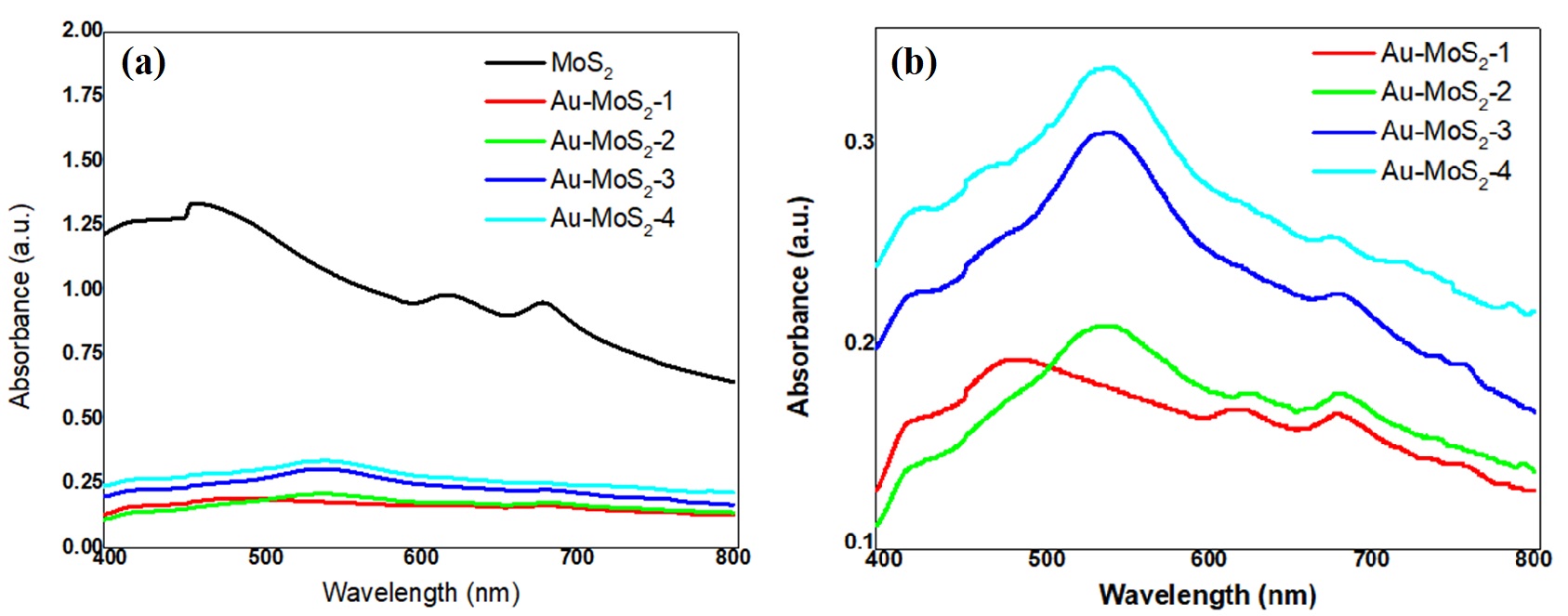
The optical absorption of pristine MoS2 nanosheets and Au-MoS2 nanocomposites has been explored using UV-Vis absorption spectrophotometer. The absorption spectra of MoS2 and Au-MoS2 are shown in Fig. 4. The absorption spectrum of MoS2 nanosheet shows two small humps in the visible range – one at 620 nm and other at 670 nm, which are known as B and A excitonic peaks, respectively.Patel et al. (2017) These peaks arise due to spin-orbit interaction causing splitting of valence band energy levels and the excitonic transitions between the splitted valence bands and the minima of conduction band at the -point of Brillouin zone. The interlayer coupling also plays an important role in the valence band splitting. When a small aliquot of gold precursor was added into chemically exfoliated MoS2, a new absorption peak corresponding to the Au plasmon band at around 530 nm emerged, suggesting the consumption of Au3+ and formation of gold nanoparticles.Mustafa et al. (2010) As we increase the Au concentration, the surface plasmon resonance peaks of Au experiences both red shift and increase in the intensity of peaks (shown in Fig.4(b)). These shifting infer to strong plasmon-exciton coupling between Au and MoS2. The surface plasmon resonance strongly depends on shape, size and separation of the nanoparticles along with the surrounding environment.Amendola et al. (2017) In Fig. 4(b), it is observed that when the concentration of Au is low the SPR peak is not so prominent, which is due to smaller size of Au NPs. When these particles have size less then 2-3 nm, the localized plasmons are not observed. The extent of Au-ion reduction by the spontaneous redox reaction can be estimated by monitoring the absorption peak of Au3+ and quantifying the loading level of Au on the surface of MoS2.
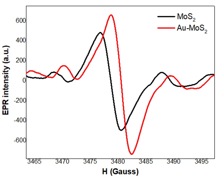
III.5 Electron paramagnetic resonance study
The paramagnetic properties of MoS2 and Au-MoS2 nanosheets are studied using electron paramagnetic resonance (EPR) spectroscopy. The EPR spectra of MoS2 and Au-MoS2 nanosheets are shown in Fig. 5. The EPR spectra originated due to the Mo−S dangling bonds, which are associated with different kinds of defects present in the MoS2 structure. The signature of the Mo−S dangling bonds can be detected as EPR absorbance around 3500 G of magnetic field and the intensity of the EPR peak is proportional to the concentration of Mo−S dangling bonds from the S-vacancies in the MoS2 structure.Cai et al. (2015) In case of pristine MoS2, an EPR signal at 3476 G is observed, which shows that some defects are created during the chemical exfoliation process using an ultrasonication bath. In case of Au-MoS2 nanostructures, a significant increase in the intensity as well as slight shift in the EPR peak is observed (3478 G), which is due to binding of Au with the sulphur atoms. The binding of Au-S leads to an overall increase in the sulphur vacant sites.Cai et al. (2015) Any kind of localized defect in the MoS2 structure, such as edge dislocation or dangling bond, provides a paramagnetic Mo site, which is characterized by an anisotropic g-tensor in the EPR.
IV Conclusion
In summary, the Au-MoS2 nanocomposites have been synthesized by using chemical exfoliation and reduction method. Different characterizations revealed that these Au-MoS2 nanocomposites show strong response towards the optical wavelengths due to the presence of surface plasmons in the nanocomposites, which enhances the charge transportation between MoS2 nanosheets. The presence of plasmonic particles was found to alter the magnetic property of the nanocomposites. This study could be further extended to other plasmonic nanoparticles of different shape and size, and their effect on the optical and magnetic response on the 2D nanomaterials could also be explored.
Acknowledgment: AC is thankful to AIRF JNU for TEM, Raman and EPR measurements, and AC is also thankful to DST-PURSE for partial financial support. Authors are thankful to Mr. Praveen Mishra for his help.
References
- Goodfellow et al. (2016) K. M. Goodfellow, C. Chakraborty, K. Sowers, P. Waduge, M. Wanunu, T. Krauss, K. Driscoll, and A. N. Vamivakas, “Distance-dependent energy transfer between cdse/cds quantum dots and a two-dimensional semiconductor,” Applied Physics Letters 108, 021101 (2016).
- Prins, Goodman, and Tisdale (2014) F. Prins, A. J. Goodman, and W. A. Tisdale, “Reduced dielectric screening and enhanced energy transfer in single-and few-layer mos2,” Nano letters 14, 6087–6091 (2014).
- Latorre-Sánchez et al. (2015) M. Latorre-Sánchez, I. Esteve-Adell, A. Primo, and H. García, “Innovative preparation of mos2–graphene heterostructures based on alginate containing (nh4) 2mos4 and their photocatalytic activity for h2 generation,” Carbon 81, 587–596 (2015).
- Wang et al. (2012) Q. H. Wang, K. Kalantar-Zadeh, A. Kis, J. N. Coleman, and M. S. Strano, “Electronics and optoelectronics of two-dimensional transition metal dichalcogenides,” Nature nanotechnology 7, 699 (2012).
- Wu et al. (2018) F. Wu, Y. Xia, M. Sun, and A. Xie, “Two-dimensional (2d) few-layers ws2 nanosheets: An ideal nanomaterials with tunable electromagnetic absorption performance,” Applied Physics Letters 113, 052906 (2018).
- Patel et al. (2017) A. S. Patel, P. Mishra, P. K. Kanaujia, S. S. Husain, G. V. Prakash, and A. Chakraborti, “Investigating resonance energy transfer from protein molecules to van der waals nanosheets,” RSC Advances 7, 26250–26255 (2017).
- Rani et al. (2019) A. Rani, K. Singh, A. S. Patel, A. Chakraborti, S. Kumar, K. Ghosh, and P. Sharma, “Visible light driven photocatalysis of organic dyes using sno2 decorated mos2 nanocomposites,” Chemical Physics Letters , 136874 (2019).
- Mak et al. (2010) K. F. Mak, C. Lee, J. Hone, J. Shan, and T. F. Heinz, “Atomically thin mos 2: a new direct-gap semiconductor,” Physical review letters 105, 136805 (2010).
- Chhowalla et al. (2013) M. Chhowalla, H. S. Shin, G. Eda, L.-J. Li, K. P. Loh, and H. Zhang, “The chemistry of two-dimensional layered transition metal dichalcogenide nanosheets,” Nature chemistry 5, 263 (2013).
- Meric et al. (2008) I. Meric, N. Baklitskaya, P. Kim, and K. L. Shepard, “Rf performance of top-gated, zero-bandgap graphene field-effect transistors,” in 2008 IEEE International Electron Devices Meeting (IEEE, 2008) pp. 1–4.
- Chakraborti et al. (2016) A. Chakraborti, A. S. Patel, P. K. Kanaujia, P. Nath, G. V. Prakash, and D. Sanyal, “Resonance raman scattering and ab initio calculation of electron energy loss spectra of mos2 nanosheets,” Physics Letters A 380, 4057–4061 (2016).
- Lee et al. (2012) H. S. Lee, S.-W. Min, Y.-G. Chang, M. K. Park, T. Nam, H. Kim, J. H. Kim, S. Ryu, and S. Im, “Mos2 nanosheet phototransistors with thickness-modulated optical energy gap,” Nano letters 12, 3695–3700 (2012).
- Shakya et al. (2016) J. Shakya, A. S. Patel, F. Singh, and T. Mohanty, “Composition dependent fermi level shifting of au decorated mos2 nanosheets,” Applied Physics Letters 108, 013103 (2016).
- Zhu et al. (2013) C. Zhu, Z. Zeng, H. Li, F. Li, C. Fan, and H. Zhang, “Single-layer mos2-based nanoprobes for homogeneous detection of biomolecules,” Journal of the American Chemical Society 135, 5998–6001 (2013).
- Chen et al. (2017) B. Chen, E. Liu, T. Cao, F. He, C. Shi, C. He, L. Ma, Q. Li, J. Li, and N. Zhao, “Controllable graphene incorporation and defect engineering in mos2-tio2 based composites: towards high-performance lithium-ion batteries anode materials,” Nano Energy 33, 247–256 (2017).
- Song et al. (2016) W. G. Song, H.-J. Kwon, J. Park, J. Yeo, M. Kim, S. Park, S. Yun, K.-U. Kyung, C. P. Grigoropoulos, S. Kim, et al., “High-performance flexible multilayer mos2 transistors on solution-based polyimide substrates,” Advanced Functional Materials 26, 2426–2434 (2016).
- Zibouche et al. (2014) N. Zibouche, P. Philipsen, A. Kuc, and T. Heine, “Transition-metal dichalcogenide bilayers: Switching materials for spintronic and valleytronic applications,” Physical Review B 90, 125440 (2014).
- Bang et al. (2014) G. S. Bang, K. W. Nam, J. Y. Kim, J. Shin, J. W. Choi, and S.-Y. Choi, “Effective liquid-phase exfoliation and sodium ion battery application of mos2 nanosheets,” ACS applied materials & interfaces 6, 7084–7089 (2014).
- Lukowski et al. (2013) M. A. Lukowski, A. S. Daniel, F. Meng, A. Forticaux, L. Li, and S. Jin, “Enhanced hydrogen evolution catalysis from chemically exfoliated metallic mos2 nanosheets,” Journal of the American Chemical Society 135, 10274–10277 (2013).
- Luo et al. (2018) S. Luo, S. Dong, C. Lu, C. Yu, Y. Ou, L. Luo, J. Sun, and J. Sun, “Rational and green synthesis of novel two-dimensional ws2/mos2 heterojunction via direct exfoliation in ethanol-water targeting advanced visible-light-responsive photocatalytic performance,” Journal of colloid and interface science 513, 389–399 (2018).
- Paredes et al. (2016) J. I. Paredes, J. M. Munuera, S. Villar-Rodil, L. Guardia, M. Ayán-Varela, A. Pagán, S. D. Aznar-Cervantes, J. L. Cenis, A. Martínez-Alonso, and J. M. Tascón, “Impact of covalent functionalization on the aqueous processability, catalytic activity, and biocompatibility of chemically exfoliated mos2 nanosheets,” ACS applied materials & interfaces 8, 27974–27986 (2016).
- Lee et al. (2013) G.-H. Lee, Y.-J. Yu, X. Cui, N. Petrone, C.-H. Lee, M. S. Choi, D.-Y. Lee, C. Lee, W. J. Yoo, K. Watanabe, et al., “Flexible and transparent mos2 field-effect transistors on hexagonal boron nitride-graphene heterostructures,” ACS nano 7, 7931–7936 (2013).
- Miao et al. (2015) J. Miao, W. Hu, Y. Jing, W. Luo, L. Liao, A. Pan, S. Wu, J. Cheng, X. Chen, and W. Lu, “Surface plasmon-enhanced photodetection in few layer mos2 phototransistors with au nanostructure arrays,” Small 11, 2392–2398 (2015).
- Su et al. (2015) J. Su, N. Li, Y. Zhang, L. Feng, and Z. Liu, “Role of vacancies in tuning the electronic properties of au-mos2 contact,” AIP Advances 5, 077182 (2015).
- Li et al. (2017) Y. Li, J. G. DiStefano, A. A. Murthy, J. D. Cain, E. D. Hanson, Q. Li, F. C. Castro, X. Chen, and V. P. Dravid, “Superior plasmonic photodetectors based on au@ mos2 core–shell heterostructures,” ACS nano 11, 10321–10329 (2017).
- Kaushik et al. (2014) N. Kaushik, A. Nipane, F. Basheer, S. Dubey, S. Grover, M. M. Deshmukh, and S. Lodha, “Schottky barrier heights for au and pd contacts to mos2,” Applied Physics Letters 105, 113505 (2014).
- Luo et al. (2016) Y. Luo, D. Huang, M. Li, X. Xiao, W. Shi, M. Wang, J. Su, and Y. Shen, “Mos2 nanosheet decorated with trace loads of pt as highly active electrocatalyst for hydrogen evolution reaction,” Electrochimica Acta 219, 187–193 (2016).
- Lin et al. (2008) Z.-H. Lin, Y.-W. Lin, K.-H. Lee, and H.-T. Chang, “Selective growth of gold nanoparticles onto tellurium nanowires via a green chemical route,” Journal of Materials Chemistry 18, 2569–2572 (2008).
- Xu et al. (2015) M. Xu, F. Yi, Y. Niu, J. Xie, J. Hou, S. Liu, W. Hu, Y. Li, and C. M. Li, “Solvent-mediated directionally self-assembling mos 2 nanosheets into a novel worm-like structure and its application in sodium batteries,” Journal of Materials Chemistry A 3, 9932–9937 (2015).
- Jiang et al. (2012) Z. Jiang, Q. Zhang, C. Zong, B.-J. Liu, B. Ren, Z. Xie, and L. Zheng, “Cu–au alloy nanotubes with five-fold twinned structure and their application in surface-enhanced raman scattering,” Journal of Materials Chemistry 22, 18192–18197 (2012).
- Plechinger et al. (2012) G. Plechinger, S. Heydrich, J. Eroms, D. Weiss, C. Schüller, and T. Korn, “Raman spectroscopy of the interlayer shear mode in few-layer mos 2 flakes,” Applied Physics Letters 101, 101906 (2012).
- Su et al. (2014) S. Su, C. Zhang, L. Yuwen, J. Chao, X. Zuo, X. Liu, C. Song, C. Fan, and L. Wang, “Creating sers hot spots on mos2 nanosheets with in situ grown gold nanoparticles,” ACS applied materials & interfaces 6, 18735–18741 (2014).
- Mustafa et al. (2010) D. E. Mustafa, T. Yang, Z. Xuan, S. Chen, H. Tu, and A. Zhang, “Surface plasmon coupling effect of gold nanoparticles with different shape and size on conventional surface plasmon resonance signal,” Plasmonics 5, 221–231 (2010).
- Amendola et al. (2017) V. Amendola, R. Pilot, M. Frasconi, O. M. Marago, and M. A. Iati, “Surface plasmon resonance in gold nanoparticles: a review,” Journal of Physics: Condensed Matter 29, 203002 (2017).
- Li et al. (2019) L. Li, Z. Qin, L. Ries, S. Hong, T. Michel, J. Yang, C. Salameh, M. Bechelany, P. Miele, D. Kaplan, et al., “Role of sulfur vacancies and undercoordinated mo regions in mos2 nanosheets towards the evolution of hydrogen,” ACS nano (2019).
- Lu, Kummel, and Robertson (2018) H. Lu, A. Kummel, and J. Robertson, “Passivating the sulfur vacancy in monolayer mos2,” APL Materials 6, 066104 (2018).
- Santosh et al. (2014) K. Santosh, R. C. Longo, R. Addou, R. M. Wallace, and K. Cho, “Impact of intrinsic atomic defects on the electronic structure of mos2 monolayers,” Nanotechnology 25, 375703 (2014).
- Li et al. (2018) A. Li, J. Pan, Z. Yang, L. Zhou, X. Xiong, and F. Ouyang, “Charge and strain induced magnetism in monolayer mos2 with s vacancy,” Journal of Magnetism and Magnetic Materials 451, 520–525 (2018).
- Cai et al. (2015) L. Cai, J. He, Q. Liu, T. Yao, L. Chen, W. Yan, F. Hu, Y. Jiang, Y. Zhao, T. Hu, et al., “Vacancy-induced ferromagnetism of mos2 nanosheets,” Journal of the American Chemical Society 137, 2622–2627 (2015).