Automated discovery of superconducting circuits and its application to
4-local coupler design
Abstract
Superconducting circuits have emerged as a promising platform to build quantum processors. The challenge of designing a circuit is to compromise between realizing a set of performance metrics and reducing circuit complexity and noise sensitivity. At the same time, one needs to explore a large design space, and computational approaches often yield long simulation times. Here we automate the circuit design task using SCILLA, a software for automated discovery of superconducting circuits. SCILLA performs a parallelized, closed-loop optimization to design circuit diagrams that match pre-defined properties such as spectral features and noise sensitivities. We employ it to discover 4-local couplers for superconducting flux qubits and identify a circuit that outperforms an existing proposal with similar circuit structure in terms of coupling strength and noise resilience for experimentally accessible parameters. This work demonstrates how automated discovery can facilitate the design of complex circuit architectures for quantum information processing.
I Introduction
The promise of quantum computing to surpass the capabilities of classical computers relies on a robust and scalable underlying hardware architecture. In the context of quantum simulation and annealing, strong coupling, high connectivity, and many-body interactions between the qubits are necessary to accurately and efficiently represent the problem Hamiltonian Cao et al. (2015); Barkoutsos et al. (2017); Babbush et al. (2014). Superconducting circuits have proven to be a particularly well-suited platform due to their design versatility Krantz et al. (2019). Their quantum behavior arises from the interaction of modes that are set by effective inductances, capacitances, and non-linear Josephson junction elements in the circuit Vool and Devoret (2017). In this way, it is possible to design a wide variety of qubits and qubit-qubit coupling schemes at the circuit-diagram level and realize them in nanofabricated devices Krantz et al. (2019); Oliver and Welander (2013).
A largely unexplored approach to meet circuit design challenges is to use computational automated discovery. In other fields of science and engineering, automated discovery and inverse design have emerged as a solution to a variety of design problems. All of these problems share the task to identify a set of parameters for which a system of interest yields desired target properties. In contrast to forward design methods, where system properties are estimated from system parameters through direct measurements or computation, inferring the system parameters from target properties is a much more laborious process. Typical automated discovery workflows consist of proposing a set of system parameters and determining the resulting system properties. The similarity between the obtained system properties and the targeted properties is then used as a quantitative measure to refine the system parameters iteratively. Parameter refinements are usually implemented via various optimization procedures or reinforcement learning agents. In the physical sciences context, automated discovery has been applied to nanophotonic on-chip devices Lu and Vučković (2010); Piggott et al. (2015), complex quantum state generation in optical platforms Krenn et al. (2016); Melnikov et al. (2018), entanglement creation and removal in superconducting circuits Goerz et al. (2017), and further problems in many-body physics Chertkov and Clark (2018); Wigley et al. (2016) and chemistry Gómez-Bombarelli et al. (2018); Sumita et al. (2018); Zhavoronkov et al. (2019). This resulted in the discovery of conceptually new or previously unexplored solutions.
In the field of superconducting circuits, a contemporary design challenge is the implementation of many-body interactions. Such interactions of more than two qubits commonly appear in effective spin models of quantum chemistry, quantum error mitigation schemes, and advanced driver Hamiltonians for quantum annealing Babbush et al. (2014); Kandala et al. (2017); Bacon (2006); Fowler et al. (2012); Hen and Spedalieri (2016); Martoňák et al. (2004). Interactions involving qubits are called -local and comprise Pauli operations in the system Hamiltonian that act on qubits simultaneously. The interaction Hamiltonian has the form
where is the coupling strength and denotes the type of Pauli matrix acting on each qubit. Several implementations for 3- and 4-local couplers in superconducting circuits have been proposed. Hamiltonian gadgets use ancilla qubits to encode the desired interaction in the effective low-energy spectrum of the system Kempe et al. (2006); Chancellor et al. (2017). Alternatively, individual flux qubits can be coupled to a common coupler circuit that mediates the interaction via a tailored potential Kerman (2018); Schöndorf and Wilhelm (2018); Melanson et al. (2019). The modularity of the tailored-potential approach in particular is reminiscent of existing 2-local couplers and holds promise for practical implementation Harris et al. (2007); Weber et al. (2017). Further work is required, however, to find coupler circuits that operate in experimentally accessible parameter regimes, reduce flux noise sensitivity, and eliminate spurious couplings.
The automated discovery task is to find a superconducting circuit diagram that fulfills a set of desired properties. To this end, we introduce a method for superconducting circuit closed-loop automated discovery (SCILLA) and implement it in software. We present the parallelized, closed-loop workflow that has access to design algorithms (generators) and can be connected to different circuit evaluators. The method is applicable to a wide range of search problems involving spectral properties and noise sensitivities of galvanically connected superconducting circuits. We demonstrate the performance and flexibility of SCILLA on the well-studied example of capacitatively shunted flux qubits Yan et al. (2016). We then highlight the competitive advantage of our approach by executing a discovery workflow which identifies noise-resilient 4-local coupling circuits. As stated above, such a coupler would constitute a valuable building block for future quantum simulators and quantum annealers.
II Methodology
The automated discovery workflow requires a circuit parameter generator, property evaluator, and merit estimator in order to fulfill a specified search task. In the following, it is shown how circuit search can be formulated as an optimization problem by taking the circuit parameters as an input list and calculating the resulting closeness to the target properties. We then describe the closed-loop implementation that handles parameter generation and optimization in a parallelized manner. Lastly, 4-local coupler design is reduced to a spectral engineering problem that is compatible with the automated discovery workflow.
Throughout this work, the properties of superconducting quantum circuits are calculated by constructing and diagonalizing the circuit Hamiltonian. For the automated discovery problem, and for spectral engineering problems more generally, the eigenenergies need to be calculated as a function of external degrees of freedom such as flux or charge offsets. Circuit quantization has been discussed extensively in previous work, treating the circuit as a network of lumped elements with canonically conjugate flux and charge variables Burkard et al. (2004); Girvin (2011); Vool and Devoret (2017); Krantz et al. (2019). We automatically determine the Hamiltonian of a broad class of circuits and solve it efficiently by choosing a mixed representation in the charge and harmonic oscillator bases Kerman (2018); Note (1).
II.1 Circuit design as an optimization problem
Automated discovery of circuits requires a quantitative metric to assess closeness of a candidate circuit to the target. While the target can take a wide variety of forms, in this work we discuss and illustrate the practicality of optimizing specifically towards spectral properties, symmetry in the circuit network, and flux noise sensitivity. It is straightforward to include more circuit properties as long as they can be obtained from Hamiltonian simulations in reasonable simulation time. In addition, multiple target properties can be combined in a unifying merit function for more balanced design procedures. We define the merit function as , taking the circuit parameters as an input list and returning a scalar value. It is defined such that a smaller function value corresponds to a circuit that better fulfills the target. The specific functional form of depends on the search task and needs to be carefully engineered for the optimization procedure to balance improvement of the sub-targets evenly. It will be defined explicitly for each task in Sec. III. Since the target properties in general depend on the results of Hamiltonian circuit simulations, it is assumed that has access to the simulation results for the input circuit.
The input contains an ordered list of the capacitance, inductance, and junction energy for each circuit element between each pair of nodes. If there is no circuit element between two nodes, the respective parameter value is zero. Therefore, the ordered list of circuit element parameters fully defines the circuit network and is used to construct the circuit Hamiltonian. The input also contains a list of external flux values – one for each inductive loop in the circuit. Each flux may only take the values or , ensuring a symmetric spectrum as required for the applications presented in Sec. III. The circuit parameters are bounded, following typical experimentally accessible values Weber et al. (2017); Oliver and Welander (2013): up to for capacitances and up to for inductances. The lower bound for inductances is chosen as in the 4-local coupler discovery in Sec. III.2. This ensures that each inductor is large enough for qubits to couple mutually inductively to it. For Josephson junction energies, we allow a range of for the flux qubit benchmark in Sec. III.1 and for the 4-local coupler discovery. The latter provides more design flexibility and corresponds to junctions with critical current density, junction width and junction length. The intrinsic parallel capacitance of each Josephson junction depends on its respective physical geometry and is implicitly assumed. Throughout this work, we denote the Josephson junction energy, capacitance, or inductance of a circuit element between two nodes and by , , and , respectively.
In addition to the constraints on parameter values, we identify rules for the placement of components in the circuit network. Capacitative elements may be placed in parallel to inductive elements such as junctions and inductors, i.e. between the same two nodes. However, parallel placement of an inductance and a junction is not allowed to prevent the increased circuit complexity resulting from additional inductive loops formed in this way. The degree of connectivity, i.e. the number of connections that each node has to other nodes, is set by the non-zero parameters in the input . A circuit with more nodes and higher connectivity allows for more complex spectral engineering in reaching the target. However, it is disadvantageous to increase the circuit size beyond the requirement of the objective. Larger circuits may demand more calibration and more control hardware in experiments. In addition, a larger number of external flux degrees of freedom usually leads to a greater flux noise susceptibility. In the case of two- and three-node circuits – excluding the ground node – as discussed in this work, the circuit network is planar even for all-to-all connection between the nodes. When moving to larger circuits, however, one needs to constrain certain circuit components to zero in order to maintain network planarity and thus ensure realizability in a planar on-chip architecture. In principle, circuit complexity and experimental feasibility can also be added to the target with a suitable merit evaluation.
II.2 Realizing closed-loop circuit discovery
SCILLA is a closed-loop implementation for accelerated computational circuit discovery available on GitHub 111The automated discovery implementation for use with a generic circuit simulator (not provided) is available at the following address: https://github.com/aspuru-guzik-group/scilla. The procedure autonomously searches the circuit space defined in Sec. II.1 for circuit architectures satisfying desired target properties. Similar approaches have already been successfully applied in the context of autonomous discovery and experimentation in chemistry and materials science Roch et al. (2018a, b). SCILLA contains a general-purpose method to compute properties of superconducting circuits Note (1). It is thus applicable to a wide range of circuit design applications.
The typical workflow in the closed-loop implementation of SCILLA is illustrated in Fig. 1. Each circuit search is started from a set of general instructions, which inform SCILLA about the size of the circuit and the number of components (see Fig. 1a). With these specifications, a design algorithm chooses the kinds of components to be placed at particular locations in the circuit graph, as well as component-specific parameters (see Fig. 1b). Then, properties of interest are computed for each designed circuit (see Fig. 1c). As the calculation of circuit properties is typically the most time consuming step of this workflow, SCILLA computes only the properties which are requested in the general instructions. SCILLA supports the computation of circuit spectra as well as estimations of the flux and charge noise sensitivites. The computed circuit properties are then used to evaluate the merit , determining how well a given circuit matches the desired target specifications (see Fig. 1d). Finally, the circuit composition which best satisfies the desired targets is determined (see Fig. 1e). The crucial element to “close the loop” – and thus enable autonomous circuit discovery – is to report the merit of a proposed circuit architecture to the design algorithm. Based on the feedback, the design algorithm can propose refined circuit architectures with improved target properties. Some design tasks require higher-level operations, such as computing a gradient during circuit design or probing the flux sensitivity of a considered circuit only if a predefined condition is met. Therefore, both the circuit design algorithms as well as the circuit merit evaluators are equipped with the capability to define new circuit evaluation tasks. Circuit evaluations requested during circuit design are prioritized to assure that individual circuit design tasks are completed quickly.
The workflow presented in Fig. 1 can be parallelized with little computational overhead by separating each step of the workflow into independent units (modules). Information about individual circuits, such as component parameters or circuit properties, are dynamically stored in a system of databases built on the SQLite database engine. The database implementation is the key component which allows the software to decouple each of the steps in the workflow and execute them individually. Details on the implementation are provided in the supplementary information (see Sec. S.1). The implicit parallelization of individual modules maximizes the number of circuits evaluated in parallel and thus utilizes available computing resources to higher capacity. Moreover, circuit properties can be computed asynchronously, which is crucial as the computational time required to evaluate a given circuit often depends on its component configuration and parameter values. With the implemented database system, all circuit parameters and properties which have been proposed and evaluated during the closed-loop sampling procedure are easily accessible. As data is stored in a standardized format, profound post-process analysis of the circuits is possible and has the potential to identify general principles for circuit design, which will be demonstrated in the results (see Sec. III).
The design modules within SCILLA can efficiently search the space of small circuits with relatively few components that can be evaluated quickly, as well as larger circuits with more components for which property calculations are more time consuming. As the hardness of the optimization depends on the search space size and merit definition, a number of different design strategies are implemented in the closed loop, ranging from random search strategies Bergstra and Bengio (2012); Bergstra et al. (2011) for coarse, massively parallelizable sampling over gradient-based methods Liu and Nocedal (1989); Morales and Nocedal (2011) to evolutionary strategies Shi and Eberhart (1998); Eberhart and Kennedy (1995); Miranda et al. (2018). A more detailed description of the supported methods is provided in the supplementary information (see Sec. S.1).
The closed-loop framework also enables the implementation of multi-step workflows. The user declares a search procedure based on a chosen design algorithm, can define analyses on the circuits sampled during this first search, and then trigger another circuit design round, for instance, to refine the previous search. Arbitrary combinations of different design and analysis steps are possible and can be easily integrated into the desired multi-step workflow. Examples of such workflows are provided in the circuit discovery applications presented in Sec. III as well as in the supplementary information (see Sec. S.2).
II.3 4-local interaction as a spectral engineering problem
The main application of SCILLA presented in this work is the discovery of 4-local couplers for superconducting flux qubits. We identify the key spectral property of such a coupler that yields the desired interaction when four flux qubits are coupled to its external flux degree of freedom via mutual inductance (see Fig. 2): a double-well profile of the coupler ground state energy versus external flux Kerman (2018). We note that this double-well flux spectrum of the coupler should not be confused with the inductive double-well potential of the flux qubit. The ground state and excited state of each flux qubit are given by persistent left- and right-circulating currents in the qubit loop, respectively. The circulating current change associated with the excitation (relaxation) of any of the flux qubits will shift the flux bias point of the coupler by a small flux offset (). It is assumed that all four flux qubits are identical, have no pair-wise coupling, and have the same interaction strength with the coupler. If the double-well profile of the coupler spectrum has flux spacings between energy values differing by as indicated in Fig. 2(b), then each qubit transition will raise or lower the potential energy of the system by . Applying external flux such that is biased at the center peak, the system energy separates into two energy manifolds associated with the parity of the qubit excitation number. This is equivalent to the coupler providing a 4-local interaction term . The challenge of engineering a 4-local coupler therefore becomes that of finding a circuit with the described double-well spectrum in a narrow flux range under realistic parameter constraints. In order to preserve quantum coherence, it is important to limit sensitivity to sources of noise, particularly flux noise if there are additional flux degrees of freedom in the coupler circuit Gustavsson et al. (2011); Krantz et al. (2019). After a circuit fulfilling these properties has been found, simulations of the full system including all four qubits and the coupler need to be performed in order to confirm the validity of the 4-local coupling mechanism presented above.
III Results & Discussion
We present the results of two circuit discovery instances. First, SCILLA is applied to a well-studied flux qubit example, testing the key features of the closed-loop implementation. Knowledge of the optimal solution enables us to study the performance of the closed-loop algorithm in reaching the target. Second, circuit discovery of 4-local couplers is performed. The best circuit identified by the software is analyzed to elucidate its underlying operational mechanism, derive general design principles, and show its promise for experimental implementation.
III.1 Benchmarking SCILLA by flux qubit discovery
As a benchmark for the automated discovery software, we define the target to be a capacitatively shunted (C-shunt) flux qubit. This is a design variant of the flux qubit that has been shown to yield improved reproducibility and coherence for quantum information processing applications Orlando et al. (1999); You et al. (2007); Yan et al. (2016). It is particularly well suited for strong qubit-qubit coupling in the quantum simulation and annealing context Weber et al. (2017). The circuit is given by a loop of two identical, large junctions and one smaller junction, with the small junction shunted by a large capacitance. It can be represented by a two-node circuit as shown in Fig. 3(a), with the additional bottom node declared ground. The following Josephson junction energies and capacitances are typical for this type of qubit and are chosen as the target parameters:
The intrinsic parallel capacitance of each junction is added to the listed capacitances.
The simulated transition energies between the ground state and the first – and second – excited states as a function of external flux through the circuit loop are shown in Fig. 3(b). This energy spectrum is defined as the first target property for the circuit search problem. There is, however, a continuous family of two-node circuits that fulfills this spectrum. The degeneracy is lifted by adding the requirement that the circuit is symmetric, i.e. that the component parameter values are close to , respectively. Rather than enforcing a constraint a priori, circuit symmetry is added as a second target. In this way, the design task tests a case of multi-objective search. In addition, symmetry in the circuit diagram is a practically relevant property that can often be translated to the chip design, limiting noise-inducing effects such as currents in the ground plane. It can be advantageous to have symmetry as a target property, rather than a constraint, such that it is only enforced when the other properties can be fulfilled at the same time. A single scalar merit function is constructed from a combination of the spectrum sub-merit and the symmetry sub-merit :
Here, and represent the candidate and target circuits’ transition energy from ground to th excited state as a function of external flux. The RMS deviation between these functions is evaluated over the period of one flux quantum and approximated numerically by computing the function values at discrete flux points. The parameters and are the upper bounds for the respective parameter values as defined in Sec. II.1. The weighing of the sub-merits is chosen such that their values are on the same order for a typical random circuit, and the logarithmic scaling was observed to improve optimizer performance. Therefore, the merit function is constructed by starting from a scalar form that allows for individual sub-merit optimization and then empirically choosing weighting and scaling parameters.
The workflow specified in the circuit searcher starts with random sampling from the parameter space, followed by gradient-based optimization with the L-BFGS-B algorithm Liu and Nocedal (1989); Morales and Nocedal (2011). Ten such search jobs are executed independently for greater throughput, each with 10 parallelized random samples and subsequent gradient-based refinement. The parameter space for the benchmark is six-dimensional and consists of the junction energies and capacitances shown in Fig. 3. No external flux needs to be specified, because the sole flux degree of freedom is varied to calculate the transition energy spectrum. Moreover, the Hamiltonian of general two-node circuits without linear inductances takes a simple form than does not require the general Hamiltonian construction procedure included in SCILLA. An optimized simulator for such two-node circuits is provided as a separate module and used here. The simplified Hamiltonian is provided in Sec. S.3 and a detailed implementation of the benchmark workflow is reported in Sec. S.2.
The result of 40 parallel circuit optimizations is shown in Fig. 3(c), which represents a subset of four of the ten independent search jobs. A fraction of of the runs (4 of 40) reach close to the global minimum defined by the target circuit. High accuracy in both the spectral and the symmetry sub-targets is achieved in the yellow-shaded area in the plot, which is reached after 30-60 optimizer iterations for the successful runs. The final spectrum of one successful run (circuit A) is shown in Fig. 3(b), matching the target spectrum accurately. Symmetry in circuit A is very high, the deviation between the parameters () and () being ().
The remaining refinement runs terminate at a higher merit value. Inspection of the final spectrum of one such run (circuit B) in Fig. 3(b) reveals that the spectrum is not close to the target. We identify the failure mechanism in that the merit function has local minima. In the surface projection of the merit function shown in Fig. 3(d), some local minima are visible as bright, yellow clusters around the global minimum. Since the gradient-based optimizer used for refinement is local, it will naturally terminate after reaching one of the local minima.
In summary, nearly all module types and functionalities of SCILLA have been tested in the benchmark. In particular, it is verified that circuit simulations and merit evaluations are executed in parallel and asynchronously as intended. The average run-time per search job is 6 h 41 min and evaluates circuits in total. Therefore, when including the computational overhead of the closed-loop software, the average simulation time of a circuit is . This compares well to in a typical single, isolated evaluation of a circuit on the same hardware. As a more general point about circuit discovery, we observe here that the optimization is non-convex even for a moderate search problem. A purely gradient-based optimizer is of limited use in this case, although the random starting point ensures that the optimum can be found in some trials. The success rate for finding good circuits is expected to decrease for larger circuits because of the increased parameter space dimensionality. The hardness of the search problem is also increased by more restrictive merit functions with more sub-merits. For the 4-local coupler search, the gradient-based optimizer is therefore replaced with an evolutionary strategy, which is able to avoid local minima. In addition, the available computational resources and parallelization capability of SCILLA are used to the maximum extent in order to explore a large portion of the design space and refine as many trial points as possible.
III.2 Noise-insensitive 4-local coupler discovery
We turn to the design challenge of coupler circuits for 4-local interaction of flux qubits. As detailed in Sec. II.3, this problem can be reduced to finding a circuit with a double-well ground state spectrum. The desired double-well profile is shown in Fig. 4(a), with the bias points for the 4-qubit excitation manifolds shown in red. The spacing between the wells and the peak needs to be small such that it can be bridged by the spin flip – and corresponding circulating current change – of a mutually inductively coupled flux qubit. Given the typical persistent currents and mutual inductances in strongly coupled flux qubit systems, we determine that the well-to-well spacing of the spectrum needs to be below Weber et al. (2017); Note (5). In addition to the spectral property, insensitivity to noise sources in the system is required. An often-observed effect of a flux offset in an additional inductive loop of the coupler circuit is shown as the gray trace in Fig. 4(a): The double-well spectrum tilts and becomes asymmetric, which would lead to unwanted, non-4-body terms in the interaction Hamiltonian. Therefore, the second objective is to mitigate such spectral shifts due to flux noise.
In order to write these targets in a unified merit function, several parameters of the double-well are determined. These parameters are visualized in Fig. 4(a) (dark red). In the computational routine, they are calculated in case a double-well feature is detected in a range around the bias point of the primary external flux of the circuit: First, the energy difference between the wells and the center peak determines the 4-local coupling strength and needs to be maximized. Second, the minimal energy difference between the ground and first excited state of the coupler is to be maximized; if it is too close to the qubits’ transition energy, the coupler can swap excitations with the qubits and break its operating principle of remaining in the ground state at all times. Third, asymmetry induced by flux offsets in the non-primary loops of the coupler is calculated as the energy difference between the minima of the left and right well. Flux noise is usually dominated by local two-level systems on the metal surface of the circuit, with a degree of flux noise correlation between loops that depends on the length of wire shared by them Koch et al. (2007); Gustavsson et al. (2011); Krantz et al. (2019). An upper bound on the effect of flux noise is determined by applying flux offsets individually to each non-primary flux degree of freedom and summing the resulting asymmetries . A scalar merit function combines the above parameters. It is given by the -norm of three terms that quantify the peak height, excited state splitting, and noise insensitivity targets.
The hyperparameters , specify the target values for peak height and excited state splitting. They serve as cut-off values for the respective parameters of the detected double-well as shown below. The noise sensitivity is determined as the ratio between the summed asymmetries and the peak height, and can assume a maximum value of 1.
The hyperparameters of the merit function are chosen empirically by trial of different hyperparameter sets. For the results presented in this work, they assume the values , , and . The merit function is constructed such that a joint optimization of two sub-merits is favored over individual optimization. The merit function assumes a minimum value of if all sub-merits are maximally satisfied. A merit of zero is assigned to the candidate circuit if no double-well is detected in the flux range around the bias point, the peak height is below , or the excited state splitting is below . In addition, a zero merit is assigned if the simulation fails, times out, or has large Hilbert space truncation errors. Therefore, circuits with little promise for successful optimization are effectively removed from the optimization workflow.
The workflow implemented in the circuit searcher applies insights from the flux qubit benchmark to the more complex task of coupler design with flexible circuit diagrams. It starts with random sampling of 15,000 circuits, which is about the limit beyond which database operations are observed to slow down. The best two of the 15,000 circuits are kept after filtering and are refined using the evolution-inspired swarm optimization module. Ten such jobs are executed independently for better utilization of the available computing resources. The random search space is chosen to span three-node circuits with connections between the nodes and to ground on which capacitances, junctions, and inductances can be placed. Under the constraints on placement of circuit components detailed in Sec. II.1, components are randomly assigned among the available positions. After sampling and filtering, the network configuration is fixed and only the component parameter values are refined. The configuration of the circuit network is therefore flexible, and the number of inductive loops varies between sampled circuits. This constitutes a consequential extension of the fixed-configuration, two-node search space that has been used for the benchmark, allowing for more degrees of freedom in reaching the 4-local coupler target. To calculate the properties of such circuits, the simulation module that implements the general-purpose circuit Hamiltonian simulation is used. The workflow implementation is described in more detail in Sec. S.2.
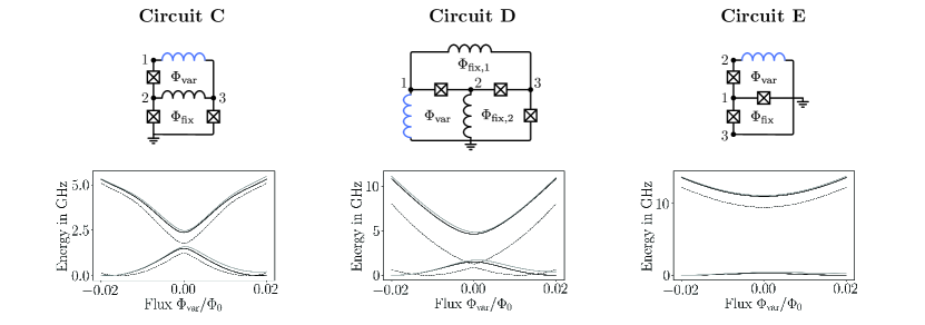
The results of the random search and subsequent swarm optimization are shown in Fig. 4(b). A double-well spectrum is detected in 7 of all 150,000 sampled circuits (). The swarm optimization improves the merit of all filtered circuits to varying degrees. The final best circuit, named circuit C hereafter, has the following properties after (before) refinement:
The circuit diagram is shown in the inset of Fig. 4(b). It is a two-loop circuit with the following non-zero component parameter values after refinement:
The double-well spectrum of circuit C emerges from the strong interaction of two rf SQUIDs at different flux bias points. The first SQUID is formed by the loop surrounding the external flux , which is biased at in the absence of qubits. The second rf SQUID loop encompasses the fixed external flux . For details on the derivation of the circuit C Hamiltonian, see supplementary Sec. S.5. We note that this computer-generated circuit has strong similarities with the 4-local coupler design proposed by Kerman Kerman (2018). The key differences are that the parameters are more easily accessible experimentally in our design and the two inductive loops are connected galvanically – and thus more strongly – than for mutual inductive coupling, allowing for a large double-well peak despite smaller loop currents. Moreover, the asymmetry relative to peak height arising from flux offsets is reduced by a factor of 3.3 in circuit C.
In total, 3 of the 7 double-well circuits from the automated discovery results have a similar layout as circuit C, with two inductive loops coupled through an inductance or junction. The remaining 4 circuits are three-loop circuits and therefore have two non-primary external flux degrees of freedom. In addition to circuit C, two more exemplary circuit optimization trajectories are highlighted in Fig. 4(b): circuits D and E. Circuit D is a three-loop circuit with 1.50 GHz double-well peak and 3.12 GHz excited state splitting. These desirable properties are, however, contrasted by an increased flux noise sensitivity due to the additional external flux in the third loop. Circuit E has two loops and a similar circuit network as circuit C but features a much larger excited state splitting of 10.8 GHz and much smaller double-well peak height of 0.24 GHz. The properties of circuits C, D, and E are listed in detail in Sec. S.4. These examplary search results show that the automated discovery workflow finds a variety of circuits that fulfill the double-well sub-merits to different degrees. It therefore supplies design options with different trade-offs, which can inform both theoretical understanding and practical implementation of the relevant class of circuits.
It remains to be demonstrated that circuit C in fact behaves as a 4-local coupler mediating an interaction , and thus that our reduction of the design problem to a spectral property is valid. For this reason, a full system simulation of four qubits coupled mutually inductively to the coupler as shown in Fig. 4(c) is performed. The energies of the 4-qubit excitation manifolds versus the qubit flux around degeneracy are shown in Fig. 4(d), illustrating how the states of different parities separate. A 4-local coupling strength of in the circulating current basis ( basis) of the qubits is extracted, which is lower than the double-well peak height used as a proxy for the coupling. Part of the reduction in coupling is caused by the flux points of the odd qubit excitation manifolds not lining up exactly with the minima of the double-well spectrum, as indicated conceptually by the red dots in Fig. 4(a). Further reduction mechanisms could include inductive loading of the coupler by the mutual inductive coupling to the qubits and interactions with the coupler’s excited state. Spurious terms of different locality, which are manifest as a splitting of states at the additional spectral crossing points in Fig. 4(d), are in the MHz-regime and thus negligible. We conclude that despite additional effects reducing the coupling, SCILLA applied to the double-well merit was able to design a coupler with several hundred MHz of 4-local coupling strength, even without performing costly full system simulations.
As predicted from the benchmark analysis, our success in finding a promising 4-coupler circuit rests on careful definition the merit function, choice of the discovery workflow, and exploitation of computational resources. Given the low success rate of sampling a circuit with double-well spectrum at all, a critical step has been to explore a large portion of the design space before attempting to refine promising circuits. Averaged over the ten batches, sampling 15,000 circuits took (). The subsequent swarm optimization with a total of 8,000 circuit evaluations in 200 iteration steps took an average of (). While the sampling time is relatively uniform, the swarm optimization runtime varies significantly with the circuit layout that is being optimized. In addition, it is observed that the simulation time per circuit is much longer in the swarm optimization, which is expected from the lower degree of parallelization, additional circuit simulations required by the merit evaluation, and larger number of database operations in the iterative optimization. On top of the runtimes of the sampling and optimization steps, the closed-loop procedure requires an additional that is mainly spent filtering the sampled circuits before swarm optimization. The filtering time is limited by the input/output operation speed of the used hardware and can be much lower on a different computing cluster.
Overall, SCILLA is able to accommodate the increased computational effort from adding a third node to the circuit and allowing for full flexibility for the circuit network. The added complexity is rewarded by successful fulfillment of the target properties. This warrants further study of improving the efficiencies of circuit simulation and search algorithms.
IV Conclusion
We demonstrated a computer-driven and highly parallelized approach to the design of superconducting circuits. We evaluated the performance of the developed method SCILLA and discovered circuits for design challenges with multiple objectives. Our results demonstrate that SCILLA is successful in finding new circuit architectures with superior performance than an existing proposal, namely a 4-local coupler with several hundred MHz of coupling strength, small unwanted coupling terms, small flux noise sensitivity, and experimentally accessible parameters. Given the modularity of the software implementation, it is straightforward to tackle new circuit design challenges that can be defined in terms of spectral properties and eigenstate expectation values. The exponential scaling of the Hilbert space with the number of nodes makes naïve scaling of the method by simply adding more nodes to the circuit impractical. However, simulation of larger systems is possible if they consist of small sub-circuits with inter-circuit coupling that is weaker than the intra-circuit coupling Kerman (2018); Note (1). In that case, the sub-circuit Hamiltonians may be solved individually with only the lowest eigenstates of the sub-circuits then coupled together, enabling inverse design of other common architectures such as transmon-based multi-qubit processors. In addition, inspired by Krenn et al. Krenn et al. (2016), one can envision functionality to store discovered circuits as building blocks for larger architectures, thus enlarging the set of available circuit components. Future work also entails translation of the most promising architectures into actual chip designs in order to validate the targeted properties experimentally. This will allow us to feed back on the computational routine and include additional practical constraints in the circuit search.
V Acknowledgements
We acknowledge J. Braumüller, A. Di Paolo, C.F. Hirjibehedin, M. Krenn, T.P. Orlando, S. Sim, S.J. Weber, and R. Winik for valuable discussions. This research was funded in part by the Office of the Director of National Intelligence (ODNI), Intelligence Advanced Research Projects Activity (IARPA), via U.S. Army Research Office Contract No. W911NF-17-C-0050; and by the Department of Defense via MIT Lincoln Laboratory under U.S. Air Force Contract No. FA8721-05-C-0002. F.H. was supported by the Herchel Smith Graduate Fellowship and the Jacques-Emile Dubois Student Dissertation Fellowship. A.A.-G. acknowledges the generous support from Google, Inc. in the form of a Google Focused Award. T.M., F.H. and A.A.-G. acknowledge financial support from the Canada 150 Research Chairs Program as well as Dr. Anders Frøseth. All computations reported in this paper were completed on the Odyssey cluster supported by the FAS Division of Science, Research Computing Group at Harvard University. The views and conclusions contained herein are those of the authors and should not be interpreted as necessarily representing the official policies or endorsements, either expressed or implied, of the ODNI, IARPA, or the U.S. Government. The U.S. Government is authorized to reproduce and distribute reprints for Governmental purposes notwithstanding any copyright annotation thereon.
References
- Cao et al. (2015) Y. Cao, R. Babbush, J. Biamonte, and S. Kais, Physical Review A 91, 012315 (2015).
- Barkoutsos et al. (2017) P. K. Barkoutsos, N. Moll, P. W. Staar, P. Mueller, A. Fuhrer, S. Filipp, M. Troyer, and I. Tavernelli, arXiv preprint arXiv:1706.03637 (2017).
- Babbush et al. (2014) R. Babbush, P. J. Love, and A. Aspuru-Guzik, Scientific Reports 4, 6603 (2014).
- Krantz et al. (2019) P. Krantz, M. Kjaergaard, F. Yan, T. P. Orlando, S. Gustavsson, and W. D. Oliver, Applied Physics Reviews 6, 021318 (2019).
- Vool and Devoret (2017) U. Vool and M. Devoret, International Journal of Circuit Theory and Applications 45, 897 (2017).
- Oliver and Welander (2013) W. D. Oliver and P. B. Welander, MRS Bulletin 38, 816 (2013).
- Lu and Vučković (2010) J. Lu and J. Vučković, Optics Express 18, 3793 (2010).
- Piggott et al. (2015) A. Y. Piggott, J. Lu, K. G. Lagoudakis, J. Petykiewicz, T. M. Babinec, and J. Vučković, Nature Photonics 9, 374 (2015).
- Krenn et al. (2016) M. Krenn, M. Malik, R. Fickler, R. Lapkiewicz, and A. Zeilinger, Physical Review Letters 116, 090405 (2016).
- Melnikov et al. (2018) A. A. Melnikov, H. P. Nautrup, M. Krenn, V. Dunjko, M. Tiersch, A. Zeilinger, and H. J. Briegel, Proceedings of the National Academy of Sciences , 201714936 (2018).
- Goerz et al. (2017) M. H. Goerz, F. Motzoi, K. B. Whaley, and C. P. Koch, npj Quantum Information 3, 37 (2017).
- Chertkov and Clark (2018) E. Chertkov and B. K. Clark, Physical Review X 8, 031029 (2018).
- Wigley et al. (2016) P. B. Wigley, P. J. Everitt, A. van den Hengel, J. Bastian, M. A. Sooriyabandara, G. D. McDonald, K. S. Hardman, C. Quinlivan, P. Manju, C. C. Kuhn, et al., Scientific Reports 6, 25890 (2016).
- Gómez-Bombarelli et al. (2018) R. Gómez-Bombarelli, J. N. Wei, D. Duvenaud, J. M. Hernández-Lobato, B. Sánchez-Lengeling, D. Sheberla, J. Aguilera-Iparraguirre, T. D. Hirzel, R. P. Adams, and A. Aspuru-Guzik, ACS Central Science 4, 268 (2018).
- Sumita et al. (2018) M. Sumita, X. Yang, S. Ishihara, R. Tamura, and K. Tsuda, ACS Central Science 4, 1126 (2018).
- Zhavoronkov et al. (2019) A. Zhavoronkov, Y. A. Ivanenkov, A. Aliper, M. S. Veselov, V. A. Aladinskiy, A. V. Aladinskaya, V. A. Terentiev, D. A. Polykovskiy, M. D. Kuznetsov, A. Asadulaev, et al., Nature Biotechnology 37, 1038 (2019).
- Kandala et al. (2017) A. Kandala, A. Mezzacapo, K. Temme, M. Takita, M. Brink, J. M. Chow, and J. M. Gambetta, Nature 549, 242 (2017).
- Bacon (2006) D. Bacon, Physical Review A 73, 012340 (2006).
- Fowler et al. (2012) A. G. Fowler, M. Mariantoni, J. M. Martinis, and A. N. Cleland, Physical Review A 86, 032324 (2012).
- Hen and Spedalieri (2016) I. Hen and F. M. Spedalieri, Physical Review Applied 5, 034007 (2016).
- Martoňák et al. (2004) R. Martoňák, G. E. Santoro, and E. Tosatti, Physical Review E 70, 057701 (2004).
- Kempe et al. (2006) J. Kempe, A. Kitaev, and O. Regev, SIAM Journal on Computing 35, 1070 (2006).
- Chancellor et al. (2017) N. Chancellor, S. Zohren, and P. A. Warburton, npj Quantum Information 3, 21 (2017).
- Kerman (2018) A. Kerman, Bulletin of the American Physical Society (2018).
- Schöndorf and Wilhelm (2018) M. Schöndorf and F. K. Wilhelm, arXiv preprint arXiv:1811.07683 (2018).
- Melanson et al. (2019) D. Melanson, A. J. Martinez, S. Bedkihal, and A. Lupascu, arXiv preprint arXiv:1909.02091 (2019).
- Harris et al. (2007) R. Harris, A. Berkley, M. Johnson, P. Bunyk, S. Govorkov, M. Thom, S. Uchaikin, A. Wilson, J. Chung, E. Holtham, et al., Physical Review Letters 98, 177001 (2007).
- Weber et al. (2017) S. J. Weber, G. O. Samach, D. Hover, S. Gustavsson, D. K. Kim, A. Melville, D. Rosenberg, A. P. Sears, F. Yan, J. L. Yoder, et al., Physical Review Applied 8, 014004 (2017).
- Yan et al. (2016) F. Yan, S. Gustavsson, A. Kamal, J. Birenbaum, A. P. Sears, D. Hover, T. J. Gudmundsen, D. Rosenberg, G. Samach, S. Weber, et al., Nature Communications 7, 12964 (2016).
- Burkard et al. (2004) G. Burkard, R. H. Koch, and D. P. DiVincenzo, Physical Review B 69, 064503 (2004).
- Girvin (2011) S. M. Girvin, Quantum Machines: Measurement and Control of Engineered Quantum Systems , 113 (2011).
- Note (1) A. J. Kerman, Efficient, hierarchical simulation of complex Josephson quantum circuits, in preparation.
- Note (2) The automated discovery implementation for use with a generic circuit simulator (not provided) is available at the following address: https://github.com/aspuru-guzik-group/scilla.
- Roch et al. (2018a) L. M. Roch, F. Häse, C. Kreisbeck, T. Tamayo-Mendoza, L. P. Yunker, J. E. Hein, and A. Aspuru-Guzik, Science Robotics 3, eaat5559 (2018a).
- Roch et al. (2018b) L. M. Roch, F. Häse, C. Kreisbeck, T. Tamayo-Mendoza, L. P. Yunker, J. E. Hein, and A. Aspuru-Guzik, chemRxiv preprint: chemRxiv/5953606 (2018b).
- Bergstra and Bengio (2012) J. Bergstra and Y. Bengio, Journal of Machine Learning Research 13, 281 (2012).
- Bergstra et al. (2011) J. S. Bergstra, R. Bardenet, Y. Bengio, and B. Kégl, in Advances in Neural Information Processing Systems (2011) pp. 2546–2554.
- Liu and Nocedal (1989) D. C. Liu and J. Nocedal, Mathematical Programming 45, 503 (1989).
- Morales and Nocedal (2011) J. L. Morales and J. Nocedal, ACM Transactions on Mathematical Software (TOMS) 38, 7 (2011).
- Shi and Eberhart (1998) Y. Shi and R. Eberhart, in International Conference on Evolutionary Computation Proceedings. IEEE World Congress on Computational Intelligence (IEEE, 1998) pp. 69–73.
- Eberhart and Kennedy (1995) R. Eberhart and J. Kennedy, in Proceedings of the Sixth International Symposium on Micro Machine and Human Science (IEEE, 1995) pp. 39–43.
- Miranda et al. (2018) L. J. V. Miranda et al., Journal of Open Source Software 3, 21 (2018).
- Gustavsson et al. (2011) S. Gustavsson, J. Bylander, F. Yan, W. D. Oliver, F. Yoshihara, and Y. Nakamura, Physical Review B 84, 014525 (2011).
- Orlando et al. (1999) T. Orlando, J. Mooij, L. Tian, C. H. van der Wal, L. Levitov, S. Lloyd, and J. Mazo, Physical Review B 60, 15398 (1999).
- You et al. (2007) J. You, X. Hu, S. Ashhab, and F. Nori, Physical Review B 75, 140515 (2007).
- Note (5) For a qubit-coupler mutual inductance and flux qubit persistent current , the equation is used to determine the flux offset induced by the qubit in the coupler.
- Koch et al. (2007) R. H. Koch, D. P. DiVincenzo, and J. Clarke, Physical Review Letters 98, 267003 (2007).
Supplementary Information
Appendix S.1 Implementation details of the closed-loop approach to circuit discovery
SCILLA constitutes a flexible approach to the automated discovery of superconducting circuits. The implementation relies on an abstraction of the circuit design process to enable parallelizable circuit design, where different design strategies and evaluation methods can be combined in multi-step workflows for accelerated discovery. The abstraction level implemented in SCILLA separates the design process into three major steps. First, circuit compositions need to be suggested, as well as parameters for individual components. Then, circuit properties are computed. Finally, based on the computed properties, the merit of the circuit is evaluated. This separation enables the definition of computational modules which execute each of the steps individually and independently from other modules. While every circuit will pass through every single step in the closed-loop, circuits can be scheduled for different steps depending on the availability of the modules, thus enabling asynchronous parallelization of the circuit design process. Note that modules are equipped with the ability to request new circuit evaluation tasks, e.g. to determine a gradient or to quantify the noise sensitivity of a designed circuit. Circuit evaluations requested by modules of SCILLA are always prioritized over circuit design tasks requested by the researcher to assure that individual circuit design tasks are completed quickly.
The closed-loop approach to circuit discovery consists of three major modules that mirror the steps described above: (i) the design module, which suggests new circuit compositions and component parameters, (ii) the property calculation module, which computes properties for a circuit with a given set of components and external fluxes, and (iii) the merit evaluation module, which assesses the agreement of the computed properties with the target properties quantitatively. All modules provide interfaces to a number of methods for their specific purposes, which are described in more detail in this section.
S.1.1 Design module
The design module suggests components and component parameters for circuit architectures.
For this task, the design module requires information about the number of components which can be placed at different locations in the circuit graph as well as the accepted ranges for parameter values of these components.
The closed-loop implementation enables the design module to access the estimated merit of circuit architectures it designed.
In this way, it is able to refine circuit architectures and make more qualified decisions about which circuits to probe next.
The design module supports a number of different design algorithms for different application scenarios.
The application scenarios we considered include cases where circuit properties can be computed rapidly as well as cases where the computation of circuit properties is computationally expensive.
In addition, we distinguish cases where precise quantitative agreement with the desired target properties is required and cases where differences between the targets and the achieved properties are tolerated to some degree. Combinations of these cases can be considered by implementing multi-step circuit search workflows (see Sec. S.2). In the following sections, we provide a detailed list of supported design algorithms along with scenarios to which we believe the design algorithms are most applicable.
Random search optimization
Random search optimization follows the naïve strategy of proposing new parameters by drawing parameter points from a distribution which is supported on the entire parameter space.
Without any prior assumptions about the location of the global optimum, parameter points are typically sampled from the uniform distribution as the optimum could be located anywhere equally likely.
Aside from not making any assumptions about the shape of the response surface, random search optimization features two additional important characteristics:
(i) Generating random numbers for standard probability distributions such as the uniform distribution is computationally cheap, and (ii) the decision about which new parameter set to propose does not depend on prior evaluations.
As such, random search is massively parallelizable and particularly suited for cases where circuits consist of only a few components and properties can be computed quickly.
Random search can therefore be used to rapidly screen the parameter space without a bias towards the exploitation of prior evaluations.
As shown in the main text, it is also suitable to pre-screen large parameter spaces with slow evaluation times for the purpose of finding a few initial guesses that are further refined subsequently.
Gradient-based optimization
Gradient-based optimization approaches aim to locate the optimum of an objective function using information about the gradient (and possibly higher order derivatives) of the function at particular positions. Starting from an initial parameter point in the parameter domain, gradient-based optimization algorithms evaluate the gradient of the objective function at this point to guess the search direction and the step distance to the optimum, which is then proposed as a new point in parameter space.
In contrast to random search algorithms, gradient-based algorithms account for a number of prior evaluations when making decisions about which parameter point to evaluate next. Gradient-based algorithms are therefore capable of exploiting previously seen evaluations to some extent, which is of use particularly when good circuits are hard to find and slow to evaluate. However, as the decision-making process relies on information acquired from the local environment of the current parameter point, gradient-based optimization methods typically only locate minima in the convex environment of the starting point. If the objective landscape is non-convex, gradient-based optimization algorithms are prone to get stuck in a local optimum instead of locating the global optimum. Nevertheless, gradient-based algorithms can locate local optima to a high degree of accuracy. Based on this feature, we recommend to use gradient-based optimization for fine-tuning circuit architectures predicted by less accurate design algorithms such as random search, i.e. to refine the component parameters. However, this method is expected to succeed only for search problems with few parameters, as high-dimensional circuit search spaces often have an abundance of local minima.
SCILLA supports optimizations with the Broyden-Fletcher-Glodfarb-Shanno (L-BFGS-B) algorithm [S1].
This algorithm is a quasi-Newton method that approximates the Hessian based on results from a number of gradient evaluations.
It is thus guaranteed to converge for functions which feature a quadratic Tailor expansion around the global optimum, but has generally shown good performance even for non-smooth optimizations [S2].
Nature-inspired optimization
Nature-inspired optimization algorithms are based on various phenomena encountered in nature, most notably biology and physics. As such, nature-inspired optimization algorithms can differ greatly in their mechanics, and include evolutionary strategies as well as swarm intelligence methods or annealing approaches. One prominent example is particle swarms optimization [S3, S4]. This optimization strategy relies on a population of candidate solutions (particles), which are iteratively modified based on the merit of each particle. The modification of an individual particle commonly accounts for the particle’s individual position, momentum, and merit, and the position and merit of the most promising other particle. Particle swarm methods typically contain a number of hyperparameters which determine the extent to which each of the aforementioned aspects contribute to the overall update of a particle’s position. The particular choice of hyperparameters can greatly affect the optimization performance, and particle swarm methods are not guaranteed to locate the global optimum, despite performing well empirically.
SCILLA supports the particle swarms implementation PySwarms by Miranda [S5], which is shown in this work to perform well even in the large parameter spaces encountered in 4-local coupler discovery. Unlike in the L-BFGS-B implementation, where circuit evaluations are performed iteratively to find the gradient, the gradient-free swarm optimization enables parallelization within each iteration step. Therefore, it is possible to re-use computational resources from earlier steps in a multi-step workflow by adding additional particles. This constitutes another example of how the multi-step workflow capability of SCILLA can leverage the advantages of several optimization strategies for accelerated circuit discovery.
We observe that PySwarms evaluates some parameter sets repeatedly within one optimization procedure, especially when parameter values are close to the bounds of the parameter range. In order to increase computational efficiency, returning to the same parameter value should be avoided. We leave this software improvement to future work.
S.1.2 Property computation module
The property computation module operates on circuits for which the layout and component parameters have already been proposed. Based on the circuit architecture, the eigenenergies are computed for a range of specified external fluxes. Functionality can be added to compute operator expectation values, although this is not required for the search tasks considered in this work. The procedure for determining and diagonalizing general flux-based circuit Hamiltonians is referenced in Sec. II in the main text. The simplified Hamiltonian for two-node circuits that is used for the flux qubit benchmark is documented in Sec. S.3. An implementation of the two-node Hamiltonian simulation is included in the SCILLA GitHub repository [S6].
As circuit property calculations can be computationally costly and eventually become the bottleneck of the design process for sufficiently large circuits, the property computation module encapsulates the property computation operation into a stand-alone process. This process can be executed locally, independently from the closed-loop, or potentially even sent to a distributed computing platform such as a separate computing cluster or a cloud based solution.
S.1.3 Merit evaluation module
The merit evaluation module estimates how well the properties of a proposed circuit architecture align with the target properties. As such, the merit evaluator determines the response landscape on which the design algorithms operate. The scalar merit functions for the flux qubit benchmark and 4-local coupler search are presented in Sec. III.1 and Sec. III.2 in the main text, respectively. The merit evaluation module can request new tasks, which is used to calculate the noise sensitivity in the 4-local coupler discovery. In this case, the circuit is again simulated for a small change in one of the non-primary external fluxes. As described in Sec. S.1, circuit evaluations requested by a module such as the merit evaluation module are prioritized over new circuits requested by the researcher.
S.1.4 Closing the loop
Asynchronously parallelized execution of the circuit design process is implemented via a separate module supervising the design, property and merit modules. This master module schedules individual circuits for each of the steps in the automated discovery process depending on the availability of the three modules. The scheduler aims to maximize the load on each individual module to maximize the throughput in the design process. Information about individual circuits such as composition, parameter values, or properties are synchronized with a database framework built on the SQLite database system at every step. The database framework consists of a number of individual databases, which contain only the information relevant to individual modules. This allows for further parallelization of the design workflow, as different modules can access different databases at the same time. In addition, caching reduces the overhead due to input/output operations.
Appendix S.2 Multi-step workflows
SCILLA supports a variety of different optimization strategies for designing superconducting circuits (see Sec. S.1.1). Multi-step workflows – in which a number of different optimization strategies is used synergistically for the same design task – divide the design task into sub-problems in which the individual strengths of different optimization algorithms can be leveraged. SCILLA provides an API for the simplified deployment of such multi-step workflows.
S.2.1 C-shunt flux qubit example
In this section, we describe how the multi-step workflow for the C-shunt flux qubit benchmark in Sec. III.1 is constructed. This example combines a coarse scan of the parameter space with a subsequent refinement of the circuits obtained from the coarse scan. The coarse scan is implemented as a random search and the L-BFGS-B optimization algorithm is used to refine the architectures.
The definition of this multi-step workflow starts with the declaration of a CircuitSearcher object. This object provides the application programming interface (API) for SCILLA and its functionalities. To initialize a CircuitSearcher object, we first need to provide some settings regarding the general layout and parameter bounds for circuits considered in this circuit search (see Fig. S.5).
In addition to circuit component parameters, additional general parameters are declared. Those provide information about how the closed-loop implementation should be executed and which approximations can be made. For this example, we choose to employ the two-node circuit simulator and specify the external flux to sweep a full flux quantum.
With these two parameter dictionaries, an instance of the CircuitSearcher is initialized (see Fig. S.7).
Importantly, the circuit searcher instance has two different use cases:
It can be used to (i) implement a single- (or multi-) step workflow, or (ii) connect to an existing database to analyze results of a previously executed workflow.
Here we first discuss workflow implementation and execution.
We can now add the first step of our multi-step workflow to the circuit searcher instance. Our goal for the first step is to perform coarse sampling of the parameter space using the random designer. We will query a total of 10 randomly generated circuit architectures.
For each constructed circuit, we compute the spectrum and compare it to a desired target spectrum.
The add_task method of the circuit searcher is used to queue the task to the internal task list of the circuit searcher (see Fig. S.8).
This does not yet execute the random search task.
In the next step, we define a filtering task (see Fig. S.9).
This task accesses the database and queries all merits for all stored circuits.
Circuits are then labeled based on their merit for subsequent operations.
Typically, one would determine the best-performing circuit architectures of the previous design step and pass only those on to the next step in the workflow.
In this particular example, however, we decided to keep all sampled circuits such that the benchmark evaluates performance of the optimization for a larger variety of starting points.
In the second design step, the L-BFGS-B optimization algorithm is employed (see Fig. S.10).
This design step is executed for a total of 100 iterations of the L-BFGS-B algorithm.
Again, we aim to discover circuit architectures that match the target spectrum.
In contrast to the random design step, we now set the use_library flag of the add_task method to indicate that this design step starts from the circuits which were identified in the previous filtering task.
As all sampled circuits were kept in the filtering, this is not necessary here but will be in most other scenarios.
All steps that were defined in the multi-step workflow can be executed sequentially by calling the execute method of the circuit searcher (see Fig. S.11). For each individual step, this method schedules tasks for the modules (design, property computation, and merit evaluation), synchronizes the execution of the workflow, and stores intermediate and final results in the databases for later access and analysis.
After execution of the workflow, the results can be read on any machine as long as the database is available. Importantly, database readout can be done on a separate thread. Towards this end, a new CircuitSearcher object is initialized (see Fig. S.12). As no new circuit search job is initialized, only the database path needs to be specified.
Subsequently, the circuits that were generated in the sampling and L-BFGS-B optimization steps are read from the database (see Fig. S.13). Using the query method, we first extract the unique identifiers that were assigned to the design steps at runtime. Provided with the step identifier, the same method then reads a list of all sampled circuits and a list of L-BFGS-B optimization trajectories. The trajectories are stored in a dictionary that contains an identifier and an ordered list of circuits that were encountered in the optimization for each optimization run.
Each circuit in the extracted lists is represented as a dictionary that contains the following information: circuit layout and parameters, computed circuit properties such as the spectrum, merit value, other circuits that were evaluated to compute the merit, as well as various unique identifiers that were used for bookkeeping and database handling during the closed-loop computation. This allows for post-processing and further analysis of the discovered circuits.
S.2.2 4-local coupler example
In this section, we detail the automated discovery settings for the 4-local coupler discovery discussed in Sec. III.2. The same CircuitSearcher methods are used as in the flux qubit example in Sec. S.2.1, we just need to update the settings and parameters. As shown in Fig. S.14, a CircuitSearcher object is initialized for a three-node circuit search with parameter bounds as specified in Sec. II.1. In addition, the general-purpose circuit solver (named “JJcircuitSim”) that is referenced in Sec. II in the main text is specified for circuit spectrum simulations.
We now add a random search task to the circuit searcher (see Fig. S.15). Since it is rare to find a circuit with double-well ground state spectrum, a large number of 15,000 circuits is sampled. If such a circuit is found, the merit is calculated as described as in Sec. III.2. The merit described there is implemented as a separate function and the hyperparameters are made accessible with the merit_options key of the add_task method. A constant offset of 100 is applied to the merit for robustness of the subsequent swarm optimization. It is later subtracted in the analysis such that the maximum merit is zero. We note that the generic zero merit is assigned to all circuits that have a small or lacking double-well spectrum, or that fail to evaluate.
The filtering step keeps the best two sampled circuits (see Fig. S.16). Empirically, this approximately corresponds to the number of double-well circuits that are found in each sampling step. If less than two sampled circuits have a non-zero merit, one of the circuits without a double-well is kept for subsequent optimization in order to maximize usage of the available resources. As evident in the constant zero-trajectory at the top of Fig. 4(b), however, a swarm optimization that does not start with a double-well circuit will also not find one. This observation further validates our approach to start the coupler search with massive, parallelized sampling.
The swarm optimization step is defined in Fig. S.17. It closely follows the computing step definitions discussed previously. The execution of the workflow and readout of the database is the same as in the flux qubit example in Sec. S.2.1.
Appendix S.3 Hamiltonian of 2-node benchmark circuits without linear inductors
In the automated discovery benchmark discussed in Sec. III.1, we consider the set of all two-node circuits with three Josephson junctions and no linear inductors. For this case, it is straightforward to write out the circuit Hamiltonian:
| (1) |
where are the node charge operators, are the node flux operators, is the external flux, and is the flux quantum. The capacitance matrix has the form
where is the sum of the intrinsic junction capacitance and the shunt capacitance between nodes and .
The cosine terms in Eq. (1) can be written as displacement operators in the charge basis. In this way, the circuit Hamiltonian is computed and solved directly in the charge basis by numerical diagonalization. For larger and more general circuits, we use the general circuit simulation method referenced in Sec. II in the main text. In particular, that approach is necessary for the 4-local coupler discovery, which requires quantization of three-node circuits with linear inductors.
Appendix S.4 4-local coupler circuit details for selected search results
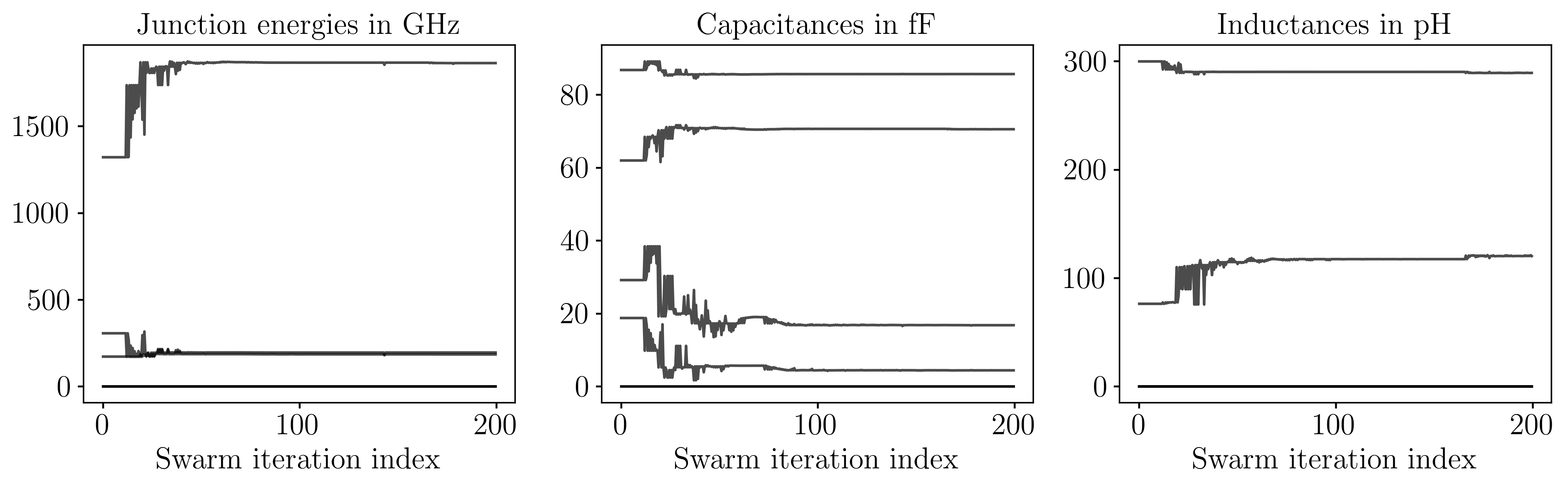
In the discussion of the 4-local coupler search results in Sec. III.2, three circuits are highlighted: circuits C, D, E. Here we provide additional details about the layout, parameters, and spectra of these circuits. The inductive network of the circuits and their spectra before refinement, after refinement, and with flux offset in a non-primary loop are shown in Fig. S.18. The circuit parameters before and after refinement are listed in Table S.1, and the evolution of the parameters throughout the swarm optimization is shown in Fig. S.19 for circuit C. The double-well properties and 4-local coupling strengths (only for refined circuits) are shown in Table S.2. The 4-local coupling strength is determined in a full system simulation of four qubits and the coupler, which is described in more detail in Sec. S.6.
We observe that the swarm optimization step increases the double-well peak and excited state splitting while keeping the asymmetry induced by the non-primary flux offset small. Therefore, the decreasing (more negative) merit value reflects an improvement of the circuit properties as desired. The reduced or absent 4-local coupling in the full system simulation of circuits D and E shows that the isolated circuit properties do not translate one-to-one to the coupled circuits. However, in the case of circuit C, SCILLA was still able to design a coupler with several hundred MHz of 4-local coupling strength using the double-well merit.
| Circuit C | |||||||||
|---|---|---|---|---|---|---|---|---|---|
| Parameter | |||||||||
| Before refine | 98.8 fF | 15.0 fF | 38.7 fF | 67.5 fF | 1865 GHz | 187 GHz | 192 GHz | 293 pH | 98.1 pH |
| After refine | 85.7 fF | 4.46 fF | 16.8 fF | 70.6 fF | 1865 GHz | 196 GHz | 185 GHz | 289 pH | 120 pH |
| Circuit D | |||||||||
| Parameter | |||||||||
| Before refine | 86.7 fF | 5.74 fF | 77.1 fF | 683 GHz | 1005 GHz | 1039 GHz | 189 pH | 158 pH | 188 pH |
| After refine | 81.5 fF | 2.66 fF | 67.0 fF | 544 GHz | 902 GHz | 911 GHz | 158 pH | 170 pH | 166 pH |
| Circuit E | |||||||||
| Parameter | |||||||||
| Before refine | 66.9 fF | 42.6 fF | 68.5 fF | 1950 GHz | 767 GHz | 611 GHz | 92.7 pH | 204 pH | |
| After refine | 60.3 fF | 35.6 fF | 73.8 fF | 1905 GHz | 801 GHz | 640 GHz | 85.7 pH | 188 pH | |
| Circuit instance | ||||
|---|---|---|---|---|
| Circuit C before refine | 1.24 GHz | 0.51 GHz | 0.20 GHz | |
| Circuit C after refine | 1.50 GHz | 0.87 GHz | 0.20 GHz | 0.573 GHz |
| Circuit D before refine | 0.84 GHz | 0.42 GHz | 0.73 GHz | |
| Circuit D after refine | 1.50 GHz | 3.12 GHz | 0.67 GHz | small |
| Circuit E before refine | 0.26 GHz | 9.23 GHz | 0.27 GHz | |
| Circuit E after refine | 0.24 GHz | 10.8 GHz | 0.27 GHz | small |
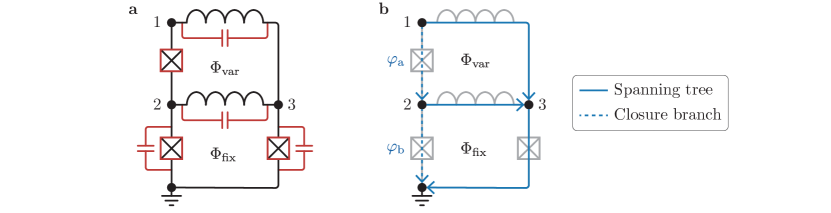
Appendix S.5 Derivation of the circuit C Hamiltonian
In this section, we derive the Hamiltonian of circuit C using the general procedure referenced in Sec. II of the main text. We note that in the automated discovery software, the circuit Hamiltonian is constructed and solved automatically. By re-deriving it here and numerically comparing the spectrum to the result from SCILLA, we show the validity of the automated discovery result and rule out that the software has exploited special cases or bugs in the circuit simulator code that produce unphysical double-well spectra. In fact, one limitation of earlier versions of the code was that promising search results were shown to be unphysical upon closer examination. Additionally, the derivation here demonstrates a practical example of the circuit quantization method.
As described in [S7], the circuit Hamiltonian can be written as the sum of a kinetic (capacitative) term and an inductive potential:
where is the vector of node charges and is the vector of node fluxes. The node capacitance matrix is constructed from the capacitive network of the circuit, which is shown in red in Fig. S.20(a): Diagonal elements are the sum of capacitances connected to a node, and off-diagonal elements are the negative capacitance between two nodes. We determine the capacitance matrix as
where we defined . The pseudo-inverse node inductance matrix is determined by placing the inverses of all linear inductances connected to a node on the diagonal and the negative inverse inductance between two nodes on the off-diagonal:
The set contains the pairs of indices for all nodes that have a junction between them and denotes the phase difference across the junction between nodes and .
In the next step, we impose the boundary conditions of fluxoid quantization. This requires the definition of a spanning tree and closure branches. As all nodes are connected inductively, the spanning tree and closure branch definitions are only necessary for the circuit’s inductive network. We choose their configuration as shown in Fig. S.20(b). The closure branches are chosen across junctions J12 and J22 and we label their respective phase differences as and . Fluxoid quantization yields the following relations:
Here we defined . The inductance matrix has rank 2, so the canonical variables can be transformed to write as a single block. This is achieved with the following transformation matrix:
The variables and matrices are transformed as follows:
The matrix is diagonal with only two non-zero entries, which are the inductances of the oscillator modes of the circuit:
Therefore, we write the transformed nodes and in the oscillator basis and nodes , which is not connected to a linear inductance, in the charge basis. The frequencies and impedances of the oscillator modes are calculated as follows:
where denotes the entries of the rotated inverse capacitance matrix .
We also apply the variable transformation to the flux variables in the Josephson potential terms. The cosines are then written as exponentials, which are recognized as quantum optical displacement operators for the nodes written in the oscilator basis:
In the charge basis, the exponentials transform to charge displacement operators for node :
| (2) |
Thus, all the inductive terms in the circuit Hamiltonian are written in the desired mixed-basis representation of oscillator and charge basis. We are left with the capacitative terms that include off-diagonal elements of . These are of the form . The charge operators of nodes and are written in the oscillator basis, and the charge operator of node is kept and represented in the charge basis.
The circuit Hamiltonian after transformation and expression in the mixed-basis representation separates into terms of the oscillator modes & only, charge mode only, and interactions between the oscillator and charge modes. To structure the lengthy Hamiltonian expression, we separate it into a sum of an oscillator Hamiltonian , charge Hamiltonian , and interaction Hamiltonian :
Here, and are the bosonic raising and lowering operators and “h.c.” is short for the hermitian conjugate of the preceding term. We simulate the spectrum of this Hamiltonian in Python and confirm that it matches the one calculated by the circuit simulator in SCILLA, which is shown in Fig. S.18.
Appendix S.6 Full system simulation of four qubits and coupler
In Sec. III.2, a full system simulation is presented in which four flux qubits are mutually inductively coupled to circuit C. The simulated circuit is shown in Fig. 4(c) and its spectrum for commonly sweeping the external flux of the qubits around degeneracy is shown in Fig. 4(d). The simulation shows that circuit C mediates a 4-local interaction between the qubits and confirms that the double-well merit can be used as a proxy to optimize such a coupling. Here we provide additional details on the parameters and simulation technique for the full system simulation.
The qubits are three-junction flux qubits with a linear loop inductance and a shunt capacitance across the small junction. The small junction has a Josephson energy of and the large junction an energy of . A linear inductance of and shunt capacitance of are chosen. With those parameters, the qubits are close to the C-shunt flux qubit regime [S8]. Their persistent current is and the linear inductance is chosen to allow for sufficient mutual inductive coupling to shift the coupler flux between its bias points along the double-well ground state spectrum.
The full system Hamiltonian is determined via the general method referenced in Sec. II, with the mutual inductive couplings between the subsystems included in the pseudo-inverse inductance matrix . As the size of the Hamiltonian is too large for a Hilbert space truncation that preserves accuracy of the simulation, a hierarchical diagonalization approach is adopted in which the subsystems are diagonalized first. Since the subsystems are weakly coupled relative to the intra-subsystem modes, they can be combined to the full system in a second diagonalization step.
The mutual inductance required to match the flux shifts induced by the qubit excitation manifolds on the coupler with the double-well bias points for 4-local coupling (red dots in Fig. 4(a)) is not known a priori. Therefore, the optimal qubit-coupler mutual inductance is determined in a parameter sweep and found to be . We note that the mutual inductance can be lowered at the expense of raising the qubit persistent current, which would increase the qubits’ flux noise sensitivity. Finally, we point out that the design of the full system requires further investigation. The goal of this work, however, primarily lay in finding a circuit that exhibits the desired spectral properties and holds promise for experimental implementation of a 4-local interaction between qubits.
-
[S1]
J. L. Morales and J. Nocedal, ACM Transactions on Mathematical Software (TOMS) 38, 7 (2011).
-
[S2]
A. S. Lewis and M. L. Overton, Submitted to SIAM Journal on Optimization (2009).
-
[S3]
Y. Shi and R. Eberhart, in International Conference on Evolutionary Computation Proceedings. IEEE World Congress on Computational Intelligence (IEEE, 1998) pp. 69–73.
-
[S4]
R. Eberhart and J. Kennedy, in Proceedings of the Sixth International Symposium on Micro Machine and Human Science (IEEE, 1995) pp. 39–43.
-
[S5]
L. J. V. Miranda et al., Journal of Open Source Software 3, 21 (2018).
-
[S6]
The automated discovery implementation for use with a generic circuit simulator (not provided) is available at the following address: https://github.com/aspuru-guzik-group/scilla.
-
[S7]
A. J. Kerman, Efficient, hierarchical simulation of complex Josephson quantum circuits, in preparation.
-
[S8]
F. Yan, S. Gustavsson, A. Kamal, J. Birenbaum, A. P. Sears, D. Hover, T. J. Gudmundsen, D. Rosenberg, G. Samach, S. Weber, et al., Nature Communications 7, 12964 (2016).