2D-Dirac surface states and bulk gap probed via quantum capacitance in a 3D topological insulator
Abstract
BiSbTeSe2 is a 3D topological insulator (3D-TI) with Dirac type surface states and low bulk carrier density, as donors and acceptors compensate each other. Dominating low temperature surface transport in this material is heralded by Shubnikov-de Haas oscillations and the quantum Hall effect. Here, we experimentally probe and model the electronic density of states (DOS) in thin layers of BiSbTeSe2 by capacitance experiments both without and in quantizing magnetic fields. By probing the lowest Landau levels, we show that a large fraction of the electrons filled via field effect into the system ends up in (localized) bulk states and appears as a background DOS. The surprisingly strong temperature dependence of such background DOS can be traced back to Coulomb interactions. Our results point at the coexistence and intimate coupling of Dirac surface states with a bulk many-body phase (a Coulomb glass) in 3D-TIs.
An ideal three-dimensional (3D) topological insulator (TI) is a band insulator, characterized by a gap in the single-particle energy spectrum, and symmetry protected, conducting surface states Hasan and Kane (2010); Ando (2013) (and references therein). Experimentally available TIs like Bi2Se3 or Bi2Te3 are, however, far from ideal as they feature, due to intrinsic defects, a relatively high electron or hole density larger than 1018 cm-3 (see Borgwardt et al. (2016) and references therein). By combining p-type and n-type TI materials, i.e., by compensation, the bulk concentration can be suppressed Ando (2013); Ren et al. (2011). This comes at the price of large potential fluctuations at low temperatures as the resulting ionized donor and acceptor states are poorly screened and constitute a randomly fluctuating Coulomb potential, bending the band edges and creating electron and hole puddles Skinner et al. (2012, 2013). These were observed by, e.g., optical spectroscopy Borgwardt et al. (2016) and scanning tunneling experimentsKnispel et al. (2017). In the absence of metallic surface states, i.e., in compensated conventional semiconductors, variable range hopping governs low-temperature transport ( 100 K) Efros and Shklovskii (1984); Skinner et al. (2012). Recently, Skinner et al. have shown that the electronic density of states (DOS) in the bulk is nearly constant under these circumstances and features a Coulomb gap at the Fermi level Skinner et al. (2012, 2013). In 3D-TIs, in addition, Dirac surface states, which form a two-dimensional (2D) electron (hole) system, encase the bulk and constitute the dominating transport channel at low temperatures.
The nature of the surface and bulk phases is antithetical. The helical surface metal is an example of Berry Fermi liquid Chen and Son (2017), whose constituents are resilient to Anderson localization Hasan and Kane (2010) and well described within a single (quasi-)particle picture. Bulk electrons on the other hand are topologically trivial, and organize into a many-body disordered and localized phase. Indeed, such a phase shows characteristics Skinner et al. (2013); Meroz et al. (2014) typically ascribed to a Coulomb glass, an exotic insulating state known and studied for decades, yet far from being fully understood Davies et al. (1984); Vignale (1987); Ovadyahu (2013). The interplay between these two different phases is largely unexplored ground, one reason being the difficulty in engineering a system where both coexist. A largely-compensated 3D-TI like BiSbTeSe2 seems however ideally suited for this purpose, appearing as an intrinsic two-phase hybrid system. Moreover, understanding the surface-bulk interplay is not only interesting for fundamental reasons, but also necessary if BiSbTeSe2 – and more generally (fully-)compensated 3D-TIs – is used as a device platform to realize, for example, topological superconductivity, Majorana zero modes Fu and Kane (2008, 2009), and topological magnetoelectric effects Essin et al. (2009). With this goal in mind, we explore the surface-bulk interplay by probing the DOS of the Dirac surface states.
The method we used is capacitance spectroscopy, which provides complementary information, compared with common transport measurements. The total capacitance , measured between a metallic top gate and the Dirac surface states, depends on the geometric capacitance, , and the quantum capacitance ,
| (1) |
Here , are, respectively, relative dielectric constant, and thickness of the insulator, as well as capacitor area, the vacuum dielectric constant, and the DOS at the Fermi level (chemical potential) . The quantum capacitance, connected in series to , reflects the energy spectrum of 2D electron systems Smith et al. (1985); Mosser et al. (1986); Ponomarenko et al. (2010), and probes preferentially the top surface DOS in 3D-TIs Kozlov et al. (2016). At higher temperatures, has to be replaced by the thermodynamic density of states (TDOS) at , , with the carrier density. While gating of 3D-TIs and tuning of the carrier densities of top and bottom surfaces Fatemi et al. (2014); Xiong et al. (2013); Chong et al. (2019), and even magnetocapacitance Chong et al. (2019, 2020) has been explored in the past, the analysis of quantum capacitance and the DOS in a compensated TI like BiSbTeSe2 remained uncharted. Our measurements show that, while Dirac surface states dominate low- transport as expected, the bulk provides a background, capable of absorbing a large amount of charge carriers. These missing charges are very common in 3D-TI transport experiments, yet to the best of our knowledge unexplained Xu et al. (2016); Zhang et al. (2017); Chong et al. (2018); Yoshimi et al. (2015). Furthermore, our in-depth analysis of the quantum capacitance data shows that the background is not a rigid object, but reorganizes itself depending on the gate voltage (and temperature) value. This is a signature of a strongly interacting many-body phase, whose effective single-particle DOS reshapes itself adapting to varying conditions – e.g. when charges are added or removed. The reshaping is typically slow, with a reaction/relaxation time which can be orders of magnitude slower than that of the surface Dirac metal. This provides evidence that BiSbTeSe2 is not an ideal 3D-TI, but rather a hybrid two-phase system, and suggests that similar behavior should be expected for other compensated 3D-TI materials.
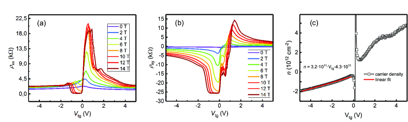
Transport measurements – The details of sample fabrication and measurements can be found in Supporting Information. Fig. 1(a) and 1(b) display the layer sequence and an optical micrograph of one of the devices, respectively. Temperature dependent measurements show (see Fig. S2 in the Supporting Information) that at 1.5 K transport is entirely dominated by the surface with negligible contribution from the bulk. The carrier density and of top and bottom surfaces can be adjusted by top and bottom gate voltages, , respectively. This is shown for the Hall resistivity at 14 T in Fig. 1(c). The device displays well developed quantum Hall plateaus at total filling factor -1, 0 and 1 (Note that for each Dirac surface state, Landau levels are fully filled at half integer and total filling factor 1, corresponding to on top and bottom surfaces Xu et al. (2016).). The plateaus are well separated from each other and marked by dashed purple lines. As these lines run nearly parallel to the - and -axes, respectively, we conclude that the carrier density on top and bottom can be tuned nearly independently.
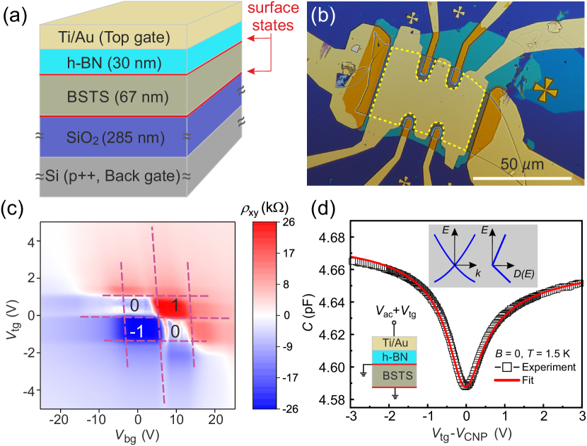
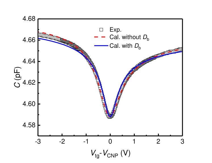
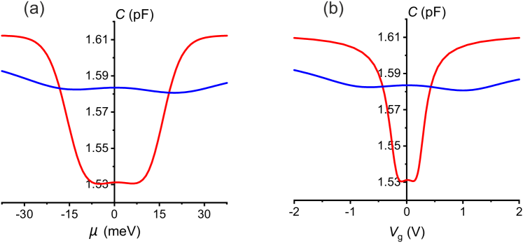
Capacitance measurements – Figure 1(d) shows the measured capacitance , which is directly connected to the DOS, see Eq. (1) (measurement details are in the Supporting Information). The measured trace with a minimum at the Dirac or charge neutrality point (CNP) resembles the quantum capacitance measured for graphene, apart from a pronounced electron-hole asymmetry Ponomarenko et al. (2010); Yu et al. (2013); Xia et al. (2009) due to a parabolic contribution to the linear dispersion Taskin et al. (2011). Explicitly, the latter reads , with the reduced Planck constant, the Fermi velocity at the Dirac point, and the effective mass. It is sketched in the upper inset of Fig. 1(d), together with the electron-hole asymmetric, nearly -linear DOS, given by . Here we used that and .
While in a perfect system vanishes at the CNP, disorder smears the singularity, as in case of graphene Ponomarenko et al. (2010). We model the potential fluctuations by a Gaussian distribution of energies with width , resulting in an average DOS . To convert energies into voltages we use , with the elementary charge and describing at zero voltage. By fitting to the data in Fig. 1(d) we extract meV, m/s and ( free electron mass). The broadening , which is in reasonable agreement with theorySkinner and Shklovskii (2013), is only important in the immediate vicinity of the CNP but hardly affects the values of and . The obtained and values agree well with ARPES data Arakane et al. (2012); Fatemi et al. (2014) and values extracted from Shubnikov-de Haas oscillations Taskin et al. (2011).
-field dependence of capacitance measurements – Our key result arises when we crank up the magnetic field and measure signatures of the Landau level (LL) spectrum, shown in Fig. 2(a). At the 0-th LL level position a local maximum emerges with increasing -field, flanked by minima at each side. The two minima, highlighted by arrows, correspond to the Landau gaps between LLs 0, and (see Fig. 2(a)). Due to the large broadening, higher LLs do not get resolved. Lowering down to 50 mK does not resolve more structure, indicating that disorder broadening is the limiting factor. By sweeping across the 0-th LL, i.e., from arrow position to arrow position, the carrier density changes by the LL degeneracy . In contrast, the change of carrier density , calculated via capacitance, , is by a factor 1.4 higher. Hence, we must assume that a large fraction of the carriers, induced by field effect, ends up in the bulk and is localized at low .
To compare with these experiments we calculate using Gaussian-broadened LLs, , with broadening . The LL spectrum dispersion reads Taskin and Ando (2011)
| (2) |
with , and the tiny Zeeman splitting was neglected. Using the above DOS is insufficient to describe the data - the calculated distance between adjacent Landau gaps is too small and does not match the minima positions observed in experiment (marked by arrows in Fig. 2(a) for the 14 T trace, see Fig. S4 in the Supporting Information as an example). is the voltage needed to fully fill the 0-th LL of the surface states. Since in experiment is larger than that in calculation (relies on the filling rate ), it means that a fraction of the field-induced electrons does not go to the surface states but eventually into the bulk. Thus a higher voltage (higher ) is needed to fill the zeroth LL. In contrast, we obtain almost perfect agreement – see Fig. 2(b) – if we introduce an energy-independent background DOS which models these bulk states. The calculated TDOS we compare with experiment thus reads
| (3) |
with the Fermi function.
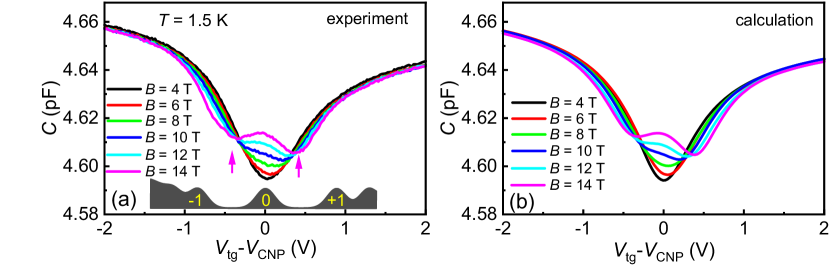
As shown in Fig. 2(b), the constant background leads to excellent agreement with experiment. Although the bulk DOS is hardly directly accessible by the quantum capacitance itself (i.e., by its value), we probe it indirectly via the missing charge carriers given by the Landau gap positions. This missing charge carrier issue holds also for the quantum Hall trace in Fig. 1(c), where 30% of the induced electrons are missing. Indeed, it also appears in several other publications with missing electron fractions ranging from 30% (as here) to 75% (see Xu et al. (2016); Zhang et al. (2017); Chong et al. (2018); Yoshimi et al. (2015)).
The bottom line is: The change of surface carrier density extracted from the Landau gap positions is smaller than the one ”loaded” into the system within the same voltage interval. Further, the filling rate determined by the classical Hall effect at 1.5 K is consistent with the one found for the surface states (see the Supporting Information). Thus, the charge carriers loaded at low into the bulk are localized and do not contribute to transport. This is consistent with transport experiments Xu et al. (2014, 2016), and also in line with what is expected in compensated semiconductors Efros and Shklovskii (1984), as was recently highlighted in Ref. Skinner et al. (2012). There, bulk transport of compensated TI was considered, where local puddles of n- and p-regions form. In this regime, low- transport is governed by variable range hopping, the DOS is, apart from the Coulomb gap, essentially constant for perfect compensations but changes its form strongly if the chemical potential shifts. Efros and Shklovskii (1984); Skinner et al. (2012, 2013)
Using a constant background affects somewhat the values extracted above from . Thus, we fitted the trace in Fig. 1(d) using the same . Now a reduced broadening meV is needed, which is still in reasonable agreement with theorySkinner and Shklovskii (2013). is then best described by slightly modified values: m/s and , respectively, still compatible with results reported elsewhere Arakane et al. (2012); Fatemi et al. (2014); Taskin et al. (2011).
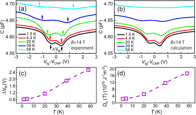
Temperature dependence of quantum capacitance – The background DOS rises quickly with temperature. Corresponding data for 14 T and various s up to 58 K is shown in Fig. 3(a). The local minima due to Landau gaps, marked by arrows, shift with increasing to larger . The corresponding is shown in Fig. 3(c). For fixed the Landau degeneracy is constant and does not depend on temperature. The increasing needed to fill the 0-th LL of the surface states thus indicates that, with increasing , more carriers are lost to the bulk. Similar behavior was found for quantum Hall data Xu et al. (2016, 2014). Clearly, to model the Landau gap positions correctly, a strongly -dependent thermodynamic density of states (TDOS) is required. A simple approach consists in introducing a -dependent background DOS, . Its values used to fit the data of Fig. 3(a) are shown in Fig. 3(d); the resulting traces for different temperatures are plotted in Fig. 3(b). is nearly constant at low but rises quickly at higher temperatures, as shown in Fig. 3(d). However, a closer inspection of the possible microscopic origins of reveals the central issue hiding behind our data: How can the TDOS near the Dirac point (at 14 T the Landau gaps are located between -30 meV and +30 meV, as estimated by Eq. (2)) be at the same time practically flat, yet so strongly -dependent? One could attempt to explain its constant value at 1.5 K by conventional trapped surface states between BSTS and hBN. They are likely responsible for the small hysteresis observed when sweeping , but the - trace shift for up- and down-sweep first stays constant at low , then drops with increasing temperature (see the Supporting Information). This rules out the interface states as reason of the striking TDOS increase with . Alternatively, one could argue that the increased TDOS stems from thermal smearing of the DOS of the (effective) band edges, separated by a reduced gap of meV, as determined by the measured activation energy (see the Supporting Information), instead of the full gap of 300 meV. Modeling this scenario by choosing the DOS at the band edges such that the average TDOS, when sweeping from one Landau gap to the other, equals the extracted constant cannot explain the experimental traces: The resulting TDOS is strongly energy-dependent, reflecting the sharp DOS shoulders at the band edges, and this strong dependence would completely dominate the capacitance signal (Fig. S10 in the Supporting Information). Thus, we are unable to find a single-particle DOS which is consistent with the experimental findings, suggesting that a single-particle picture is simply not adequate.
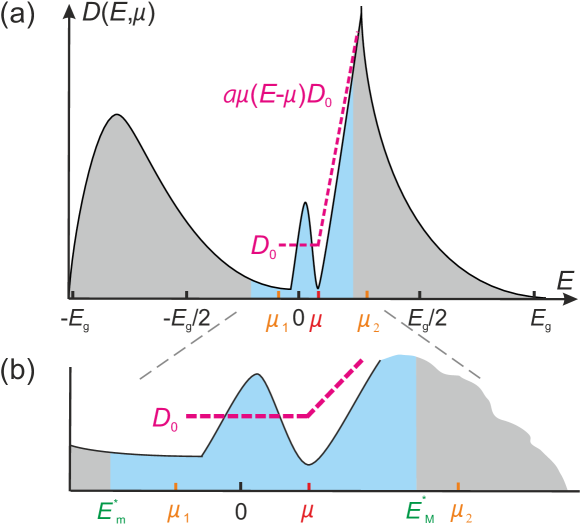
Probing the many-body background – A way out of this apparent dead-end is provided by the strongly fluctuating potential landscape of compensated TIs like BiSbTeSe2, sketched in Fig. 4(a)-(b), where Coulomb interaction dominates Skinner et al. (2012): In a nutshell, the background DOS emerges as an effective single particle DOS describing the ensemble of strongly interacting electrons filling bulk impurity states Efros and Shklovskii (1984). As such, it is actually a - and -dependent object, ,
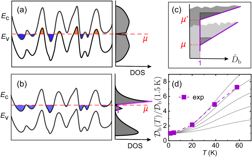
which in particular can massively reshape itself when is varied Skinner et al. (2013), see Fig. 4(a)-(b). The reshaping is a complex many-body problem and can be very slow Amir et al. (2011); Ovadyahu (2013). The situation is further complicated by the presence of the Dirac surface states encasing the bulk. Since precise timescales for BiSbTeSe2 are not known, and a comprehensive theory covering all aspects of our 3D TI scenario is not available, we can only argue along phenomenological lines. First, the timescale of about 1 minute needed to produce each data point after changing is assumed sufficiently long for the reshaping to take place, at least partially. Second, we look for a bare-bone DOS toy model meeting three fundamental constraints: (i) the resulting TDOS is everywhere constant but strongly -dependent; (ii) the overall number of charges lost to the bulk when scanning from one Landau gap to the other increases by a factor of roughly 8 in the interval K to K; (iii) its shape is qualitatively compatible with established theoretical results Skinner et al. (2013). Consider therefore the TDOS
| (4) |
the -derivative acting on both the Fermi function and . The background DOS is given by a toy model: 111We do not consider an explicit -dependence of the DOS as too little precise knowledge is available for a meaningful guess. Note also that we ignore the presence of a Coulomb gap Efros and Shklovskii (1984); Grunewald et al. (1982); Mogilyanskii and Raikh (1989); Sandow et al. (2001); Vaknin et al. (2002); Bardalen et al. (2012); Meroz et al. (2014). This is because the gap is a function of , not of alone, and thus its contribution to can be neglected, at least within our phenomenological approach (see the Supporting Information).
| (5) |
Here is the TDOS value measured at , is a parameter, while are cut-off energies such that , with the position of the lower Landau gap and K (see corresponding sketch in Fig. S11 in the Supporting Information). Beyond such cut-offs the form of is irrelevant for computing the corresponding TDOS. The dimensionless is sketched in Fig. 4(c) for two different values of . Notice that such a DOS is the result of a reorganization of impurity states, not of the appearance of additional states. That is, it is constrained by the condition that the overall number of donors and acceptors states within the gap is fixed. Thus, its profile above sharpens because impurity states from higher energies migrate closer to the chemical potential as the latter increases, while it stays flat below as it represents only the average value of the DOS in the region (see sketch in Fig. 4(c), and Fig. S11 in the Supporting Information). In other words, consider two values of the chemical potential , both within the energy region defined by the position of the lower () and upper Landau gap (): The DOS reorganization is such that more higher energy states are available within of than within of , see hatched areas in Fig. 4(c), and this difference is responsible for a strongly -dependent TDOS (see the Supporting Information). Thus, the overall amount of charges lost to the bulk between and is
| (6) |
As discussed above, this quantity cannot be written as , in terms of a rigid single-particle DOS . In Fig. 4(d) we compare the measured TDOS normalized to its K value, , and the one computed from Eqs. (4) and (5). Qualitatively, the similarity is evident. We emphasize however that our toy model can only be taken as an empirical guide to the data.
Conclusions – By probing the capacitance of a BiSbTeSe2 capacitor structure we are able to extract the electronic DOS as a function of the gate voltage (chemical potential ). Our experimental data, together with the calculations, show that the filling (via field-effect) of Dirac surface states and conventional bulk states is closely intertwined. While we observe the Landau quantization of the Dirac surface states in the quantum capacitance signal, the position of the Landau gaps and their increased separation on the gate voltage scale with increasing temperature can only be understood by considering bulk states. These experiments provide a so far unknown method to investigate the many-particle DOS of the bulk of a highly compensated TI. We find the corresponding bulk TDOS to be constant as a function of , but strongly temperature dependent. This result is incompatible with a single-particle picture, and is evidence of the many-body character of the bulk phase. Indeed, the in-depth analysis of quantum capacitance data suggests that the background density of states reorganizes whenever the gate voltage (chemical potential) is changed, on the time scale of a minute. This is compatible with the slow (glassy) dynamics of a disordered and strongly interacting phase Ovadyahu (2013); Meroz et al. (2014), as expected in the bulk of a compensated TI Skinner et al. (2013); Borgwardt et al. (2016); Knispel et al. (2017). To the best of our knowledge, the dynamics of such a surface-bulk two-phase hybrid system is largely uncharted ground at the moment. However a proper understanding of it is crucial for potential device concepts based on the properties of topological surface states.
Acknowledgements.
We thank F. Evers for inspiring discussions, and G. Vignale for a careful reading of the manuscript. The work at Regensburg was funded by the Deutsche Forschungsgemeinschaft (DFG, German Research Foundation) - Project-ID 314695032 - CRC 1277 (Subprojects A07, A08). This project has received further funding from the European Research Council (ERC) under the European Union’s Horizon 2020 research and innovation programme (grant agreement No 787515, ProMotion), as well as the Alexander von Humboldt Foundation. The work at Cologne was funded by the Deutsche Forschungsgemeinschaft (DFG, German Research Foundation) - Project number 277146847 - CRC 1238 (Subproject A04).References
- Hasan and Kane (2010) M. Z. Hasan and C. L. Kane, “Colloquium: Topological insulators,” Rev. Mod. Phys. 82, 3045–3067 (2010).
- Ando (2013) Yoichi Ando, “Topological insulator materials,” J. Phys. Soc. Jpn. 82, 102001 (2013).
- Borgwardt et al. (2016) N. Borgwardt, J. Lux, I. Vergara, Zhiwei Wang, A. A. Taskin, Kouji Segawa, P. H. M. van Loosdrecht, Yoichi Ando, A. Rosch, and M. Grüninger, “Self-organized charge puddles in a three-dimensional topological material,” Phys. Rev. B 93, 245149 (2016).
- Ren et al. (2011) Zhi Ren, A. A. Taskin, Satoshi Sasaki, Kouji Segawa, and Yoichi Ando, “Optimizing solid solutions to approach the intrinsic topological insulator regime,” Phys. Rev. B 84, 165311 (2011).
- Skinner et al. (2012) B. Skinner, T. Chen, and B. I. Shklovskii, “Why is the bulk resistivity of topological insulators so small?” Phys. Rev. Lett. 109, 176801 (2012).
- Skinner et al. (2013) B. Skinner, T. Chen, and B. I. Shklovskii, “Effects of bulk charged impurities on the bulk and surface transport in three-dimensional topological insulators,” J. Exp. Theor. Phys. 117, 579–592 (2013).
- Knispel et al. (2017) T. Knispel, W. Jolie, N. Borgwardt, J. Lux, Zhiwei Wang, Yoichi Ando, A. Rosch, T. Michely, and M. Grüninger, “Charge puddles in the bulk and on the surface of the topological insulator studied by scanning tunneling microscopy and optical spectroscopy,” Phys. Rev. B 96, 195135 (2017).
- Efros and Shklovskii (1984) A. L. Efros and B. I. Shklovskii, Electronic Properties of Doped Semiconductors (Springer-Verlag, New York, 1984) http://www.tpi.umn.edu/shklovskii.
- Chen and Son (2017) J. Y. Chen and D. T. Son, “Berry fermi liquid theory,” Ann. Phys. (New York) 377, 345 (2017).
- Meroz et al. (2014) Y. Meroz, Y. Oreg, and Y. Imry, “Memory effects in the electron glass,” EPL 105, 37010 (2014).
- Davies et al. (1984) J. H. Davies, P. A. Lee, and T. M. Rice, “Properties of the electron glass,” Phys. Rev. B 29, 4260 (1984).
- Vignale (1987) G. Vignale, “Quantum electron glass,” Phys. Rev. B 36, 8192(R) (1987).
- Ovadyahu (2013) Z. Ovadyahu, “Interacting anderson insulators: The intrinsic electron glass,” C. R. Physique 14, 700 (2013).
- Fu and Kane (2008) Liang Fu and C. L. Kane, “Superconducting proximity effect and majorana fermions at the surface of a topological insulator,” Phys. Rev. Lett. 100, 096407 (2008).
- Fu and Kane (2009) Liang Fu and C. L. Kane, “Josephson current and noise at a superconductor/quantum-spin-hall-insulator/superconductor junction,” Phys. Rev. B 79, 161408(R) (2009).
- Essin et al. (2009) Andrew M. Essin, Joel E. Moore, and David Vanderbilt, “Magnetoelectric polarizability and axion electrodynamics in crystalline insulators,” Phys. Rev. Lett. 102, 146805 (2009).
- Smith et al. (1985) T. P. Smith, B. B. Goldberg, P. J. Stiles, and M. Heiblum, “Direct measurement of the density of states of a two-dimensional electron gas,” Phys. Rev. B 32, 2696–2699 (1985).
- Mosser et al. (1986) V. Mosser, D. Weiss, K.v. Klitzing, K. Ploog, and G. Weimann, “Density of states of gaas-algaas-heterostructures deduced from temperature dependent magnetocapacitance measurements,” Solid State Commun. 58, 5 – 7 (1986).
- Ponomarenko et al. (2010) L. A. Ponomarenko, R. Yang, R. V. Gorbachev, P. Blake, A. S. Mayorov, K. S. Novoselov, M. I. Katsnelson, and A. K. Geim, “Density of states and zero landau level probed through capacitance of graphene,” Phys. Rev. Lett. 105, 136801 (2010).
- Kozlov et al. (2016) D. A. Kozlov, D. Bauer, J. Ziegler, R. Fischer, M. L. Savchenko, Z. D. Kvon, N. N. Mikhailov, S. A. Dvoretsky, and D. Weiss, “Probing quantum capacitance in a 3d topological insulator,” Phys. Rev. Lett. 116, 166802 (2016).
- Fatemi et al. (2014) Valla Fatemi, Benjamin Hunt, Hadar Steinberg, Stephen L. Eltinge, Fahad Mahmood, Nicholas P. Butch, Kenji Watanabe, Takashi Taniguchi, Nuh Gedik, Raymond C. Ashoori, and Pablo Jarillo-Herrero, “Electrostatic coupling between two surfaces of a topological insulator nanodevice,” Phys. Rev. Lett. 113, 206801 (2014).
- Xiong et al. (2013) Jun Xiong, Yuehaw Khoo, Shuang Jia, R. J. Cava, and N. P. Ong, “Tuning the quantum oscillations of surface dirac electrons in the topological insulator bi2te2se by liquid gating,” Phys. Rev. B 88, 035128 (2013).
- Chong et al. (2019) Su Kong Chong, Kyu Bum Han, Taylor D. Sparks, and Vikram V. Deshpande, “Tunable coupling between surface states of a three-dimensional topological insulator in the quantum hall regime,” Phys. Rev. Lett. 123, 036804 (2019).
- Chong et al. (2020) Su Kong Chong, Ryuichi Tsuchikawa, Jared Harmer, Taylor D. Sparks, and Vikram V. Deshpande, “Landau levels of topologically-protected surface states probed by dual-gated quantum capacitance,” ACS Nano 14, 1158–1165 (2020).
- Xu et al. (2016) Yang Xu, Ireneusz Miotkowski, and Yong P. Chen, “Quantum transport of two-species dirac fermions in dual-gated three-dimensional topological insulators,” Nat. Commun. 7, 11434 (2016).
- Zhang et al. (2017) Shuai Zhang, Li Pi, Rui Wang, Geliang Yu, Xing-Chen Pan, Zhongxia Wei, Jinglei Zhang, Chuanying Xi, Zhanbin Bai, Fucong Fei, Mingyu Wang, Jian Liao, Yongqing Li, Xuefeng Wang, Fengqi Song, Yuheng Zhang, Baigeng Wang, Dingyu Xing, and Guanghou Wang, “Anomalous quantization trajectory and parity anomaly in co cluster decorated bisbtese2 nanodevices,” Nat. Commun. 8, 977 (2017).
- Chong et al. (2018) Su Kong Chong, Kyu Bum Han, Akira Nagaoka, Ryuichi Tsuchikawa, Renlong Liu, Haoliang Liu, Zeev Valy Vardeny, Dmytro A. Pesin, Changgu Lee, Taylor D. Sparks, and Vikram V. Deshpande, “Topological insulator-based van der waals heterostructures for effective control of massless and massive dirac fermions,” Nano Lett. 18, 8047–8053 (2018).
- Yoshimi et al. (2015) R. Yoshimi, A. Tsukazaki, Y. Kozuka, J. Falson, K. S. Takahashi, J. G. Checkelsky, N. Nagaosa, M. Kawasaki, and Y. Tokura, “Quantum hall effect on top and bottom surface states of topological insulator (bi1-xsbx)2te3 films,” Nat. Commun. 6, 6627 (2015).
- Yu et al. (2013) G. L. Yu, R. Jalil, Branson Belle, Alexander S. Mayorov, Peter Blake, Frederick Schedin, Sergey V. Morozov, Leonid A. Ponomarenko, F. Chiappini, S. Wiedmann, Uli Zeitler, Mikhail I. Katsnelson, A. K. Geim, Kostya S. Novoselov, and Daniel C. Elias, “Interaction phenomena in graphene seen through quantum capacitance,” Proc. Natl. Acad. Sci. 110, 3282–3286 (2013).
- Xia et al. (2009) Jilin Xia, Fang Chen, Jinghong Li, and Nongjian Tao, “Measurement of the quantum capacitance of graphene,” Nat. Nanotechnol. 4, 505 (2009).
- Taskin et al. (2011) A. A. Taskin, Zhi Ren, Satoshi Sasaki, Kouji Segawa, and Yoichi Ando, “Observation of dirac holes and electrons in a topological insulator,” Phys. Rev. Lett. 107, 016801 (2011).
- Skinner and Shklovskii (2013) Brian Skinner and B. I. Shklovskii, “Theory of the random potential and conductivity at the surface of a topological insulator,” Phys. Rev. B 87, 075454 (2013).
- Arakane et al. (2012) T. Arakane, T. Sato, S. Souma, K. Kosaka, K. Nakayama, M. Komatsu, T. Takahashi, Zhi Ren, Kouji Segawa, and Yoichi Ando, “Tunable dirac cone in the topological insulator bi2-xsbxte3-ysey,” Nat. Commun. 3, 636 (2012).
- Taskin and Ando (2011) A. A. Taskin and Yoichi Ando, “Berry phase of nonideal dirac fermions in topological insulators,” Phys. Rev. B 84, 035301 (2011).
- Xu et al. (2014) Yang Xu, Ireneusz Miotkowski, Chang Liu, Jifa Tian, Hyoungdo Nam, Nasser Alidoust, Jiuning Hu, Chih-Kang Shih, M. Zahid Hasan, and Yong P. Chen, “Observation of topological surface state quantum hall effect in an intrinsic three-dimensional topological insulator,” Nat. Phys. 10, 956 (2014).
- Amir et al. (2011) A. Amir, Y. Oreg, and Y. Imry, “Electron glass dynamics,” Annu. Rev. Condens. Matter Phys. 2, 235 (2011).
- Note (1) We do not consider an explicit -dependence of the DOS as too little precise knowledge is available for a meaningful guess. Note also that we ignore the presence of a Coulomb gap Efros and Shklovskii (1984); Grunewald et al. (1982); Mogilyanskii and Raikh (1989); Sandow et al. (2001); Vaknin et al. (2002); Bardalen et al. (2012); Meroz et al. (2014). This is because the gap is a function of , not of alone, and thus its contribution to can be neglected, at least within our phenomenological approach (see the Supporting Information).
- Grunewald et al. (1982) M. Grunewald, B. Pohlmann, L. Schweitzer, and D. Wurtz, “Mean field approach to the electron glass,” J. Phys. C: Solid State Phys. 15, L1153 (1982).
- Mogilyanskii and Raikh (1989) A. A. Mogilyanskii and M. Raikh, “Self-consistent description of coulomb gap at finite temperatures,” J. Exp. Theor. Phys. 68, 1081 (1989).
- Sandow et al. (2001) B. Sandow, K. Gloos, R. Rentzsch, A. N. Ionov, and W. Schirmacher, “Electronic correlation effects and the coulomb gap at finite temperature,” Phys. Rev. Lett. 86, 1845–1848 (2001).
- Vaknin et al. (2002) A. Vaknin, Z. Ovadyahu, and M. Pollak, “Nonequilibrium field effect and memory in the electron glass,” Phys. Rev. B 65, 134208 (2002).
- Bardalen et al. (2012) E. Bardalen, J. Bergli, and Y. M. Galperin, “Coulomb glasses: A comparison between mean field and monte carlo results,” Phys. Rev. B 85, 155206 (2012).
Supplementary information: 2D-Dirac surface states and bulk gap probed via quantum capacitance in a 3D topological insulator
Jimin Wang,1 Cosimo Gorini,2 Klaus Richter,2 Zhiwei Wang,3,4 Yoichi Ando,3 and Dieter Weiss1
1Institute of Experimental and Applied Physics, University of Regensburg, 93040 Regensburg, Germany
2Institute of Theoretical Physics, University of Regensburg, 93040 Regensburg, Germany
3Physics Institute II, University of Cologne, Zülpicher Str. 77, 50937 Köln, Germany
4Key Laboratory of Advanced Optoelectronic Quantum Architecture and Measurement, Ministry of Education, School of Physics, Beijing Institute of Technology, Beijing, 100081, China
I Details of sample fabrication, transport and capacitance measurements
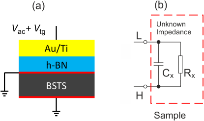
Pristine, slightly -doped BiSbTeSe2 crystals grown by the modified Bridgman method Ren et al. (2011) were used. Angle-resolved photoemission spectroscopy has shown that Dirac point and of this material lie in the bulk gap Arakane et al. (2012). BiSbTeSe2 flakes were exfoliated onto highly -doped Si chips (used as backgate) coated by 285 nm SiO2. The flakes were processed into quasi-Hallbars with Ti/Au (10/100 nm) Ohmic contacts. A larger h-BN flake, transferred on top of BiSbTeSe2 serves as gate dielectric. Finally, Ti/Au (10/100 nm) was used as a top gate contact. Transport measurements using low ac excitation currents (10 nA at 13 Hz) were carried out above 1.5 K and in a cryostat (Oxford instrument) with out of plane magnetic fields up to 14 T.
The capacitance is measured in a straightforward and simple manner using an Andeen Hagerling 2700A capacitance bridge. As we want to measure the capacitance between the gate and the TI layer (Fig. S1a), the gate is connected to the low contact (L) of the bridge and the TI layer is connected to the high contact (H). We were working in the bridge mode where for every data point (capacitance and loss) the bridge is balanced against the device under test (Fig. S1b). The bridge is operating in the frequency range between 50 Hz and 20 kHz; we are using the lowest frequency in order to avoid resistive effects.Kozlov et al. (2016) )
II Resistivity-temperature relation
Fig. S2 shows the temperature dependence of the device discussed in the main part of the text. With decreasing temperature, the resistivity of the device increases down to K, characteristic for semiconductor-like, bulk dominated conduction, and decreases below K, typical for metallic-like, surface dominated conduction.
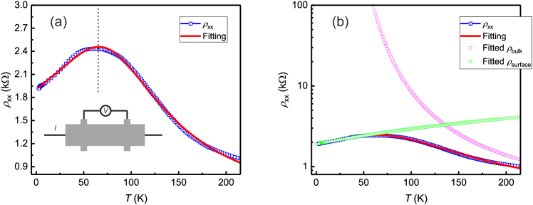
Useful information, such as carrier density and activation energy can be extracted from the graph. Following a recent paper Cai et al. (2018), the surface and the bulk of the topological insulator contribute to the conduction independently, equivalent to resistors connected in parallel. The resistivity of each surface () can be modeled as metallic like, , where and are constants. The bulk resistivity is thermally activated for temperatures beyond the variable range hopping regime: , where is a constant, is half the energy gap , and is the Boltzmann constant. Thus the total resistivity is . Here we assume, for simplicity, that the two surfaces are equivalent, having the same carrier density and mobility . The corresponding fit is shown in Fig. S2a, where we obtained remarkable good agreement. In addition, the fitting also yields , and and thus the effective energy gap . Compared to the nominal energy gap Arakane et al. (2012), the effective gap is 5-times smaller. This is consistent with previous reportsSkinner et al. (2012) and due to thermal excitation of electrons from the Fermi-level to the percolation energy which is much closer to than the band edge.
At sufficiently low temperature (, K), the conduction is almost entirely dominated by Dirac surface states, also verified in Ref. Xu et al. (2014). However, at higher temperatures, bulk carriers are activated and contribute to transport. At = 58 K, using the results from the fit above, and by assuming a typical, temperature independent value of cm2/Vs, we obtain cm-2. The same way, the carrier density at zero gate voltage on each surface is cm-2, using cm2/Vs. Thus the delocalized bulk carrier density at high is comparable to that in the surface states.
III Determining
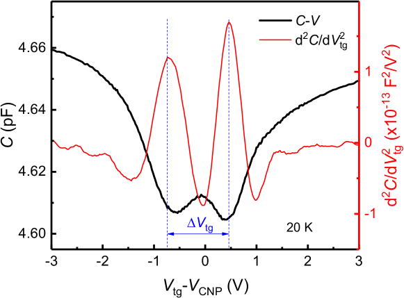
Here we show how in Fig. 2 and Fig. 3 is determined. As an example we use the experimental data taken at 20 K and 14 T, shown in Fig. S3. To enhance the visibility of the minima and to suppress effects of the background we calculate the second derivative of the trace. This results in two pronounced peaks at the position of the minima. The distance between the 2 peaks gives . This procedure is particularly useful at elevated temperatures where it is more difficult to determine the minimum position accurately from the original capacitance trace.
IV Failure of fitting C-V trace at 14 T without background DOS
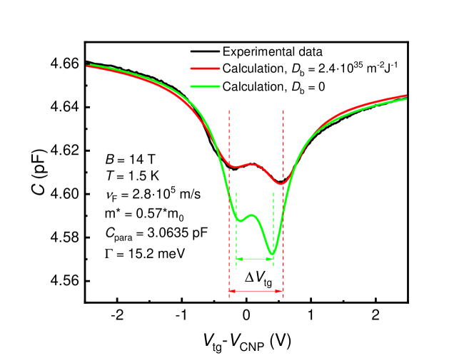
In Fig. S4 we compare the capacitance measured at T and K to fits with and without using a constant background density. The fits without background density fail to describe the data, especially the voltage difference between the capacitance minima which correspond to the Landau gaps. The distance between calculated, adjacent Landau gaps is always smaller (marked by in Fig. S4) than observed in experiment if is set to 0, no matter how the other parameters are chosen. This discrepancy becomes much larger at higher temperatures.
V Transport data and estimating the filling rate from Hall measurements
Fig. S5a and Fig. S5b show and vs at = 0 V and different . Note, that in transport top and bottom surfaces contribute to the signal while in capacitance experiments we probe preferentially the top surface. Therefore, capacitance and transport data cannot directly be compared. The data shown here are consistent with Fig. 1c in the main text.
The filling rate extracted from the position of the Landau gaps on the gate voltage scale in the main text (Fig. 2(a) and Fig. 3(a)) is smaller than , expected from the insulator capacitance , is the area of the capacitor. Fig. S5c shows that the reduced filling rate is also measured by the classical Hall slope.
The Hall data were taken at 1.5 K by sweeping the top gate voltage () at fixed , as well as by sweeping at fixed , at = 0 V. The device shows at such low temperature surface dominated conduction, which takes place in top and bottom surface. From Fig. 1(c) in the main text, we see that at zero gate voltage, both top and bottom surfaces are slightly p-doped. By grounding the back gate and sweeping from 5 to -5 V, one changes the carrier type in the top surface. For in Fig. S5c, p-type conduction prevails in top and bottom surfaces. The total carrier density and the total filling rate in this regime can be simply obtained from the one carrier Drude model using the linear Hall slope. The filling rate, i.e., the change of total density with gate voltage, is given by the slope of the red line in Fig. S5c. The corresponding filling rate is . This is consistent with the filling rate displayed by the QHE data in the main text (, using V from Fig. 3(c)). Similar conclusions can be found in Xu et al. (2014).
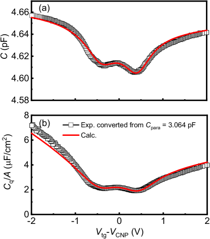
VI Comparing fitting of C-V at T and K with and without background DOS
The capacitance trace in Fig. 1(d) of the main text we fitted without using a background DOS . While the data can be well fitted using , the capacitance data in quantizing magnetic field cannot. In Fig. S6 we show that the data of Fig. 1(d) can be likewise fitted with a finite DOS . As a result, the energy broadening becomes significantly smaller, but the important parameters like Fermi velocity and effective mass stay within 20% the same.
VII Extracting the quantum capacitance from curves
Using Eq.(1) from the main text one can extract the quantum capacitance , which is given by . Here, stands for , used in the main text, and , is the area of the capacitor. The extracted quantum capacitance depends strongly on the parasitic capacitance which needs to be subtracted from the measured to get the real capacitance . is the geometric capacitance given by , where and are dielectric constant and thickness of the gate insulator, respectively. Subtracting and extracting is thus prone to error. This is illustrated in Fig. S7, where we show the extracted quantum capacitance per unit area () using three slightly different (by 0.13%) , both as function of gate voltage and chemical potential.
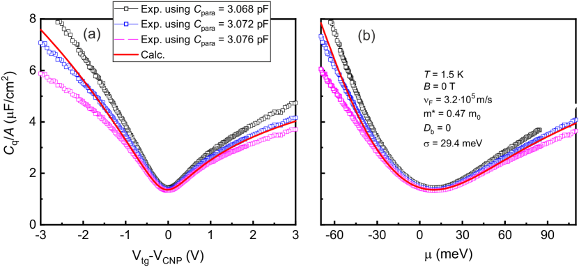
Changing a bit changes the subtracted significantly. It is therefore much less critical to directly fit the capacitance , instead of extracting first the quantum capacitance and then fit . Due to the inaccurately known this is - as pointed out above - prone to error and we cannot expect a reliable fit. In case we fit directly, as we have done, is only a constant offset which shifts the capacitance value on the -axis. After the capacitance has been fitted and determined, the extracted quantum capacitance is equivalent to the one used to fit the capacitance (red solid curves in Fig. S7).
VIII Does the strong temperature dependence of the TDOS come from a single particle gap?
Here we explore the possibility whether the temperature dependent TDOS might stem from a narrowed energy gap, which corresponds to the measured reduced activation energy of about 60 meV (see ”1. Resistivity-temperature relation”). For testing purposes one can ad hoc construct a model DOS which mimics a reduced bandgap (here 60 meV) and adjust the value of the DOS such, that the average TDOS between the two Landau gaps (-20 to 25 meV) corresponds, at high temperatures, to the one observed in experiment (our Fig. 3d). This average TDOS would cause the same shift of the capacitance minima on the gate voltage scale as observed in experiment. This is illustrated by Fig. S9.
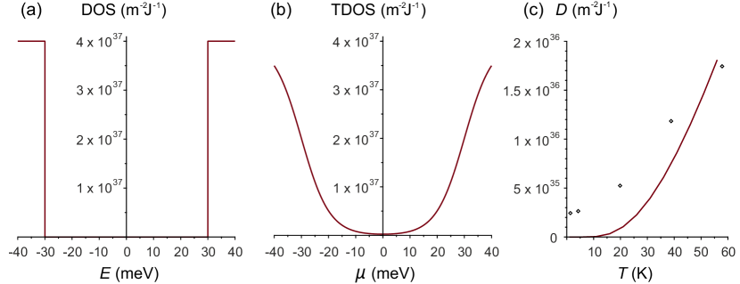
Fig. S9 above shows (a) the corresponding DOS, (b) the TDOS and (c) the average TDOS, intended to mimic our background DOS. However, such a picture is not able to explain the finite DOS (TDOS) we find at the lowest temperatures ( K). Even worse, the strong dependence of the TDOS on is inconsistent with experiment. This is shown in Fig. S10, where we compare, as an example, the 39 K capacitance curve, calculated with a constant background DOS (as the one shown in Fig. 3b of our main text) with the capacitance we obtain from the 39 K TDOS of Fig. S10b.
The strong dependence of the TDOS on completely dominates the capacitance signal so that the additional Landau structure is hardly visible. The shape of the trace is inconsistent with the experimental one. This picture does not change when we vary the parameters, increasing e.g. the “bandgap” and DOS step to keep the average TDOS constant. The density of states we observe in experiment is either nearly constant or has a weak dependence on and thus for the most part cannot come from states energetically far away from .
IX Details on the DOS toy model
We look for a minimal model for the effective DOS qualitatively reproducing the TDOS data, and compatible with known theory results coming from microscopic simulations Skinner et al. (2013). To ease comparison with the latter we consider to be in the -regime, but the construction would be analogous in the -regime. Our model is not -dependent, as too little is known about it with precision for a meaningful guess: On one hand, one expects from general arguments higher temperature to improve screening and thus reduce bulk potential fluctuations Borgwardt et al. (2016); On the other Dirac surface states provide some screening already at Knispel et al. (2017). Our toy model implicitly assumes that -induced screening is negligible compared to that from surface states and from charges added/removed by changing .
We start by splitting the TDOS so as to isolate its -dependent part
| (7) | |||||
where is the Fermi function. One has
| (8) |
Whatever its form, the DOS has to respect the constraint
| (9) |
with respectively the donor and acceptor concentrations in the compensated TI. However we are only concerned with TDOS measurements in the small energy window meV corresponding to the energy difference between the lowest two LL gaps, see Fig. 2 in the main text. We thus need not worry about the DOS normalization condition, and assume the DOS to be of the following (dimensionless) form
| (10) |
Here is a constant with dimensions , and (K) are energy cut-offs, with the position of the lower Landau gap(see sketch in Fig S11). Physically, at the DOS shows features beyond the abrupt increase close to – which is our only concern here. Recall, however, that such an increase requires the DOS to decrease somewhere else, ensuring the overall normalization condition Eq. (9), see Ref. Skinner et al. (2013). Similarly, our data shows that the (average of the) DOS below stays constant – this means, inter alia, that we cannot discern signatures of negative compressibility Eisenstein et al. (1992); Efros (2008) down to K. Its eventual increase at energies is irrelevant for computing away from such a region, see Fig. S11 and corresponding caption. The critical feature of Eq. (10) is that its particle-hole asymmetry, determined by its increase for , depends directly on . This mimics the DOS reshaping, see Fig. S11, and means that at a given more charges can be loaded into the bulk at than at a lower (electro-)chemical potential value , yielding .
In order to see this, consider a variation . From Eq. (10) one obtains the dimensionless TDOS
| (11) | |||||
The integrand is only a function of , ergo the change of variable leads to
| (12) |
which yields
| (13) |
We thus obtain
| (14) |
Note that such a result does not qualitatively change if one generalizes Eq. (10) to
| (15) |
where is a function symmetric around and such that for , which represents the Coulomb gap Efros and Shklovskii (1984); Mogilyanskii and Raikh (1989). Using Eq. (15) would only change the value of the integral , at the price of requiring further assumptions and introducing additional parameters. While a quantitative theory would clearly require taking the Coulomb gap into account, the simpler toy model defined by Eq. (10) is already enough for our discussion and we limit ourselves to it.
X Discussion on frequency dependence
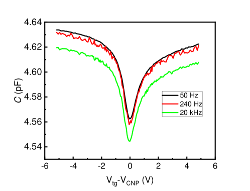
One needs to measure at low frequencies in order to avoid resistive effects, meaning that the measured signal no longer reflects the pure capacitive signal and thus the (thermodynamic) density of states. As emphasized in the main text, we measured at the lowest frequency of 50 Hz in order to avoid such resistive effectsKozlov et al. (2016). Fig. S12 shows -data at 50 Hz, 240 Hz and 20 kHz. The overall dependence on frequency is weak. At the highest frequency of 20 kHz our capacitance bridge allows, the -trace is shifted a bit down but the shape is preserved. This means that the higher frequency has the same effect as a slightly reduced parasitic capacitance. Overall, resistive effects are not very pronounced in this material system. They are e.g., much weaker than at the charge neutrality point in the 3D-topological insulator HgTeKozlov et al. (2016).
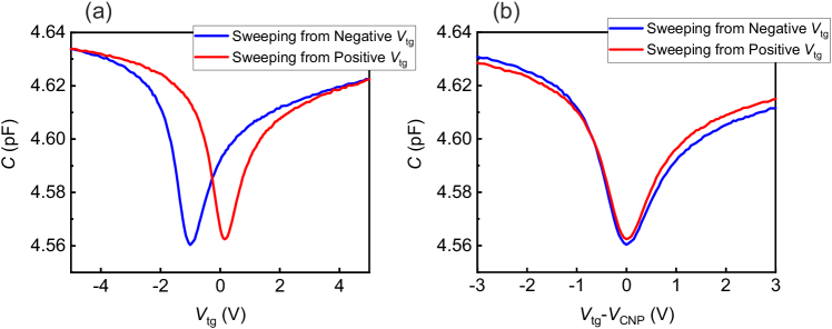
XI Discussion on hysteresis
As mentioned in our main text we take sweeps in one direction only to avoid that hysteresis affects the measurements. Fig. S13a displays up-and down sweep of a trace with clear hysteretic behavior, which we ascribe to charges in the insulator or at the insulator/BSTS interface. The traces are shifted back and forth depending on the sweep direction. In our paper we shift the voltage scale with the origin at the charge neutrality point (CNP). In Fig. S13b we show, by shifting up- and down-sweeps such that they coincide, that the traces are nearly on top of each other. Especially at small voltages between -0.5 and +0.5 V at which the Landau gaps occur, the traces agree well, thus justifying our approach to plot the data on a scale. Hence, the hysteresis does not affect our analysis in the main text. Upon increasing , the hysteresis stays nearly constant before it decreases at elevated and reaches at 90 K about 40% of its low temperature voltage shift. This we checked in another, similar device. We note that the measurements in (Bi1-xSbx)2Te3 (BST) Wang et al. (2019) are carried out in a very different regime. In the BST material investigated there, the Fermi-level is in the conduction band while in the present work it is in the bulk gap of BSTS. In BST the situation is similar to -doped Si where the capacitance value depends on whether the system is under accumulation or inversion. The shape of the traces are looking completely different compared to the one investigated here. In BSTS we have, in contrast to BST, transport which is dominated by the surface states at low temperatures. The traces look thus similar to the ones explored in graphene (apart from the asymmetry with respect to the CNP) or in HgTe Kozlov et al. (2016).
References
- Ren et al. (2011) Zhi Ren, A. A. Taskin, Satoshi Sasaki, Kouji Segawa, and Yoichi Ando, “Optimizing solid solutions to approach the intrinsic topological insulator regime,” Phys. Rev. B 84, 165311 (2011).
- Arakane et al. (2012) T. Arakane, T. Sato, S. Souma, K. Kosaka, K. Nakayama, M. Komatsu, T. Takahashi, Zhi Ren, Kouji Segawa, and Yoichi Ando, “Tunable dirac cone in the topological insulator bi2-xsbxte3-ysey,” Nat. Commun. 3, 636 (2012).
- Kozlov et al. (2016) D. A. Kozlov, D. Bauer, J. Ziegler, R. Fischer, M. L. Savchenko, Z. D. Kvon, N. N. Mikhailov, S. A. Dvoretsky, and D. Weiss, “Probing quantum capacitance in a 3d topological insulator,” Phys. Rev. Lett. 116, 166802 (2016).
- Cai et al. (2018) Shu Cai, Jing Guo, Vladimir A. Sidorov, Yazhou Zhou, Honghong Wang, Gongchang Lin, Xiaodong Li, Yanchuan Li, Ke Yang, Aiguo Li, Qi Wu, Jiangping Hu, Satya K. Kushwaha, Robert J. Cava, and Liling Sun, “Independence of topological surface state and bulk conductance in three-dimensional topological insulators,” npj Quant. Mater. 3, 62 (2018).
- Skinner et al. (2012) Brian Skinner, Tianran Chen, and B. I. Shklovskii, “Why is the bulk resistivity of topological insulators so small?” Phys. Rev. Lett. 109, 176801 (2012).
- Xu et al. (2014) Yang Xu, Ireneusz Miotkowski, Chang Liu, Jifa Tian, Hyoungdo Nam, Nasser Alidoust, Jiuning Hu, Chih-Kang Shih, M. Zahid Hasan, and Yong P. Chen, “Observation of topological surface state quantum hall effect in an intrinsic three-dimensional topological insulator,” Nat. Phys. 10, 956 (2014).
- Skinner et al. (2013) B. Skinner, T. Chen, and B. I. Shklovskii, “Effects of bulk charged impurities on the bulk and surface transport in three-dimensional topological insulators,” Journal of Experimental and Theoretical Physics 117, 579–592 (2013).
- Borgwardt et al. (2016) N. Borgwardt, J. Lux, I. Vergara, Zhiwei Wang, A. A. Taskin, Kouji Segawa, P. H. M. van Loosdrecht, Yoichi Ando, A. Rosch, and M. Grüninger, “Self-organized charge puddles in a three-dimensional topological material,” Phys. Rev. B 93, 245149 (2016).
- Knispel et al. (2017) T. Knispel, W. Jolie, N. Borgwardt, J. Lux, Zhiwei Wang, Yoichi Ando, A. Rosch, T. Michely, and M. Grüninger, “Charge puddles in the bulk and on the surface of the topological insulator studied by scanning tunneling microscopy and optical spectroscopy,” Phys. Rev. B 96, 195135 (2017).
- Eisenstein et al. (1992) J. P. Eisenstein, L. N. Pfeiffer, and K. W. West, “Coulomb barrier to tunneling between parallel two-dimensional electron systems,” Phys. Rev. Lett. 69, 3804 (1992).
- Efros (2008) A. L. Efros, “Negative density of states: Screening, einstein relation, and negative diffusion,” Phys. Rev. B 78, 155130 (2008).
- Efros and Shklovskii (1984) A. L. Efros and B. I. Shklovskii, Electronic Properties of Doped Semiconductors (Springer-Verlag, New York, 1984) http://www.tpi.umn.edu/shklovskii.
- Mogilyanskii and Raikh (1989) A. A. Mogilyanskii and M. Raikh, “Self-consistent description of coulomb gap at finite temperatures,” J. Exp. Theor. Phys. 68, 1081 (1989).
- Wang et al. (2019) Jimin Wang, Markus Schitko, Gregor Mussler, Detlev Grützmacher, and Dieter Weiss, “Capacitance–voltage measurements of (bi1–xsbx)2te3 field effect devices,” physica status solidi (b) 256, 1800624 (2019).