Emergence of a metallic meta-stable phase induced by electrical current in Ca2RuO4
Abstract
A comprehensive study of the behavior of the Mott insulator Ca2RuO4 under electrical current drive is performed by combining two experimental probes: the macroscopic electrical transport and the microscopic X-Ray diffraction. The resistivity, , vs electric current density, , and temperature, , (J,T), resistivity map is drawn. In particular, the meta-stable state, induced between the insulating and the metallic thermodynamic states by current biasing Ca2RuO4 single crystals, is investigated. Such an analysis, combined with the study of the resulting RuO6 octahedra energy levels, reveals that a metallic crystal phase emerges in the meta-stable regime. The peculiar properties of such a phase, coexisting with the well-established orthorhombic insulating and tetragonal metallic phases, allow to explain some of the unconventional and puzzling behaviors observed in the experiments, as a negative differential resistivity.
I Introduction
Ca2RuO4 (hereafter Ca-214) is a paramagnetic Mott insulator subject of extensive experimental and theoretical studies (Gorelov et al., 2010; Sow et al., 2017; Riccò et al., 2018; Das et al., 2018; Porter et al., 2018). The richness of its phase diagram (Steffens et al., 2005; Sow et al., 2017) and the strong interplay between electronic, structural, magnetic and orbital degrees of freedom make the full comprehension of the physics of this system challenging (Mizokawa et al., 2001; Gorelov et al., 2010; Sutter et al., 2017; Das et al., 2018). This material indeed exhibits very different responses, both in the magnetic and transport properties, to different combination of temperature (Nakatsuji and Maeno, 2001; Cao et al., 1997), pressure (Steffens et al., 2005; Nakamura, 2007; Alireza et al., 2010), doping (Carlo et al., 2012; Riccò et al., 2018; Sutter et al., 2019), and electrical field (Nakamura et al., 2013).
Ca-214 is a layered perovskite oxide with Pbca space-group symmetry whose crystallographic unit cell contains four formula units [see Fig. 1(a)]. The fundamental structural units are RuO6 octahedra arranged in corner-shared planes alternated by layers containing the Ca atoms. With respect to the ideal tetragonal structure (with lattice parameters , ), the octahedra bear alternating rotations (about the apical Ru-O2 bond; hereafter), tilts (of with respect to the -plane initially containing the Ru-O1 bonds; and hereafter) and distortions (making and slightly different) (Braden et al., 1998) (see Appendix). The ratios between and and, in particular, between their average, , and determine the relative energies of the orbitals of Ru (, , ), which are the electrons responsible of transport as well as all other response properties. rules the relative position of and levels while rules the relative position of with respect to the - doublet (see Appendix).
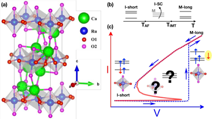
As schematically shown in Fig. 1(b), these ratios change with the temperature, . In particular, increases with , as does ( is the average between and ). For temperatures below the ratio is lower than . As a consequence, the system is an antiferromagnetic (AFM) insulator (Nakatsuji and Maeno, 2001) with lower than - doublet and the four electrons per Ru atom arranged as shown in Fig. 1(c) (I-short). At intermediate and ambient , goes through about , which results in a paramagnetic Strongly Correlated Mott insulator (I-SC) with the three levels almost degenerate (M), before both and go through a Mott-Hubbard splitting (Gorelov et al., 2010; Zhang and Pavarini, 2017). Finally, when is sufficiently larger than , above , the system undergoes an Insulator-Metal transition (IMT) (Nakatsuji and Maeno, 2001) with the four electrons per Ru arranged as shown in the M-long configuration reported in Fig. 1(c). IMT is accompanied by a crystallographic transition from a tetragonal (L-Pbca, L stands for long c) to an orthorhombic (S-Pbca, S short c) phase, so dramatic to break the crystals into pieces (Nakamura et al., 2013).
The strong link between conduction and structural properties (Gorelov et al., 2010; Zhang and Pavarini, 2017) paves the way to control the electronic behavior by strain/epitaxial growth (Kikuzuki and Lippmaa, 2010) or by inducing nonlinear phononic effects, for instance through intense terahertz radiation (Rini et al., 2007; Ehrke et al., 2011; Ichikawa et al., 2011). Another relevant drive to induce the IMT is the electric field, despite the structural changes indirectly induced in such a case are not yet clarified. Indeed, the electric field tuning of the conduction regime is of particular interest, since at room the metallic state can be induced by a threshold field of about (Nakamura et al., 2013; Okazaki et al., 2013; Sow et al., 2017), almost three orders of magnitude lower than in other Mott insulators (Janod et al., 2015). This circumstance is very promising for possible applications in next-generation oxide electronics. As in other Mott materials (Imada et al., 1998; Janod et al., 2015), the IMT is accompanied by resistivity changes of several orders of magnitude (Nakamura et al., 2013). As a first order transition, IMT is generally unveiled by hysteretic electrical transport (Limelette et al., 2003; Nakamura et al., 2013) for voltage drive [Fig. 1(b), blue dotted line]. Instead, voltage-current characteristics with negative slope were reported for dc current drive Fig. 1(c), red line (Okazaki et al., 2013; Zhang et al., 2019).
However, one should be aware that different measurement protocols exist in the literature under the simple names of voltage or current drive. The difference in the procedures on one hand gives new perspective to look at an interesting system such Ca-214, but makes also difficult to compare the results obtained in different works. Recently, the investigation of non-equilibrium electronic and crystallographic phases emerging by current or voltage biasing the crystals gained much attention. Indeed, a new crystal structure supposing to be the manifestation of a new semi-metallic state was reported by a measurement protocol completely different from the one presented in this work (Bertinshaw et al., 2019), while alternating insulating and metallic regions arranged in stripes patterns at the M-I phase boundary were observed in the regime of controlled constant current flow (Zhang et al., 2019). Moreover, it is now accepted that dc current biasing can be used to control the magnetic properties of the system, since, under current flow, strong diamagnetism is induced in pure Ca-214 and in Ca3Ru1-xTixO7 (Sow et al., 2017, 2019) and AFM order is suppressed in pure Ca-214 (Bertinshaw et al., 2019; Sow et al., 2019).
In this work, the electrical response of Ca-214 single crystals is investigated as a function of both and the bias-current density, , in the conduction regimes spanning from the insulating to the meta-stable (MS) state, precursor of the metallic one, where non-equilibrium processes possibly take place. In this way, the resistivity map, , of the system, where is the electrical resistivity, is built. This study, systematically performed on a large number of crystals, is an extremely valuable starting point for further investigations, since it naturally highlights the different conducting regimes, as well as the characteristic temperatures and current densities, at which they set in. In particular, here the attention focuses on the less explored MS state, since poor information are currently available concerning both the conduction mechanisms and the corresponding crystallographic structure. For these reasons, the transport measurements are combined with X-Ray Diffraction (XRD) spectra acquired as a function of , at room .
II Experimental Methods
High quality Ca-214 single crystals were grown by floating zone technique as described in Ref. (Fukazawa et al., 2000). The typical average dimensions of the analyzed crystals are about . Great care was paid to the reproducibility of the presented results. At this purpose a big amount of data was collected on several Ca-214 single crystals, which all behaved consistently. This assures the reliability of the presented measurements.
The phase diagram of Ca-214 is very rich as well as quite far from being fully explored and understood. For this reason, an extremely precise control of the actual state of the sample, as a function of the external conditions, is required in order efficiently study this system. Moreover, an absolutely methodical approach is essential to obtain reproducible and scientifically sound results. In this respect, it is necessary to clarify that many different measurement protocols exist in the literature under the simple names of current or voltage drive. For a system such as Ca-214, with unconventional and very slow responses to electric drive, this leads to the great opportunity of having many different and interesting perspectives that all contribute to the overall understanding of the complex physics of this material.
On the other hand, the comparison of the results obtained by different experimental procedures may not be easy. Here, a very straightforward measurement protocol was used, namely the sample was current biased in a continuous mode, with the use of a steady current source. This approach can give access to different states of the system compared with those already reported in the literature. For instance, in the work of Bertinshaw et al., the authors first use the voltage to bias the sample, and once the switching to the metallic phase is achieved, let an electrical current to flow in the system (Bertinshaw et al., 2019). Instead, in Ref. (Zhang et al., 2019), voltage and current are simultaneously controlled by the use of two variable resistors.
Here, electrical transport measurements, both resistivity versus temperature, for different values of the bias current, and characteristics as a function of , were performed with a two probe method by current biasing the crystals along the c-direction with a Keithley 2635 sourcemeter and reading the voltage drop with a Keithley 2182A nanovoltmeter. Due to the high resistance values of the crystals compared to the ones of the wiring and the contacts, this method does not affect the measurement accuracy (Nakamura et al., 2013; Sow et al., 2017, 2019). The electrical current was chosen as the biasing stimulus since it is capable to drive the system in to an intermediate state which, as demonstrated, does not have an equilibrium analog and strongly differs from the insulating or the metallic thermodynamic phases explored by the voltage-driven measurement. The accessible area of the resistivity map is determined by the limit of the sourcemeter, which was set at .
Extreme attention was paid to adopt all the precaution necessary to maximize sample cooling as well as to reduce contact resistance at the sample ends. First, in order to keep contact resistance as low as possible, silver pads were sputtered on the crystal faces from which gold wires (diameter 25 m) were connected by an epoxy silver-based glue with the external wiring. Then, in order to achieve a fair temperature control, the thermal coupling between the sample and the Cernox thermometer was carefully implemented: the crystals were thermally anchored with a small amount of cryogenic high vacuum grease on a custom-built dip probe on the massive high-thermal-conductivity copper sample holder in which the thermometer was embedded, in close contact with the crystal. The temperature was changed by lowering the probe into a cryogenic liquid nitrogen storage dewar by profiting of the temperature stratification naturally occurring in the vapor space above the liquid surface. The thermal stability is guaranteed by the proper design of the copper sample holder and by the extremely slow temperature sweeps.
 |
 |
X-Ray diffraction measurements in a specular - geometry ( is the radiation incident angle on the sample surface, while is the angle between the incident and the diffracted beam) were performed by using a Philips X’Pert-MRD high resolution analytic diffractometer equipped with a four-circle cradle. A () source was used at and . Measurements were carried out by using monochromatic radiation obtained by equipping the diffractometer with a four crystal Ge 220 Bartels asymmetric monochromator and a graded parabolic Guttman mirror positioned on the primary arm. On the secondary arm, the diffracted beam reaches the detector with an angular divergence of 12 arcsec crossing a triple axis attachment and undergoing three reflections within a channel cut Ge Crystal.
III Results
III.1 Electrical transport measurements
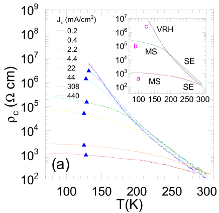
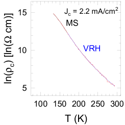
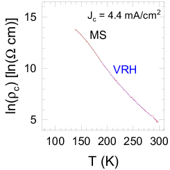
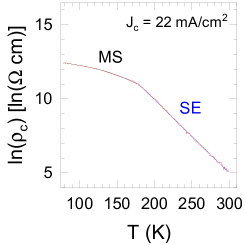
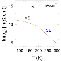
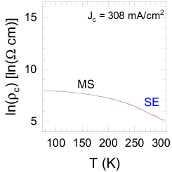
The temperature dependence of the resistivity measured along the c axis for selected values of is reported in semi-logarithmic scale in Fig. 2(a). It is important to notice that analogous results were obtained on all the investigated samples. By increasing , is lowered of up to four orders of magnitude (Okazaki et al., 2013; Sow et al., 2017). Moreover, despite is always a decreasing function of the temperature () (Cao et al., 1997), the shape of the resistivity curves evolves as is increased and distinct behaviors can be observed, as indicated in the inset of Fig. 2(a) by the labels VRH, SE, and MS, which stand for Variable Range Hopping, Semiconducting and Metastable, respectively, as discussed more in detail in the following. In addition, a critical value can be identified, which sets the change in the concavity of the curves in semi-logarithmic scale, in accordance with Ref. (Sow et al., 2017). The curves measured for hardly depend on the value of , as in the case of the ones for and , which completely overlap (Okazaki et al., 2013). By measuring , both lowering and increasing , an irreversible behavior, never reported in the literature, was observed. Indeed, there are portions of the curves whose accessibility depends on the sample history, as shown for example for and . Here the continuous lines indicate the data obtained by lowering . For , the resistance surge beyond the measurable range of the voltmeter at a characteristic temperature, , while for the resistance is still measurable below this value. However, by increasing the temperature from the lowest reached in the experiment, a measurable is detected only for (black dotted lines). The values of are represented as blue triangles in the figure. Interestingly, for all the analyzed crystals and independently on , , a value comparable with . This is the first time that a measure of gives indications of the magnetic ordering temperature in Ca-214 (Cao et al., 1997). Moreover, this result confirms that induces a new more-conductive MS state where AFM is suppressed (Bertinshaw et al., 2019), and, more generally, that can be used to control the magnetic ordering of this class of materials (Sow et al., 2017; Bertinshaw et al., 2019; Sow et al., 2019). A more detailed analysis of this result is beyond the scope of this work and will be subject of future studies.
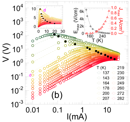
In Fig. 2(b), a selection of characteristics as a function of obtained by biasing the sample along the c axis is shown on a double logarithmic scale. Beyond the low regime, when the samples show a clear insulating behavior, a negative differential resistance is observed (Sakaki et al., 2013; Zhang et al., 2019), in accordance with the dramatic reduction of resistivity observed in the curves by increasing . By further increasing the current, an ohmic dependence, signature of the IMT, is expected (Nakamura et al., 2013). However, this threshold was not exceeded to preserve the crystal integrity and measure the whole resistivity map on the same sample. The change in the conduction results in a maximum in the characteristics at [or equivalently at ], as highlighted in Fig. 2(b) by black circles, both in the main panel and in the inset on the left, where the shape of the curves on a linear scale can be better appreciated. At room temperature and . Their temperature dependence is reported in the right inset of Fig. 2(b). While (black points, left scale) increases with (Nakamura et al., 2013), (red points, right scale) decreases on cooling. This latter behavior is counter-intuitive and requires further analysis to be understood. It is worth noting that should not be confused with . is the value at which, driving with electrical potential, one reaches the thermodynamic metallic phase (M-long) (Nakamura et al., 2013), while is the value at which, driving with , one reaches the MS state.
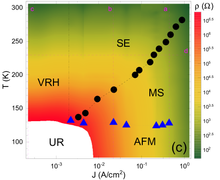 |
By combining both curves measured for different values of and characteristics as a function of , it is possible to draw the contour plot of the crystal resistivity shown in Fig. 3. For the sake of clarity, only a selection of curves, representative of different conduction behaviors, are reported in the Figure as vertical lines (a, b, c), while the same curve labeled as (d) in Fig. 2(b) is represented as an horizontal line (see Fig. 3). The resulting phase diagram comprises different regions, corresponding to different conducting regimes (UR, VRH, SE, MS, and AFM), as marked by the three contours present in the figure. The dot-dashed vertical line represents the value of . The position of the maximum of the curves at the investigated temperature are represented by black dashes [as in Fig. 2(b)]. Finally, the blue dotted line at indicates the non-reversible behavior of the curves, namely the onset of the AFM ordering.
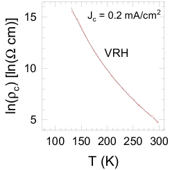
Accordingly, the following conducting regimes are identified. First, in the limit of both low and , there is the so-called Unexplored Region (UR), namely a deeply insulating region which is not accessible due to the limit of used experimental set-up. Then, by moving along the axis (, all ), the has a Variable Range Hopping behavior with a power coefficient of about , typical of 3D systems (for all the details about the fitting of the curves the reader can refer to the Appendix). Here the resistivity is not affected by the bias current density. For , namely by crossing the dot-dashed line, a reduction of is observed (Okazaki et al., 2013). From this side, regions SE and MS, divided by the black dashed line, identify, respectively, the semiconducting and the meta-stable regimes. In region SE (, ), the best fit is obtained by using a decreasing (negative) exponential behavior resembling that of an intrinsic semiconductor at sufficiently high , that is a shallow insulator whose gap is comparable to the temperature range under analysis. In region MS (, ) the has a behavior that is very different from both that of an insulator (decreasing, positive concavity in both linear and log scale) and of a metal (increasing, positive concavity in both linear and log scale), but a decreasing behavior with negative (positive) concavity in log (normal) scale is measured. Indeed, this change of concavity in the log scale allows to identify . Such a situation, still interpreted in the VRH paradigm, marks the divergency of the localization length. This can be interpreted as the signal that at least a portion of the system becomes conducting, leading to a resistivity that strongly resembles those of alloys and whose best fit is obtained with a decreasing (negative) exponential with a power coefficient of about 3. Which is the exact type of conducting mechanism remains to be investigated. The intrinsic dependence on time of the process makes difficult to characterize it through instruments, and related concepts, that are meant to work at equilibrium.
III.2 X-ray diffraction measurements
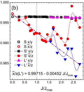
XRD measurements were performed at room by current biasing the crystal to complement the electronic characterization and gain access to the microscopic properties of the different conducting regimes. In Fig. 4(a), the dependence of the c-lattice parameter (left scale) on the normalized current density, , is superimposed to the normalized characteristic (right scale), to allow the comparison among different samples; characteristic level arrangements (I-SC, M’, M-long, see below) are also reported. The values of c were calculated according to the Bragg law by following the position of the reflection of the XRD - scans. The values of the c axis plotted by black-closed circles represent the elongation of the short c axis of the insulating S phase at (, magenta-closed circle) (Nakamura et al., 2013). This change produces a distortion of the lattice cell, which now is labeled as S’. Interestingly, at a new phase indicated as L’, and represented by open circles, clearly emerges. The c axis of L’ also elongates by increasing and is well detectable in the whole investigated current range, which covers the region of negative differential resistance of the curve. Finally, at , the diffraction peak associated with the metallic L phase appears (, black triangle) (Nakamura et al., 2013).
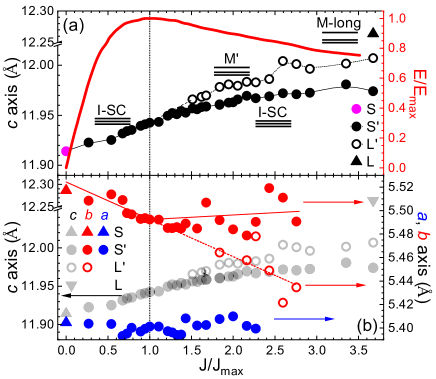
These measurements demonstrate that in the MS state, a new, possibly metallic (L’), crystallographic phase coexists with the short insulating one (S’) in a quite wide range of current values and even with the metallic one (L), at the maximum current reached in the experiment. In panel (b), the dependence on of the lattice parameters a and b, calculated from the position of the reflections and respectively, is compared with the c axis. Noticeably, while the value of the a-axis is almost constant, the b-axis (red dots) splits in two branches at as the c-axis does. In the same region, corresponding to the appearance of the L’ phase, statistical scattering is present in the b-axis data. This can be interpreted as a tentative of the system to release the in-plane strain while trying to accommodate both phases (S’ and L’) in the crystal. From a careful inspection of the data, it also emerges that the statistical scattering of the two phases result overall complementary. It is worth noting that the L’ phase moves towards a metallic tetragonal structure, while the S’ phase slowly relaxes back towards the S one (in terms of crystallographic axis). Indeed, once the L’ phase nucleates and develops, S will sustain only a smaller fraction of the flowing current. It is worth noticing that the values of the lattice parameters, both in the S and in the L phases, are consistent with the results reported in the literature (Braden et al., 1998; Alexander et al., 1999; Nakamura et al., 2013). In particular, the value of the c axis in the metallic phase (L) is in accordance with the ones reported for structural transitions induced by electric field, pressure and temperature (Nakamura et al., 2013). This indicates that, contrary to the MS state, L is a real thermodynamic phase.
IV Discussion
The emergence of a metallic phase (L’) in the system would explain both the puzzling negative differential resistivity of the MS regime and the counter-intuitive increase of with . In fact, in order to sustain a systematic increase of current flow in an overall insulating state, at a certain critical current density, dependent on temperature, and comparable with , the system finds energetically more convenient to nucleate a more conductive crystallographic phase, L’. Consequently, above , the electrical potential needed to further increase the current flow reduces, while the more-conductive L’ phase grows. On increasing , the S’ phase itself can sustain more current, since it becomes less insulating. Accordingly, is an increasing function of . This is just one of the clearest signatures that the emergence of L’ is not a classical effect driven by Joule heating, but that it comes from a much more subtle and complex energy balance.
The remarkable increase of c and decrease of b in L’ phase is definitely compatible with a significant decrease of the ratio that would steadily lead to a metallic behavior of that portion of the material. To check this hypothesis, a transformation matrix computed in Ref. (Han and Millis, 2018) by means of DFT+U calculations was used. This allows to track the effect of applied strain on a, b and c and, in particular, as this reflects on , and (see Appendix). The obtained related changes of , and give, as expected, a decreasing ratio of , following the evolution with increasing current from S’ to L’, but also two unpredictable results: first, above , that is, once L’ sets in, S’ goes back towards the values of , and characteristics of S; second, the decrease of is mainly determined by the decrease of and not by the increase of . Once the system has the possibility to fully exploit the L’ phase to allow an increasingly current flow, S’ phase can relax back to S one. The complicated intertwining of rotation, tilt and distortion maps the increase of c mainly on a reduction of than on an increase of .
V Conclusions
In summary, dc current drive was used to determine the phase diagram. By profiting of a new protocol, it was possible to access a region of the phase diagram not yet explored and to unveil the nucleation and evolution of a new metallic crystallographic phase, L’, completely compatible with the transport data. Its corresponding cell dimensions depart from those of the insulating short phase and approach those of the metallic long phase. The main octahedral axis and the corresponding levels of the new phase were theoretically obtained: the phase L’ is more conducting than S’ and can be considered as a precursor of the metallic L phase.
Such findings explain the unexpected and counterintuitive results of the transport data and completely determine the behavior in the metastable phase. Such findings are consistent with the literature, and represent a significant improvement of the current comprehension of a complex system such as Ca-214, opening new perspectives in its microscopic characterization. These results open new perspectives in the microscopic characterization of Ca-214. For instance, spectroscopic measurements under electrical current drive may represent a valuable validation of the present findings.
Acknowledgements.
The authors gratefully acknowledge Y. Maeno and G. Mattoni for the useful discussions and I. Nunziata for technical support.Appendix A XRD data supplement
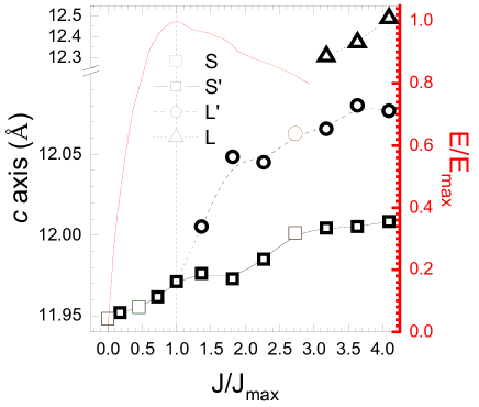
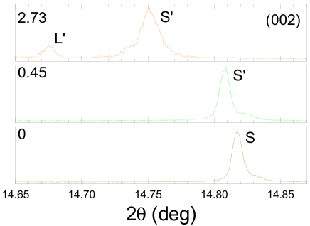
In order to provide further evidence of the coexistence of the three distinct crystallographic phases in the current induced meta-stable state, additional XRD data for another single crystal are presented in Fig. 5. Here the values of the c-lattice parameters as a function of the normalized electrical current density were derived from the reflection. Again the comparison with the normalized curve measured for the same crystal (right scale) confirms that the S’ phase splits into the L’ phase at (see vertical dashed line). This new phase is well distinguishable in all the investigated current range from the other two diffraction peaks, as shown in Fig. 6, where three representative - scans of the reflection are reported for different values of corresponding to different regions of the characteristic. It is evident that before reaching the maximum of the characteristic, namely in the insulating regime, only the peaks identifying the phases S and S’ are present (dark yellow and green scans, respectively). Above , the diffraction peak of the L’ phase develops, as shown by the orange line, acquired at .
Appendix B Theoretical methods
 |
 |
 |
B.1 octahedra
 |
 |
 |
 |
 |
 |
 |
 |
B.1.1 Crystal field
The complex is an octahedron whose vertices are occupied by atoms and its center by a atom. Such a type of - coordination, according to the Jahn-Teller effect (Khomskii, 2014), splits the levels of the in two groups: , and , and , , and . In the first group, , the orbitals have lobes pointing directly towards the directional orbitals of and therefore lie higher in energy. On the other hand, in the second group, , the actual distances of the apical oxygens , in the main text, and of the in-plane oxygens , and in the main text (and their average), determine the degree of degeneracy of the three levels: a perfect octahedron () leads to three perfectly degenerate levels. Instead, the smaller is with respect to (at fixed the higher in energy lies the level with respect to ; as well as the smaller is with respect to the higher in energy lies the level with respect to the - doublet.
As schematically reported in Fig. 1(b) in the main text, the order in energy of the levels is fundamental to establish how the four electrons per present in the system decide to occupy such levels. As a consequence, this determines the transport properties of the related state. In the I-short state, and is lower in energy with respect to the - doublet with a crystal field gap that can be so large that the electrons prefer to arrange in pairs in level although the local Coulomb repulsion would avoid that. The remaining two electrons can accommodate in the - doublet according to the Hund’s rule with parallel spins and such a configuration, at low enough temperatures, leads to an insulating antiferromagnetic state. At higher temperatures, since gets closer and closer to the levels become almost degenerate. In this situation, the strong correlations prevent the system to behave as a metal, but still as an insulator, by splitting the and levels in lower and upper Mott-Hubbard bands. By further increasing the temperatures, become sufficiently larger than to have the - doublet below the level and lead to a metal. In this case, three electrons fill in the levels according to the Hund’s rule and one electron gets free to move in the lattice.
B.1.2 Crystallographic axes vs distances
By means of DFT+U calculations, A. Millis and coworkers (Han and Millis, 2018) found a transformation matrix relating the variations of the crystallographic axis , and to the variations of the distances in the octahedra, that is, , and :
| (1) |
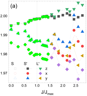
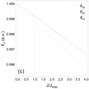
where , and . This matrix allows one to find the values of , , and given those of , and for the the two phases, S’ and L’, emerging from the S one on applying an electrical current drive [see Fig. 7(a)]. It was then possible to obtain the two fundamental ratios and in the S’ and L’ phases [see Fig. 7(b)]. A least-squares linear fit of the ratio for the L’ phase (following the one of the S’ phase for ) resulted very accurate and the related fit parameters are reported directly in the figure [see Fig. 7(b)]. Given the almost constant ratio and the linear fit of the ratio , it has been possible to compute the relative energies of the , and levels [see Fig. 7(c)]. This supports our interpretation that the unconventional and puzzling behavior of the meta-stable state are due to the emergence of the metallic phase L’ in the system.
B.2 Conductive regimes: VRH, SE and MS
All the curves reporting the behavior of the resistivity as a function of the temperature , for different values of , have been least-squares fitted with the same generic allometric function (see Fig. 8):
| (2) |
According to the sign of and the value of , it is possible to identify three distinct conducting regimes (VHR, SE and MS) which set in a specific range of temperatures depending on the value (see Tabs. 1-3). The values of have been chosen according to the closest value for all currents and temperatures in the regime in order to avoid excessive fluctuations in the other parameters.
It is worth noting that such unbiased fits of the R(T) curves independently and accurately reproduce the position of the maximum in the I-V characteristics.
| () | () | A | ||
|---|---|---|---|---|
| All | ||||
| All | ||||
B.2.1 Variable Range Hopping (VRH)
In this case, it is and . The results of the fitting procedure reported in Tab. 1 are compatible with a 3D system.
() () A () Table 2: Meta-Stable regime fitting parameters
B.2.2 Meta-Stable (MS)
In this case, it is and . In Tab. 2 the fitting parameters corresponding to the MS regime are reported. is the equivalent activation temperature.
() () () Table 3: Semiconductor regime fitting parameters
B.2.3 Semiconductor (SE)
In this case, it is and . The fitting procedure returns the values reported in Tab. 3. is the activation temperature.
References
- Gorelov et al. (2010) E. Gorelov, M. Karolak, T. O. Wehling, F. Lechermann, A. I. Lichtenstein, and E. Pavarini, Phys. Rev. Lett. 104, 226401 (2010).
- Sow et al. (2017) C. Sow, S. Yonezawa, S. Kitamura, T. Oka, K. Kuroki, F. Nakamura, and Y. Maeno, Science 358, 1084 (2017).
- Riccò et al. (2018) S. Riccò, M. Kim, A. Tamai, S. McKeown Walker, F. Y. Bruno, I. Cucchi, E. Cappelli, C. Besnard, T. K. Kim, P. Dudin, M. Hoesch, M. J. Gutmann, A. Georges, R. S. Perry, and F. Baumberger, Nat. Commun. 9, 4535 (2018).
- Das et al. (2018) L. Das, F. Forte, R. Fittipaldi, C. G. Fatuzzo, V. Granata, O. Ivashko, M. Horio, F. Schindler, M. Dantz, Y. Tseng, D. E. McNally, H. M. Rønnow, W. Wan, N. B. Christensen, J. Pelliciari, P. Olalde-Velasco, N. Kikugawa, T. Neupert, A. Vecchione, T. Schmitt, M. Cuoco, and J. Chang, Phys. Rev. X 8, 011048 (2018).
- Porter et al. (2018) D. G. Porter, V. Granata, F. Forte, S. Di Matteo, M. Cuoco, R. Fittipaldi, A. Vecchione, and A. Bombardi, Phys. Rev. B 98, 125142 (2018).
- Steffens et al. (2005) P. Steffens, O. Friedt, P. Alireza, W. G. Marshall, W. Schmidt, F. Nakamura, S. Nakatsuji, Y. Maeno, R. Lengsdorf, M. M. Abd-Elmeguid, and M. Braden, Phys. Rev. B 72, 094104 (2005).
- Mizokawa et al. (2001) T. Mizokawa, L. H. Tjeng, G. A. Sawatzky, G. Ghiringhelli, O. Tjernberg, N. B. Brookes, H. Fukazawa, S. Nakatsuji, and Y. Maeno, Phys. Rev. Lett. 87, 077202 (2001).
- Sutter et al. (2017) D. Sutter, C. G. Fatuzzo, S. Moser, M. Kim, R. Fittipaldi, A. Vecchione, V. Granata, Y. Sassa, F. Cossalter, G. Gatti, M. Grioni, H. M. Rønnow, N. C. Plumb, C. E. Matt, M. Shi, M. Hoesch, T. K. Kim, T.-R. Chang, H.-T. Jeng, C. Jozwiak, A. Bostwick, E. Rotenberg, A. Georges, T. Neupert, and J. Chang, Nat. Commun. 8, 15176 (2017).
- Nakatsuji and Maeno (2001) S. Nakatsuji and Y. Maeno, J. Solid State Chem. 156, 26 (2001).
- Cao et al. (1997) G. Cao, S. McCall, M. Shepard, J. E. Crow, and R. P. Guertin, Phys. Rev. B 56, R2916 (1997).
- Nakamura (2007) F. Nakamura, J. Phys. Soc. Jpn. 76, 96 (2007).
- Alireza et al. (2010) P. L. Alireza, F. Nakamura, S. K. Goh, Y. Maeno, S. Nakatsuji, Y. T. C. Ko, M. Sutherland, S. Julian, and G. G. Lonzarich, J. Phys. Condens. Matter 22, 052202 (2010).
- Carlo et al. (2012) J. P. Carlo, T. Goko, I. M. Gat-Malureanu, P. L. Russo, A. T. Savici, A. A. Aczel, G. J. MacDougall, J. A. Rodriguez, T. J. Williams, G. M. Luke, C. R. Wiebe, Y. Yoshida, S. Nakatsuji, Y. Maeno, T. Taniguchi, and Y. J. Uemura, Nat. Mater. 11, 323 (2012).
- Sutter et al. (2019) D. Sutter, M. Kim, C. E. Matt, M. Horio, R. Fittipaldi, A. Vecchione, V. Granata, K. Hauser, Y. Sassa, G. Gatti, M. Grioni, M. Hoesch, T. K. Kim, E. Rienks, N. C. Plumb, M. Shi, T. Neupert, A. Georges, and J. Chang, Phys. Rev. B 99, 121115(R) (2019).
- Nakamura et al. (2013) F. Nakamura, M. Sakaki, Y. Yamanaka, S. Tamaru, T. Suzuki, and Y. Maeno, Sci. Rep. 3, 2536 (2013).
- Braden et al. (1998) M. Braden, G. André, S. Nakatsuji, and Y. Maeno, Phys. Rev. B 58, 847 (1998).
- Zhang and Pavarini (2017) G. Zhang and E. Pavarini, Phys. Rev. B 95, 075145 (2017).
- Kikuzuki and Lippmaa (2010) T. Kikuzuki and M. Lippmaa, Appl. Phys. Lett. 96, 132107 (2010).
- Rini et al. (2007) M. Rini, R. Tobey, N. Dean, J. Itatani, Y. Tomioka, Y. Tokura, R. W. Schoenlein, and A. Cavalleri, Nature 449, 72 (2007).
- Ehrke et al. (2011) H. Ehrke, R. I. Tobey, S. Wall, S. A. Cavill, M. Först, V. Khanna, T. Garl, N. Stojanovic, D. Prabhakaran, A. T. Boothroyd, M. Gensch, A. Mirone, P. Reutler, A. Revcolevschi, S. S. Dhesi, and A. Cavalleri, Phys. Rev. Lett. 106, 217401 (2011).
- Ichikawa et al. (2011) H. Ichikawa, S. Nozawa, T. Sato, A. Tomita, K. Ichiyanagi, M. Chollet, L. Guerin, N. Dean, A. Cavalleri, S.-i. Adachi, T.-h. Arima, H. Sawa, Y. Ogimoto, M. Nakamura, R. Tamaki, K. Miyano, and S.-y. Koshihara, Nat. Mater. 10, 101 (2011).
- Okazaki et al. (2013) R. Okazaki, Y. Nishina, Y. Yasui, F. Nakamura, T. Suzuki, and I. Terasaki, J. Phys. Soc. Jpn. 82, 103702 (2013).
- Janod et al. (2015) E. Janod, J. Tranchant, B. Corraze, M. Querré, P. Stoliar, M. Rozenberg, T. Cren, D. Roditchev, V. T. Phuoc, M.-P. Besland, and L. Cario, Adv. Funct. Mater. 25, 6287 (2015).
- Imada et al. (1998) M. Imada, A. Fujimori, and Y. Tokura, Rev. Mod. Phys. 70, 1039 (1998).
- Limelette et al. (2003) P. Limelette, A. Georges, D. Jérome, P. Wzietek, P. Metcalf, and J. M. Honig, Science 302, 89 (2003).
- Zhang et al. (2019) J. Zhang, A. S. McLeod, Q. Han, X. Chen, H. A. Bechtel, Z. Yao, S. N. Gilbert Corder, T. Ciavatti, T. H. Tao, M. Aronson, G. L. Carr, M. C. Martin, C. Sow, S. Yonezawa, F. Nakamura, I. Terasaki, D. N. Basov, A. J. Millis, Y. Maeno, and M. Liu, Phys. Rev. X 9, 011032 (2019).
- Bertinshaw et al. (2019) J. Bertinshaw, N. Gurung, P. Jorba, H. Liu, M. Schmid,D.T Mantadakis,M. Daghofer,M. Krautloher, A. Jain, G. H. Ryu, O. Fabelo, P. Hansmann, G. Khaliullin, C. Pfeiderer, B. Keimer, and B. J. Kim, Phys. Rev. Lett. 123, 137204 (2019).
- Sow et al. (2019) C. Sow, R. Numasaki, G. Mattoni, S. Yonezawa, N. Kikugawa, S. Uji, and Y. Maeno, Phys. Rev. Lett. 122, 196602 (2019).
- Fukazawa et al. (2000) H. Fukazawa, S. Nakatsuji, and Y. Maeno, Physica B 281-282, 613 (2000).
- Sakaki et al. (2013) M. Sakaki, N. Nakajima, F. Nakamura, Y. Tezuka, and T. Suzuki, J. Phys. Soc. Jpn. 82, 093707 (2013).
- Alexander et al. (1999) C. S. Alexander, G. Cao, V. Dobrosavljevic, S. McCall, J. E. Crow, E. Lochner, and R. P. Guertin, Phys. Rev. B 60, R8422 (1999).
- Han and Millis (2018) Q. Han and A. Millis, Phys. Rev. Lett. 121, 067601 (2018).
- Khomskii (2014) D. I. Khomskii, Transition Metal Compounds (Cambridge University Press, 2014).