text]text
Nondegenerate Two-Photon Absorption in GaAs/AlGaAs Multiple Quantum Well Waveguides
Abstract
We present femtosecond pump-probe measurements of the nondegenerate ( nm excitation and – nm probe) two-photon absorption spectra of GaAs/ nm Al0.32Ga0.68As quantum well waveguides. Experiments were performed with light pulses co-polarized normal and tangential to the quantum well plane. The results are compared to perturbative calculations of transition rates between states determined by the method with an 8 or 14 band basis. We find excellent agreement between theory and experiment for normal polarization, then use the model to support predictions of orders-of-magnitude enhancement of nondegenerate two-photon absorption as one constituent photon energy nears an intersubband resonance.
pacs:
Valid PACS appear hereI Introduction
Nondegenerate two-photon absorption (ND-2PA) is a process whereby absorption of an optical field is induced by a second, high irradiance field at a different wavelength. Applications of ND-2PA include detection Fishman et al. (2011), imaging Pattanaik et al. (2016a), and all-optical switching Liang et al. (2005). Inverting carrier populations can also transform ND-2PA into nondegenerate two-photon gain Reichert et al. (2016); Melzer et al. (2018); Hayat et al. (2008), which is critical for realizing a two-photon semiconductor laser Ironside (1992); Gauthier et al. (1992); Hayat et al. (2011). Waveguides are especially interesting for nonlinear optical applications because they enable strong effects through long interaction lengths. Group velocity mismatch (GVM) induced walkoff usually limits nondegenerate interactions, but dispersion engineering can mitigate or remove this walkoff entirely Poulvellarie et al. (2018).
The degenerate 2PA (D-2PA) spectrum of infinite quantum wells was first predicted by Spector (1987) and Pasquarello and Quattropani (1988). Shortly after, Nithisoontorn et al. (1989) experimentally demonstrated D-2PA to excitons in GaAs quantum wells. Shimizu (1989) developed an excitonic model for D-2PA, and Tai et al. (1989) verified their predictions with two-photon luminescence spectra. Later, Yang et al. (1993) showed the anisotropy of D-2PA in quantum well waveguides.
Pasquarello and Quattropani (1990) relaxed some of Shimizu’s approximations and extended the analysis to nondegenerate photon pairs, predicting large enhancements as one photon energy neared an intersubband resonance. Pattanaik et al. (2016b) quantitatively examined these nondegenerate resonance enhancements, expanding upon a six-band theory developed by Khurgin (1994).
Here, we present the first pump-probe measurements of ND-2PA coefficients in GaAs quantum wells. We studied nm GaAs/ nm Al0.32Ga0.68As quantum wells at room temperature using beams polarized normal (TM-TM) and tangential (TE-TE) to the quantum well plane, and compared the results with a theoretical model for ND-2PA in finite wells neglecting excitonic effects.
We find that our perturbative model matches experimental results very closely for TM-TM beams, whereas a relatively large error in TE-TE predictions indicates that a more thorough analysis is needed. The TM-TM model shows that predictions of intersubband resonance enhancements of ND-2PA also apply to finite wells, suggesting the possibility of extremely sensitive gated detection of sub-bandgap pulses Fishman et al. (2011).
This article is organized as follows. In Sec. II, we derive a method for calculating ND-2PA coefficients in an arbitrary quasi-2D semiconductor. We introduce our GaAs quantum well waveguide in Sec. III and describe the pump-probe experiments carried out to find its ND-2PA coefficients. In Sec. IV, we apply the model of Sec. II to a simple quantum well structure that approximates our sample. Measurement results are presented in Sec. V followed by a discussion in Sec. VI.
Appendix A contains background information about the Kane band structure model for zinc blende semiconductors. Appendix B shows the derivation of an intersubband matrix element in the envelope function expansion. In Appendix C, we give the equations and parameters used in numerical simulations of quantum well states and optical modes. Appendix D contains nonlinear wave propagation analysis, as well as the techniques used to match the calculation results to experimental curves. Less essential equation derivations are placed in the supplemental material Sup .
II Theoretical Background
The -th level wave function of the -th band (e.g. conduction, heavy hole, light hole) in a semiconductor confined in the direction is Chuang (1995)
| (1) |
is an envelope with lattice periodicity only in , the component tangential to the quantum well plane.
Second order perturbation theory gives the net two-photon transition rate per unit volume Lee and Fan (1974)
| (2) |
where and are conduction and valence envelopes, respectively. is the interaction Hamiltonian for a vector potential of magnitude and polarization , given by Basov et al. (1966)
| (3) |
The term arises from the chain rule for the momentum operator applied to states in the form of Eq. (1). This term is usually ignored because it frequently cancels out, but we leave it in for completeness.
The transition rate is converted to an ND-2PA coefficient by Sheik-Bahae and Van Stryland (1999)
| (4) |
which describes the attenuation of wave at frequency induced by wave at . and are the incident field irradiances
| (5) |
with the effective index at . We also introduce a unitless matrix element between envelopes Hutchings and Van Stryland (1992)
| (6) |
As detailed in Appendix A, the Kane parameter is the optical coupling strength between conduction and valence bands.
Finally, we combine Eqs. (II)–(6) into a general expression for ND-2PA coefficients: Sup
| (7) |
where is the dimensionless spectral function
| (8) |
The quantity is the bandgap of the quantum well material and is the Kane energy. The parameter is the total thickness of the structure in the direction. For a single quantum well, is the sum of the barrier and well widths.
Eq. (7) is valid in any unit system so long as the material-independent parameter is adjusted accordingly. With energies and lengths written in Hartree atomic units (), this constant is simply . The final 2PA coefficient can then be converted to cm/GW by the conversion factor .
The integral in Eq. (II) is taken over the azimuthal angle of , whose magnitude has been replaced by the unitless quantity . Energies are also normalized by letting and . Each is a real, positive solution to
| (9) |
We derived Eqs. (7) and (II) without making any assumptions of specific band structure or layer design, leaving us with a general expression for ND-2PA coefficients in quasi-2D materials. Later, we make approximations to simplify calculations for the symmetric quantum wells introduced in the next section.
III Sample and Experiment
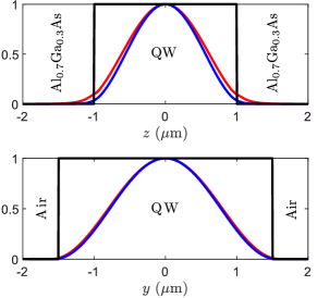
We experimentally investigated GaAs quantum wells MBE-grown by Sandia National Laboratories on an n-GaAs (100) substrate. A wave guiding structure was formed in the direction by growing thick Al0.7Ga0.3As cladding layers on either side of a active region. The active region comprised repetitions of ( GaAs)/( Al0.32Ga0.68As) quantum wells, with barrier widths chosen so that coupling between wells is negligible. Transverse optical confinement was achieved by etching a wide ridge through the active region and lower cladding. Finally, the sample was cleaved to a length of . The layer structure and geometry are seen in Fig. 1.
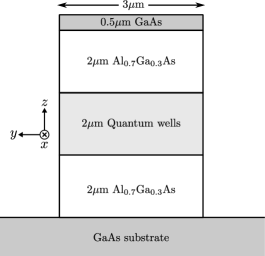
Fig. 2 shows the optical setup employed to study the sample. A short wavelength probe and long wavelength pump came from the signal and idler, respectively, of a Spectra-Physics OPAL optical parametric oscillator (OPO) synchronously driven by a Spectra-Physics Tsunami Ti:Al2O3 laser with MHz repetition rate. We tuned the driving laser wavelength between and to study 2PA at sum photon energies near the absorption edge. For each driving laser wavelength, the OPO phase matching was adjusted to fix the idler at . In effect, the pump was fixed at while the probe varied between and . This pump photon energy was chosen to be below the D-2PA edge so that two-photon photogenerated carriers did not interfere with data interpretation.
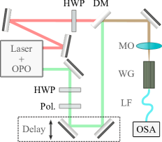
After fixing the signal and idler wavelengths, their polarizations were set to TE (-polarized) or TM (-polarized) using broadband half-wave plates. The probe then traveled through a delay line and combined with the pump at a dichroic mirror. The beams were end-fire coupled into the ridge waveguide (Fig. 1) using a microscope objective and collected by a lensed fiber at the exit facet. The lensed fiber was connected to a Yokogawa AQ6370D spectrum analyzer (OSA in Fig. 2) to compare the probe output power spectrum with and without the pump’s presence. The process was repeated at a series of probe delays to generate curves of normalized transmission versus delay.
It is necessary to know the pump power at the facet inside the waveguide to convert normalized transmission to an ND-2PA coefficient. This input power was calculated by back-propagating the OSA-measured output power to the front facet using
| (10) |
which depends on the waveguide loss , the sample propagation length , and the the output facet coupling efficiency . This efficiency was experimentally determined by temporarily replacing the microscope objective of Fig. 2 with a lensed fiber identical to the one at the output. By measuring for this symmetric system, we found the facet transmission by
| (11) |
After finding a waveguide loss of and (See Appendix D), we determined the transmission coefficients of the front facet to be and .
Autocorrelation measurements of the pump at four different sum wavelengths gave the following pulsewidths: at , at , at , and at . By comparing to the measured spectra, we determined pump pulsewidths to be an average of greater than the Gaussian bandwidth limit.
IV Calculation of 2PA coefficients
This section describes the model used to calculate the 2PA coefficients of a symmetric GaAs quantum well. We begin by calculating the energy levels and envelope functions of each subband level. Then we construct expressions for the optical matrix elements between all states. Finally, Eq. (II) is used to calculate the 2PA coefficients for parabolic bands.
IV.1 Wavefunction envelopes
Calculation of ND-2PA coefficients requires knowledge of the energy levels and wave functions between which two-photon transitions occur. We begin by expanding the envelope functions in the basis of zone center wavefunctions : Luttinger and Kohn (1955); Bastard (1981)
| (12) |
The basis is chosen to consist of either 8 or 14 spin-degenerate bands (see Appendix A for details). For ease of calculation, we only solve for envelopes at ; the approximation applied for is discussed later in this subsection. Taking the alloy composition-dependent energy offset of band as a z-dependent potential leads to a second order Schrödinger Equation Bastard (1976)
| (13) |
The superscript on denotes the dominant envelope, and is the state’s energy-dependent effective mass in the direction. Choosing the 8 band basis for Eq. (12) yields the effective mass relation Bastard (1976); Sup
| (14) |
The quantity is the spin-orbit split-off energy and are remote band contributions included by Löwdin’s perturbation method Löwdin (1951). We take the approximation that this remote band contribution is independent of energy.
In the 14 band basis, the conduction band effective mass changes to Sup
| (15) |
where is the light electron band at and is the split-off electron band at . is the coupling energy between the two sets of conduction bands. All hole effective masses are identical to the 8 band results.
If we set and in Eqs. (IV.1) and (IV.1), we find expressions for bulk GaAs effective masses. As was done in Ref. Meney et al. (1994), we choose so that calculated bulk effective masses match experimental values.
We assume the band dispersion to have the form
| (16) |
where is the effective mass in the transverse direction. This parabolic band approximation has been successfully used to calculate 2PA coefficients for bulk semiconductors Basov et al. (1966), at the cost of ignoring some fine structure in the dispersion Hutchings and Van Stryland (1992).
IV.2 Matrix Elements
Equipped with a model for electronic states, we can proceed to calculate the optical matrix elements between them. Two-photon transitions across the bandgap always require an interband transition, for which we consider allowed and forbidden paths. For TM-TM polarizations, the remaining step is assumed to be an allowed intersubband transition. In TE-TE 2PA, the remaining step is assumed to be a forbidden self transition Wherrett (1984). These two interaction types vary differently with wavelength near the 2PA edge, causing anisotropy between the polarization schemes.
Intersubband matrix elements are calculated between the envelopes found from Eq. (13). As a consequence, the results are only strictly valid at the band edge. For TM polarization, we find that
| (17) |
where
| (18) |
See Appendix B for justification of the above equation. This form exhibits two improvements over that in Refs. Pattanaik et al. (2016b) and Khurgin (1994), viz. . The first is to include energy scaling of the effective mass, and the second is to account for the fact that interband coupling depends only on the inverse effective mass component arising from interactions within the basis. Eq. (17) can also be compared to that in Ref. [Seechapter4of]Faist2013, which ignores the subtraction of remote band contributions.
Self transitions are forbidden because they describe optical coupling between states of nearly identical symmetry. Eq. (17) with shows that these contributions are negligible for TM polarization. For TE fields we use the relation Ashcroft and Mermin (1976) with the energy given by Eq. (16). Fixing TE polarization in the direction leads to
| (19) |
Eq. (17) is also valid for interband transitions, but using it would ignore the dependence once again. Instead, we use the method of Yamanishi and Suemune (1984) to estimate matrix elements from the bulk band structure:
| (20) |
where is the zone-center basis function for band . As described in Appendix A, the prime denotes that the basis functions are rotated by an angle . We find from the energy relation . Eq. (20) applies to TM and TE polarizations and accounts for allowed () and forbidden () transitions.
IV.3 2PA coefficients for Parabolic Bands
The energy separation between parabolic conduction and valence bands is given in normalized form by
| (21) |
where and . We see immediately from Eq. (21) that
| (22) |
Combining Eqs. (9) and (21), we find
| (23) |
Feeding the results of Eqs. (21)–(23) into Eq. (II) gives a general expression for the dimensionless scaling factor in the parabolic band approximation:
| (24) |
The sum runs only over conduction states, with identical transitions included by a factor of . The step function defines the range where the solution of Eq. (23) is real. The aforementioned angular rotation factor in the interband matrix element is found to be
| (25) |
Two-photon absorption coefficients can finally be found from Eq. (7). Note that each quantum well is treated as a separate system so that in this equation is the total thickness of a single well (20 nm).
Eq. (IV.3) is valid for TM-TM, TE-TE and the mixed-polarization TE-TM configurations. Because the co-polarized schemes provide sufficient information about the ND-2PA anisotropy, we do not perform the less tractable cross-polarized calculations. The next two subsections provide some simplifications for the TM-TM and TE-TE cases.
IV.3.1 TM-TM 2PA coefficients
As shown in Fig. 3, every TM-TM two-photon transition includes one interband and one intersubband transition. Because envelope parity alternates with subband index, the required TM matrix element (Eq. (17)) imposes the selection rule for integer . Since every element in Table 1 is independent of , the azimuthal integral of Eq. (IV.3) reduces to unity such that
| (26) |
Both matrix elements are non-zero at the ND-2PA edge for doubly-allowed transitions, giving the step-like shape characteristic of linear quantum well absorption.

IV.3.2 TE-TE 2PA coefficients
Per Fig. 3, each TE-TE 2PA path involves an interband and a self transition. Two-photon transitions therefore inherit the selection rules of the the interband transition, namely . Using the matrix elements from Table 2, which are generally -dependent, we simplify the dimensionless scaling function to
The term linear in grows from zero at the 2PA edge, meaning TE-TE 2PA dispersion lacks the discontinuities seen in TM-TM 2PA curves.
| Eq. (17) | |||
| Eq. (17) | |||
| Eq. (17) | |||
The integration has been reduced to the average over a single term denoted with angular brackets. Performing the integration for each pair of bands gives
| (28) |
Note that if we chose polarized light, we would need to use the components of the interband matrix elements and take . The result is that the integration over yields identical values to polarized light. This equivalence is consistent with the fact that physical measurements must have the azimuthal symmetry of the isotropic bands.
V Results
Normalized transmission versus pump-probe delay was measured as described in Sec. III, and coupled nonlinear Schrödinger equations were used to fit the curves to ND-2PA coefficients. The exact procedure is detailed in Appendix D, along with all necessary approximations and empirical adjustments.
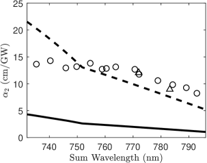
TM-TM measurement results are plotted versus sum wavelength in Fig. 4 alongside theoretical predictions. Sum wavelength is defined by , where the pump wavelength is fixed at 1960 nm. Excitations of light hole states bring about discontinuities in the spectrum, with the and transitions accounting for the shorter and longer wavelength steps, respectively. In contrast with light hole contributions, heavy hole signals exhibit a gradual increase due to the interband matrix element’s (forbidden) dependence. Each transition’s onset is found by subtracting the subband energies in Table 4 of Appendix C using the selection rule .

.
Expanding states in the 8 band basis with eV Hermann and Weisbuch (1977), our predicted curve matched the data apart from a nm wavelength shift. This offset is mitigated by using the 14 band model with Hermann and Weisbuch (1977). In both cases, we assumed there were small growth errors such that the real material consisted of nm wells with Al0.328Ga0.672As barriers. The effect of this modification is revealed by comparing the blue (solid) and magenta (dotted) curves of Fig. 4. Other sources for this wavelength inaccuracy could be OSA miscalibration or the use of imprecise bandgap values in simulations, but these assumptions lead to curves nearly identical to the ones shown.
Interestingly, calculated 2PA coefficients vary significantly with the value chosen for the Kane energy. This sensitivity is apparent when comparing the 14 band theoretical curve with another that has and Hermann and Weisbuch (1977). By the arguments of Sec. IV.1, under these conditions we require so that Eq. (IV.1) reduces to the bulk effective mass for GaAs. For comparison, when eV. This modification reduces the intersubband matrix element according to Eq. (17).
Fig. 5 shows the TE-TE results compared with 14 band calculations. The ND-2PA edge is energetically lower than in TM-TM because it first occurs for transitions, leading to large anisotropy below the TM-TM transition energy. The theoretical curve, which is smooth with a kink at m from transitions, shows this anisotropy. However, our unscaled calculations differ from the measurements by over a factor of four and show some dissimilarity in shape. We provide reasons for these differences in the following section.
VI Discussion
The TM-TM theory matches the data without any non-physical scaling parameter; this excellent agreement is likely due to the dominance of allowed transitions. The parabolic band approximation works well because important features in the 2PA spectrum occur at small , where the parabolic band approximation introduces little error. Calculations show that the ND-2PA coefficients measured here are enhanced by a factor of over degenerate 2PA.
We do not notice any bound excitonic response, which may be attributed to temperature effects. Continuum exciton enhancement is also not evident. Ref. Shimizu (1989) concludes that this contribution is absent in Ref. Tai et al. (1989) due to low sample quality and large exciton spatial extent. We suspect the same reasons apply here, with further reductions possibly occurring due to loss of 2-D character from interactions between many closely spaced wells.
In contrast to TM-TM polarizations, the parabolic band approximation introduces significant errors in TE-TE ND-2PA coefficients. By ignoring unit cell intermixing, we underestimate the -dependent scaling of forbidden transitions that are necessary in TE-TE pathways. We also determine that it is insufficient to examine only self-transitions as the forbidden step; we must also consider intersubband transitions and those between different hole types. Away from the band edge, light hole to heavy hole transitions were shown to be non-negligible for 2PA in bulk semiconductors Hutchings and Van Stryland (1992). TE-TE coefficients could be more accurately calculated by numerically computing the highly non-parabolic band dispersion as in Ref. Chuang (1991). Eq. (6) would then give matrix elements throughout the Brillouin zone, which are used to find 2PA coefficients according to Eq. (II).
The sensitivity of the 2PA coefficient to Kane energy and effective masses indicates that pump probe spectroscopy of quantum wells may be an effective method for determining basic material parameters. Our results, while not precise enough to justify a definitive declaration, seem to support the idea that the Kane energy is closer to eV than lower values that have been reported (See Appendix C). Furthermore, Hübner et al. (2009) and others have shown evidence that the Kane energy is dependent on temperature. With better spectral resolution and careful experimental setup, the temperature dependence of could be reflected both in a magnitude change of the normalized transmission signal and a shift of the ND-2PA edge as effective mass is changed (See Eq. (39)).
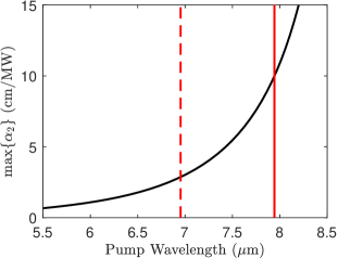
With this experimental support for our model, we can re-examine ND-2PA for extremely nondegenerate photon pairs Pattanaik et al. (2016b); Cirloganu et al. (2011); Pasquarello and Quattropani (1990). Fig. 6 shows that the calculated TM-TM ND-2PA coefficients rapidly increase as the pump wavelength nears the resonance at m. The red vertical lines denote points where the probe energy for maximum 2PA lies within meV of the forbidden (dashed, ) and allowed (solid, ) linear absorption edges. The offset value is chosen so that we can roughly assume negligible impurity state absorption, but these edges will shift depending on material quality and temperature. For m, we see that cm/MW—an enhancement of over the slightly nondegenerate case studied here, and a considerably larger ND-2PA coefficient than any we have measured in bulk semiconductors (cm/MW) Cirloganu et al. (2011). This enhancement suggests the possibility of extremely sensitive gated detection as in Ref. Fishman et al. (2011), with even further increases in photogenerated carrier density due to long pulse interactions within a waveguide.
Acknowledgements.
Funding for NC, DH, and EVS was provided by National Science Foundation grant DMR-1609895 and the Army Research Laboratory (W911NF-15-2-0090). This work was performed, in part, at the Center for Integrated Nanotechnologies, an Office of Science User Facility operated for the U.S. Department of Energy (DOE) Office of Science by Los Alamos National Laboratory (Contract 89233218CNA000001) and Sandia National Laboratories (Contract DE-NA-0003525). JW and SPG acknowledge the support from the Fonds de la Recherche Fondamentalei Collective (FRFC) (PDR.T.1084.15).Appendix A Kane Band Structure
Kane (1957) developed a band structure model for bulk zinc blende materials using a formalism including spin-orbit interaction. The unit cell basis consisted of two spin-degenerate -like functions and with energy and six degenerate -like functions , , , , , and with . By symmetry of the zincblende crystal, all non-zero momentum matrix elements are given by Yu and Cardona (2010)
| (29) |
The wave vector in bulk materials is not restricted to two dimensions as in quantum wells. In Ref. Kane (1957), the Hamiltonian is diagonalized in a rotated coordinate system for which . This coordinate transformation is represented as a 3-dimensional rotation matrix since , and transform as the components of a vector Yu and Cardona (2010). Finally, the k-dependent eigenstates are found to be
| (30) |
The heavy hole bands () are uncoupled while the conduction, light hole, and split off bands—denoted by index —intermix. The primed kets indicate rotated basis functions.
The zone center () unit cell functions are listed in Table 3. Taking the first four and states gives the 8 band Kane basis described above. The more complete 14 band model includes conduction bands at energy and , with representing spin-orbit splitting in the conduction bands. These two sets are used as bases for the envelope expansion in Eq. (12).
| E | |
|---|---|
Interband matrix elements
Comparing the of Eq. (A) to the zone center values in Table 3, we note they differ by the expansion coefficients as well as a rotation of basis functions. As in Ref. Yamanishi and Suemune (1984), we assume quantum well transitions are adequately described by using the zone center expansion coefficient while applying the basis rotation. For example, , which evaluates to the value given in Table 1 after application of Eqs. (29) and (20).
Appendix B Intersubband Matrix Element
This appendix derives the intersubband matrix element in Eq. (17). The procedure shown is for conduction bands in the 8 band basis, but it is easily generalized to other bands and different basis sets.
The momentum matrix element between states given in the envelope expansion (Eq. (12)) is
| (31) |
where we have chosen to represent inner products with operator as for clarity. As usual, . We apply the chain rule for the differential operator , then assume and change on different enough scales so that we can integrate their expressions separately. In atomic units we find
| (32) |
where values are obtained from Eq. (29) and Table 3. Suppose now that the intial and final envelopes are conduction states. We can express the non-dominant envelopes as a function of the conduction envelope by
| (33) |
These substitions appear in Ref. Bastard (1976), and are re-derived in detail in the supplemental material Sup . Applying Eqs. (B) to Eq. (B) gives
| (34) |
where we dropped the subscript on the right hand side. We also used the fact that . Noting that in atomic units, comparing to Eq. (IV.1) immediately leads to
| (35) |
Normalization and conversion back to bra-ket notation gives Eq. (17). This process can be easily repeated for hole transitions and states written in the 14 band basis.
Appendix C Simulation parameters and procedures
Since we are not working with an idealized structure, we must employ some numerical techniques to model our systems. In the first subsection of this appendix, we calculate energy levels and envelopes for states in the finite quantum well. In the second, we find the optical mode structure and dispersion characteristics of the waveguide.
C.1 Material simulations
We first give the bandgap of GaAs and the composition-dependent bandgap of AlGaAs in order to determine the confining potential imposed by the AlGaAs barriers. Then we provide values for interband couplings and effective masses, followed by a brief summary of the calculation results. Each value is taken from literature, making adjustments as needed.
The temperature-dependent bandgap of GaAs is given by the Varshni relation Varshni (1967)
| (36) |
with and El Allali et al. (1993); Vurgaftman et al. (2001). The higher conduction band energies in the 14 band model are taken to be eV and eVCardona et al. (1967).
The potential barriers imposed by the quantum well layer structure come from the empirical expression for total band offset between GaAs and AlxGa1-xAs:El Allali et al. (1993)
| (37) |
The ratio Vurgaftman et al. (2001) at an AlxGa1-xAs interface, simplifying conduction and valence offsets to
| (38) |
All hole types are presumed to have offset and all conduction bands are taken to have offset .
Literature values for the Kane energy of GaAs vary between Balslev (1969), Lawaetz (1971), Pfeffer and Zawadzki (1996), Eppenga et al. (1987) and Hermann and Weisbuch (1977). We choose , and take the inter-conduction band coupling strength as Hermann and Weisbuch (1977).
The conduction band effective mass of GaAs is Vurgaftman et al. (2001) at room temperature. Light hole masses are anisotropic with Vrehen (1968) as determined from cyclotron resonance at . This mass is adjusted to its room temperature value by
| (39) |
where temperature-dependent bandgaps are taken from Eq. (36). This relation comes from subtracting the Eq. (IV.1) expressions for K and K. The final outcome is that .
The energy-dependent effective mass is calculated in the 8 band model using Eq. (IV.1) with spin-orbit splitting of Aspnes and Studna (1973).
The heavy hole effective mass is Chuang (1995)
| (40) |
where is the AlGaAs composition at position . The symbol is the six-band Luttinger parameter linearly interpolated between the values for GaAs and AlAs Vurgaftman et al. (2001):
| (41) |
Transverse hole effective masses are also taken from the Luttinger parameters as Chuang (1995)
| (42) | ||||
| (43) |
With all material parameters known, the shooting method Harrison and Valavanis (2005) is used to solve Equation . The procedure yields the energy level (See Table 4) and dominant wavefunction envelope for each state. Note that the material widths and compositions are slightly altered as explained in Sec. V.
| c | lh | hh | |
|---|---|---|---|
| – | – |
C.2 Waveguide Modes
Refractive index values for the various AlGaAs compositions used were calculated by Adachi’s formulas Adachi (1989). The index of the quantum well active region was estimated to be the spatial average of the well () and barrier () permittivities
| (44) |
Using these indices, electromagnetic mode profiles and dispersion curves were calculated from the finite difference method with Lumerical MODE Solutions Lum . The mode shapes are shown in Fig. 7.
The third order mode areas and overlap were calculated in the usual way Lin et al. (2007):
| (45) |
| (46) |
where is the electric field profile of mode . The calculated TM (TE) mode area at was found to be (), and the TM (TE) probe mode areas range from () at to () at . The mode overlap at and was , so they are treated as unity. Due to tight optical confinement within the active region, propagation is well-approximated by taking modes to travel through a material entirely made up of the quantum wells.
We numerically differentiated the refractive index curves to find group velocities and second order dispersions. The largest GVM of fs/mm occurred when and , with the pump travelling faster than the probe. Around this value, fs pulses walk off from each other on the length scale of . The largest dispersion coefficient of occurs at the same probe wavelength, while the pump dispersion is at nm. These values were used in the simulations of Appendix D.
Appendix D Nonlinear propagation and data fitting
We modeled pulse propagation by the coupled nonlinear Schrodinger equations Agrawal (2012)
| (47) |
| (48) |
is the instantaneous power, and are the first and second order dispersion, and is the loss. We neglect free carrier contributions to the nonlinear propagation because the pulses have sufficiently low average power such that excited carrier density is negligible. The nonlinear parameter is written in terms of the mode areas and overlap as Lin et al. (2007)
| (49) |
We set because the pump wavelength is below the D-2PA edge, and the are ignored because the probe power is low. All nonlinear refraction effects from are ignored, which is justified in the following subsection.
Raw data and analysis
Fig. 8 shows a normalized transmission signal generated as described in Sec. III. A delay of zero indicates that the pump and probe arrive at the front facet at the same time, and a negative delay means the probe arrives before the pump. The curve is temporally wider than the input pulses because the faster moving pump overtakes the probe within the sample for delays up to about ps.
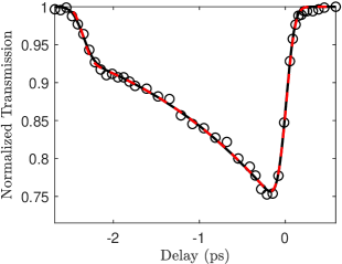
Transmission curves in high GVM experiments usually exhibit a table top shape like those in Ref Cirloganu et al. (2011). Instead, we see a decay in the nonlinear transmission magnitude as delay becomes more negative. This indicates that loss in pump irradiance leads to a smaller signal as the pulses meet after propagating farther through the sample. If these losses were caused by an interband absorption process, there would be a constant signal at positive delay due to excited carrier interactions. Instead, we attribute this decay to high scattering from roughness of the etched sidewall.
The shape of Fig. 8 is explained by the analytical expression for normalized transmission Sup
| (50) |
Here, is the length of the sample and is the total energy of the pump pulse. The value is the pure cross correlation width between pulse durations , and is the GVM parameter. Eq. (D) was derived by ignoring second order dispersion. Despite this approximation, we see by comparing the curves in Fig. 8 that the equation yields nearly identical results to those found by split-step Fourier integration of Eqs. (D) and (D) with non-zero .
The insensitivity to is related to an overall pulse width insensitivity of the normalized transmission. Qualitatively, the increase in pump irradiance at fixed energy due to decrease in pulsewidth is compensated by a decrease in interaction length as the pulses walk through each other. In fact, with , the maximum signal of Eq. (D) is completely independent of pulse widths. Since the linear and nonlinear pulse broadening should be negligible over the walkoff length, this independence would be true without ignoring and . In our case, altering the pulsewidth only causes a slight signal reduction due to a delay shift in the curve moving the peak back to a point where more pump losses have occurred. This only gives an error of around when is underestimated by a factor of two. We use this insensitivity to justify ignoring nonlinear refraction in Eqs. (D) and (D).
Data fitting procedure
For TM-TM (TE-TE) sum wavelengths of , , , (, , ) the transmission curves were fit with , , and as free parameters. Averaging the resulting loss coefficents gives and . A wavelength shift of was applied to the dispersion curve so the simulated values of more closely match the fits. This adjusment is needed most likely due to the inaccuracy of the spatially averaged approximation to the quantum well index (Eq. (44)). The values presented here were held fixed in fitting the rest of the data.
The rest of the data points in Figs. 4 and 5 were found by measuring the rising edge and peak of the normalized transmission. The pump pulsewidth was taken to be greater than the bandwidth limit (see Sec. III), and and were free fitting parameters. Once again, the effect of this imperfect knowledge of pulsewidths is mitigated by the signal’s insensitivity to pulse width. The and GVM values were held fixed according to the previous fitting procedure.
References
- Fishman et al. (2011) D. A. Fishman, C. M. Cirloganu, S. Webster, L. A. Padilha, M. Monroe, D. J. Hagan, and E. W. Van Stryland, Nature Photonics 5, 561 (2011).
- Pattanaik et al. (2016a) H. S. Pattanaik, M. Reichert, D. J. Hagan, and E. W. Van Stryland, Optics Express 24, 1196 (2016a).
- Liang et al. (2005) T. K. Liang, L. R. Nunes, T. Sakamoto, K. Sasagawa, T. Kawanishi, M. Tsuchiya, G. R. A. Priem, D. Van Thourhout, P. Dumon, R. Baets, and H. K. Tsang, Optics Express 13, 7298 (2005).
- Reichert et al. (2016) M. Reichert, A. L. Smirl, G. Salamo, D. J. Hagan, and E. W. Van Stryland, Physical Review Letters 117, 073602 (2016).
- Melzer et al. (2018) S. Melzer, C. Ruppert, A. D. Bristow, and M. Betz, Optics Letters 43, 5066 (2018).
- Hayat et al. (2008) A. Hayat, P. Ginzburg, and M. Orenstein, Nature Photonics 2, 238 (2008).
- Ironside (1992) C. N. Ironside, IEEE Journal of Quantum Electronics 28, 842 (1992).
- Gauthier et al. (1992) D. J. Gauthier, Q. Wu, S. E. Morin, and T. W. Mossberg, Physical Review Letters 68, 464 (1992).
- Hayat et al. (2011) A. Hayat, A. Nevet, P. Ginzburg, and M. Orenstein, Semiconductor Science and Technology 26 (2011).
- Poulvellarie et al. (2018) N. Poulvellarie, C. Ciret, B. Kuyken, F. Leo, and S. P. Gorza, Physical Review Applied 10, 24033 (2018).
- Spector (1987) H. N. Spector, Physical Review B 35, 5876 (1987).
- Pasquarello and Quattropani (1988) A. Pasquarello and A. Quattropani, Physical Review B 38, 6206 (1988).
- Nithisoontorn et al. (1989) M. Nithisoontorn, K. Unterrainer, S. Michaelis, N. Sawaki, E. Gornik, and H. Kano, Physical Review Letters 62, 3078 (1989).
- Shimizu (1989) A. Shimizu, Physical Review B 40, 1403 (1989).
- Tai et al. (1989) K. Tai, A. Mysyrowicz, R. J. Fischer, R. E. Slusher, and A. Y. Cho, Physical Review Letters 62, 1784 (1989).
- Yang et al. (1993) C. C. Yang, A. Villeneuve, G. I. Stegeman, C. H. Lin, and H. H. Lin, IEEE Journal of Quantum Electronics 29, 2934 (1993).
- Pasquarello and Quattropani (1990) A. Pasquarello and A. Quattropani, Physical Review B 42, 9073 (1990).
- Pattanaik et al. (2016b) H. S. Pattanaik, M. Reichert, J. B. Khurgin, D. J. Hagan, and E. W. Van Stryland, IEEE Journal of Quantum Electronics 52, 1 (2016b).
- Khurgin (1994) J. B. Khurgin, Journal of the Optical Society of America B 11, 624 (1994).
- (20) See Supplemental Material at [URL will be inserted by publisher] for derivations of the ND-2PA coefficient formula, energy-dependent effective masses, and the analytical expression for nonlinear propagation.
- Chuang (1995) S. L. Chuang, Physics of Optoelectronic Devices (Wiley, 1995).
- Lee and Fan (1974) C. C. Lee and H. Y. Fan, Physical Review B 9, 3502 (1974).
- Basov et al. (1966) N. G. Basov, A. Z. Grasyuk, I. G. Zubarev, V. A. Katulin, and . N. Krokhin, J. Exptl. Theoret. Phys. (U.S.S.R.) 23, 551 (1966).
- Sheik-Bahae and Van Stryland (1999) M. Sheik-Bahae and E. W. Van Stryland, in Nonlinear Optics in Semiconductors I (Elsevier Masson SAS, 1999) Chap. 4, pp. 257–318.
- Hutchings and Van Stryland (1992) D. C. Hutchings and E. W. Van Stryland, Journal of the Optical Society of America B 9, 2065 (1992).
- Luttinger and Kohn (1955) J. M. Luttinger and W. Kohn, Physical Review 97, 869 (1955).
- Bastard (1981) G. Bastard, Physical Review B 24, 5693 (1981).
- Bastard (1976) G. Bastard, Wave Mechanics Applied to Semiconductor Heterostructures (Wiley-Interscience, 1976).
- Löwdin (1951) P. O. Löwdin, The Journal of Chemical Physics 19, 1396 (1951).
- Meney et al. (1994) A. T. Meney, B. Gonul, and E. O’Reilly, Physical Review B 50, 893 (1994).
- Wherrett (1984) B. S. Wherrett, Journal of the Optical Society of America B 1, 67 (1984).
- Faist (2013) J. Faist, Quantum cascade lasers (Oxford University Press, 2013).
- Ashcroft and Mermin (1976) N. W. Ashcroft and N. D. Mermin, Solid State Physics (Cengage, 1976).
- Yamanishi and Suemune (1984) M. Yamanishi and I. Suemune, Japanese Journal of Applied Physics 23, 35 (1984).
- Hermann and Weisbuch (1977) C. Hermann and C. Weisbuch, Physical Review B 15, 823 (1977).
- Chuang (1991) S. L. Chuang, Physical Review B 43, 9649 (1991).
- Hübner et al. (2009) J. Hübner, S. Döhrmann, D. Hägele, and M. Oestreich, Physical Review B - Condensed Matter and Materials Physics 79, 1 (2009).
- Cirloganu et al. (2011) C. M. Cirloganu, L. A. Padilha, D. A. Fishman, S. Webster, D. J. Hagan, and E. W. Van Stryland, Optics Express 19, 22951 (2011).
- Kane (1957) E. O. Kane, Journal of Physics and Chemistry of Solids 1, 249 (1957).
- Yu and Cardona (2010) P. Y. Yu and M. Cardona, Fundamentals of semiconductors (Springer, New York, 2010).
- Varshni (1967) Y. Varshni, Physica 34, 149 (1967).
- El Allali et al. (1993) M. El Allali, C. B. Sorensen, E. Veje, and P. Tidemand-Petersson, Physical Review B 48, 4398 (1993).
- Vurgaftman et al. (2001) I. Vurgaftman, J. R. Meyer, and L. R. Ram-Mohan, Journal of Applied Physics 89, 5815 (2001).
- Cardona et al. (1967) M. Cardona, K. L. Shaklee, and F. H. Pollak, Physical Review 154, 696 (1967).
- Balslev (1969) I. Balslev, Physical Review 177, 1173 (1969).
- Lawaetz (1971) P. Lawaetz, Physical Review B 4, 3460 (1971).
- Pfeffer and Zawadzki (1996) P. Pfeffer and W. Zawadzki, Physical Review B 53, 12813 (1996).
- Eppenga et al. (1987) R. Eppenga, M. H. Schuurmans, and S. Colak, Physical Review B 36 (1987).
- Vrehen (1968) Q. H. F. Vrehen, Journal of Physics and Chemistry of Solids 29, 129 (1968).
- Aspnes and Studna (1973) D. E. Aspnes and A. A. Studna, Physical Review B 7, 4605 (1973).
- Harrison and Valavanis (2005) P. P. Harrison and A. Valavanis, Quantum wells, wires and dots, 2nd ed. (Wiley, Sussex, England, 2005).
- Adachi (1989) S. Adachi, Journal of Applied Physics 66, 6030 (1989).
- (53) “Lumerical MODE Solutions,” .
- Lin et al. (2007) Q. Lin, O. J. Painter, and G. P. Agrawal, Optics Express 15, 16604 (2007).
- Agrawal (2012) G. P. Agrawal, Nonlinear Fiber Optics (Academic Press, 2012) p. 631.