Diversified properties of carbon substitutions in silicene
Abstract
The theoretical framework, which is built from the first-principles results, is successfully developed for investigating emergent two-dimensional (2D) materials, as it is clearly illustrated by carbon substitution in silicene. Computer coding with the aid of VASP in conjunction with data analysis from the multi-orbital hybridizations [spin configurationsf ] are thoroughly identified from the optimal honeycomb lattices, the atom-dominated energy spectra, and the spatial charge density distributions. The atom and orbital-decomposed van Hove singularities [the net magnetic moments], being very sensitive to the concentration and arrangements of guest atoms. All the binary 2D silicon-carbon compounds belong to the finite- or zero-gap semiconductors, corresponding to the thoroughly/strongly/slightly modified Dirac-cone structures near the Fermi level. Additionally, there are frequent and band crossings, but less anti-crossing behaviors. Apparently, our results indicate the well-defined and bondings.
Keywords: buckled structure, silicene, substitution, geometric structure, electronic properties.
* Corresponding author. Tel: +886-6-2757575-65272
E-mail address: mflin@mail.ncku.edu.tw (M.F. Lin)
1. Introduction
Chemical substitutions on layered materials are capable of band structure tailoring which could lead to significant modifications of the properties of pristine lattices through very strong host-guest multi-orbital hybridizations. With the use of modern experimental growth techniques, ternary and binary compounds, which are characterized by BxCyNz, have been successfully synthesized for three-dimensional (3D) bulk systems [1, 2], two-dimensional (2D) layers [3], one-dimensional (1D) cylindrical nanotubes [4], 1D nanoribbons [5], and zero-dimensional (0D) quantum dots [6]. Their geometric structures vary from three to zero dimensions, as observed in carbon-related systems [7, 8]. This clearly indicates that each atom possesses at least three half-filled orbitals. Similar syntheses have been performed for the high-potential Si-C compounds [9]. In general, it would be routine to produce the above-mentioned compounds, whereas the opposite might be true for specific components. For example, using high-performance experimental techniques, it may be difficult to manipulate the ratio between the [B, C, N]/[Si, C] atoms. Such non-monoelement condensed-matter systems have been predicted or found to exhibit the observable energy gaps, or belong to specific semiconductors. The main reason lies in the distinct ionization energies of their components, being consistent with the tight-binding mode for non-vanishing diagonal Hamiltonian matrix elements [the sublattice-dependent site energies]. Gap engineering could be achieved by transforming the strength relations in the , and sp3 bondings the [pz-, (s, px, py)- and (s, px, py, pz)-orbital hybridizations].
Chemisorption and substitution of silicon atoms on graphene are two very interesting procedures, since first-principles predictions are available for understanding the important differences between these two types of chemical modification [10, 11], and providing additional information regarding another approach for the formation of silicon-carbide compounds [12]. Based on the viewpoint of a carbon-created honeycomb lattice, silicon atoms are regarded as adatoms and guest ones, respectively, in these two cases. The former presents optimal positions at the bridge sides above the graphene surface [13], while the latter shows the [Si, C]-co-dominated A and B sublattices with deformed hexagons [14]. Both silicon and carbon atoms have rather active dangling bonds, leadings to significant multi-orbital hybridizations in Si-C [Si-Si and C-C] bonds. Most important, the planar bondings between Si and C atoms are expected to be stronger and complicated, compared with the perpendicular configuration. That is to say, the and [] bondings of graphene will be significantly modified by Si-substitutions [15]. This is directly reflected in the diversified properties, the spatial charge distributions, atom-dominated energy bands, and atom- as well as orbital-projected density-of-states. Furthermore, their gradual transformations could be achieved through the Si-/C-substituted graphene/silicene honeycomb lattice.
The present work is focused on the diverse geometric, electronic and magnetic properties of C-substituted silicene. A theoretical framework, which is based on multi-orbital hybridizations and atom-created spin configurations, is further developed to clearly analyze the concentration- and configuration-dependent phenomena. For example, the zero- and finite-gap behaviors, the main features of and bands could be understood from the specific relations among the hybridized , and sp3 chemical bondings. On the experimental side, a controllable synthesis way, using MTMS/hexane as precursors, is proposed to generate the large-area graphene-based Si-C binary 2D compounds [16]. Furthermore, the silicon-carbide nanosheets are successfully synthesized by a catalyst free carbothermal method and post-sonication process [17], in which the AFM measurements show the average thickness of nm and size of m.
2. Method of calculation
Our investigation of the diverse properties of carbon-substituted silicene is base on density functional theory using VASP codes [18, 19]. The exchange and correlation energies due to many-particle Coulomb interactions were calculated with the use of the Perdew-Burke-Ernzerhof (PBE) functional under the generalized gradient approximation [20], whereas the electron-ion interactions can be characterized by the projector augmented wave (PAW) pseudopotentials [21]. A plane-wave basis set with a maximum kinetic energy cutoff of 500 eV was chosen to expand the wave function. In a direction perpendicular to the silicene plane, a vacuum layer with a thickness of 15 was added to avoid interactions between adjacent unit cells. The k-point mesh was set as in geometry optimization, for further calculations on electronic properties via the Monkhorst-Pack scheme. During the ionic relaxations, the maximum Hellmann-Feynman force acting on each atom is less than eV/ whereas the convergent energy scale was chosen as eV between two consecutive steps.
3. Numerical Results and discussion
0.1 Geometric structure of carbon-substituted silicene
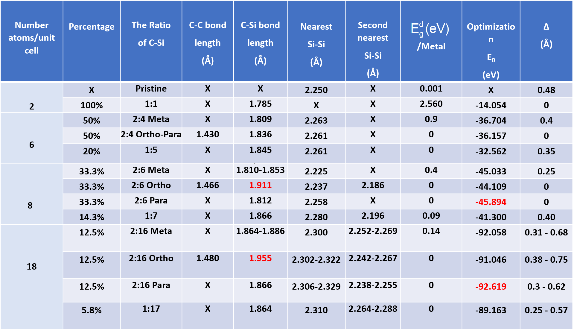
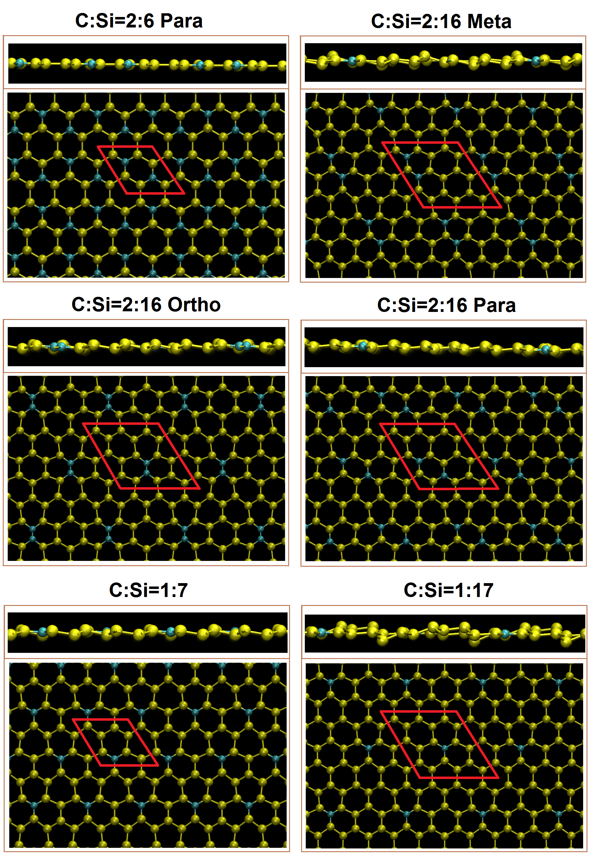
Carbon-substituted silicon systems are capaable of possessing unusual geometries, as it is clearly indicated in Table 1 and Figs. 2(a) through 2(l). Four types of typical C-substitution configurations, which cover meta, ortho, para, and single cases, are chosen for a model investigation. In general, the third and fourth types, respectively, possess the lowest and highest ground state energies, i. e., the para-configuration is the most stable among them, or it is expected to be relatively easily synthesized in experimental growths. Carbon and silicon atoms, respectively, possess four outer orbitals of [2px, 2py, 2pz, 2s] and [3px, 3py, 3pz, 3s]. In addition to the pure ones, the substitutions of the former, as clearly illustrated in Fig. 2(a) through 2(l), will create the hybridized and bondings [2pz-3pz and (2s, 2px, 2py)-(3s, 3px, 3py)] in silicene honeycomb lattice [the standard orbital hybridizations in Fig. 2(a)]. This seems to be responsible for the extremely non-uniform chemical/physical environments in an enlarged unit cell. Consequently, the Si-Si/Si-C bond lengths and the height difference between A and B sublattices might lie in specific ranges [Table 1]. Specifically, the full C-substitution case, with the only uniform environment, is clearly different from the pristine one, since they, respectively, have the planar and buckled honeycomb lattices [Figs. 2(b) and 2(a); =0 ]. When the C-concentration is sufficiently low, the buckled structures will recover, such as, the C:Si ratio lower than 15. For the other conditions, the existence of buckling strongly depends on the concentration and configuration of the substitution.
![[Uncaptioned image]](/html/1912.00334/assets/9-1.png)
0.2 Band structure tailoring of Carbon-substituted silicene systems
The specific relations among the , and bondings in a pristine monolayer silicene account for the main features of the band structure. The electron-hole symmetry around the Fermi level is only weakly modified at low energy, as illustrated in Fig. 3(a). The first pair of valence and conduction bands. being nearest to , are initiated from the stable K/K′ valley. A very narrow band gap of meV comes to exist between slightly separated Dirac cones, mainly due to the weak spin-orbital coupling [a single-particle interaction]. This result is consistent with that obtained using the tight-binding model [22]. Additionally, they show the valence/conduction saddle M-point structure at -1.02 eV/0.59 eV. Finally, the band is ended at the stable valley, in which the -band energy width for valence states, the energy spacing between the initial K point and the final point is about 3.2 eV. Apparently, such electronic spectrum originates from the bonding of pure 3-3 orbital hybridizations in the buckled honeycomb lattice. On the other hand, the four-fold degenerate bands, which arise mainly from [3px, 3]-orbital bondings, obey parabolic energy dispersion relations from the stable valley at eV. The and valence bands have the obvious or observable mixing behavior along the K and M directions, since there exists a weak, but significant sp3 bonding. Additionally, the band width of the first -electronic states along MK is about 3.45 eV. Generally, all - and -bands [three-band] widths could be well defined for monolayer silicene. In addition, all -states in the energy bands are doubly degenerate in terms of spin degree of freedom, since the spin-up- and spin-down-dominated states have identical energy spectra.
![[Uncaptioned image]](/html/1912.00334/assets/9-3.png)
The full carbon-substitution silicene system, i.e., the silicon-carbon binary compound [23], exhibits an unusual electronic energy spectrum as shown in Fig. 3(b), being totally different from the pristine case [Fig. 3(a)]. The occupied valence bands are highly asymmetric to the unoccupied conduction bands near . Such material is classified as a direct-gap insulator with a band gap larger than 2.56 eV at the K/K′ point, as observed in a wide-gap monolayer boron-nitride system [24]. This is closely related to the strongly modified Dirac-cone structure across the Fermi level with highly anisotropic enegy dispersions [e.g., the partially flat conduction band along KM]. Both valence and conduction bands nearest to are, respectively, and bands due to the - impure orbital hybridizations in Si-C bonds. The higher/lower ionization energy of 2pz/3pz orbitals further leads to the creation of a band gap for the honeycomb lattice, and the C-/Si-dominance of the / bands [the red and blue circles]. The first pair of energy bands are highly anisotropic. For example, the valence/conduction / states, which are initiated from the K valley, show different group velocities along the KM and K directions, especially for the saddle point/the partially flat dispersion related to the M point. Furthermore, the -band energy width is eV] according to the difference between the K- and -point energies [ eV and eV. Compared with a pristine 3pz-3pz case [ eV in Fig. 3(a)], the larger band width might indicate the stronger 2pz-3pz bonding. The two bands, which arise from [3px, 3py]-[2px, 2py] hybridizations, appear at eV initiated from the point, but remain fourfold degenerate electronic states there. Furthermore, the contributions from the different orbitals are comparable in the [C, Si]-co-dominated energy bands. The concave-downward parabolic valley near the point is dramatically transformed into cancave-upward ones/the saddle-point forms along the K/M direction. Consequently, the first -bandwidth is approximately eV. There exist direct crossings of the and valence bands along any direction, e.g., M and K. This result clearly reveals no evidence of sp3 bonding [25]. As a result, the fundamental properties of the [1:1] Si-C compound are dominated by the well-behaved and bondings in the absence of sp3 ones.
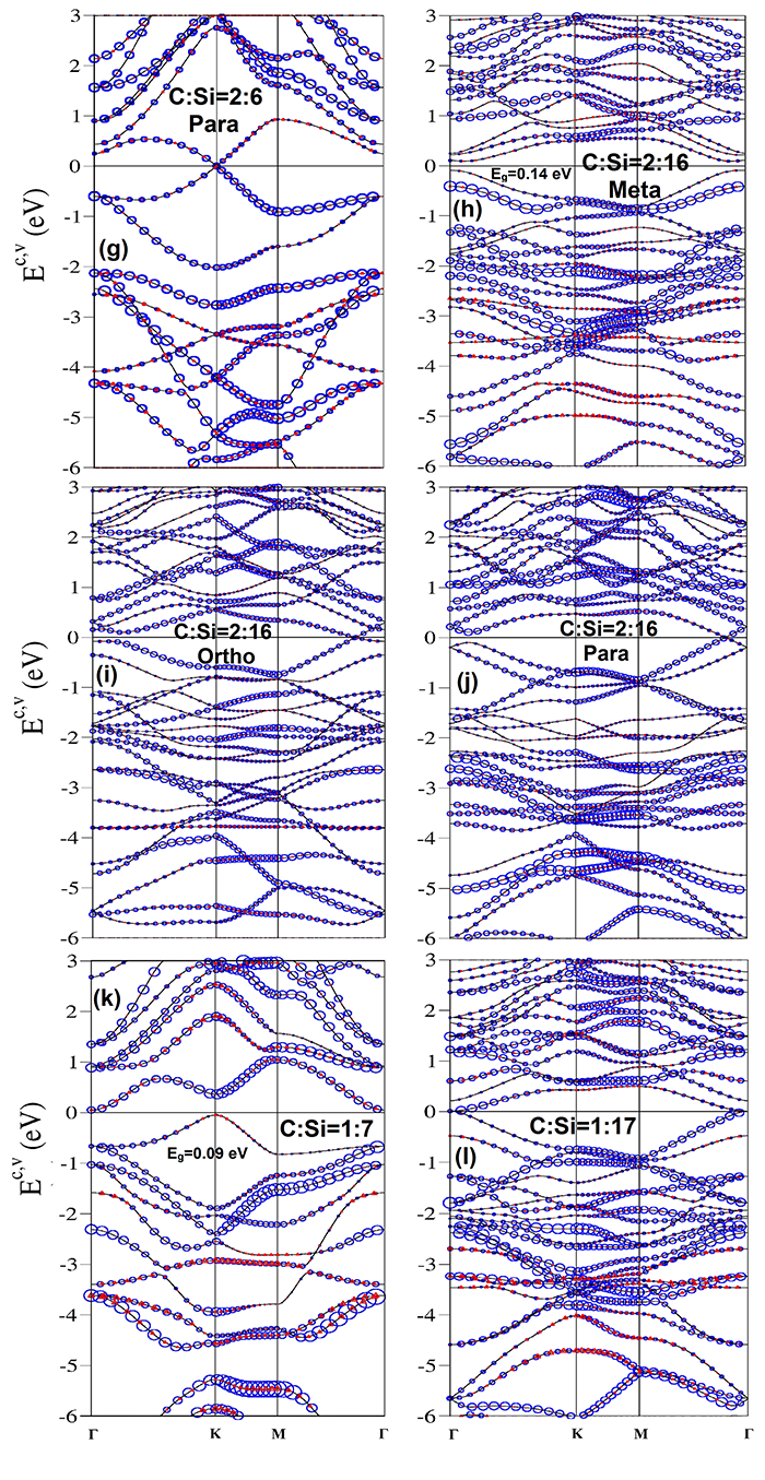
Electronic energy spectra are greatly enriched through the modulations of concentration and distribution configuration. The [2:4]-meta and [2:4]-ortho/para cases, as clearly displayed in Figs. 3(c) and 3(d), present finite- and zero-gap behaviors, respectively, corresponding to the highest occupied state and lowest one at the point [ eV] and the gapless Dirac-cone structure along the K direction [but not M]. That the low-lying valence and conduction bands are initiated from the stable valley is associated with the zone-folding effect. According to the pristine and full-substitution configurations [Figs. 3(a) and 3(b)], the valence and conduction bands in the energy range of eV, including the first pair, mainly arise from the [2pz, 3pz]-orbital hybridizations. Such bondings are responsible for the low-energy physical properties. This result is also confirmed by the orbital-projected density-of-states [discussed later in Fig. 5(b)]. It should be noted that the latter [Fig. 3(d)] belongs to a zero-gap semiconductor because of the vanishing density-of- states at the Fermi level. The low-lying energy bands are dominated by the 3pz orbitals of silicon-host atoms because of the higher weight. More energy subbands come to exist under the enlarged unit cells. Therefore, the band crossings and anti-crossings would happen frequently. In addition, it might be able to define the -band energy widths through the KKMM direction [examinations from the 3pz-projected density-of-states in Figs. 5(c) and 5(d)], respectively, corresponding to eV and eV for the meta- and ortho-configurations. It would be very difficultm or even meaningless, in characterizing band widths with further decrease of guest-atom concentration, as a result of more complicated valence subbbands. Concerning the first valence bands, they are roughly identified from the initial -states at eV for the meta-case [Fig. 3(c)], while the very strong zone-folding effects forbid their characterizations under the ortho-condition [Fig. 3(d)].
Very interestingly, two kinds of band properties are also revealed in the [2:6] cases, as clearly indicated in Figs. 3(e)-3(g). The meta-, ortho- and para-configurations, respectively, exhibit the small-, narrow- and zero-gap behaviors [the finite- and zero-gap semiconductors] according to the first pair of energy bands nearest to the Fermi level. The first case has an indirect band gap of eV, being determined by the specific energy spacing between the highest occupied state at the K point and the lowest unoccupied state at the point [Fig. 3(e)]. Furthermore, the first valence band has an oscillatory energy dispersions. As a result, two stable valleys dominate low-energy physical phenomena simultaneously. The significant overlaps of valence and conduction bands, which come to exist along any wave vector direction, appear under the second configuration in Fig. 3(f). There are five/three energy subbands, with weak oscillatory dispersion relations near the point/ the K and M points. They are responsible for the formation of partially flat bands and thus the high density-of-states near the Fermi level [discussed later in Fig. 5(f)]. The third case in Fig. 3(g) shows a gapless Dirac cone structure at the K/K′ valley only with a single Fermi momentum state [a zero density-of-states at in Fig. 5(g)]]. There are more finite energy spacings between valence and conduction subbands at the valley. For any guest-atom configurations, most electronic energy spectra are dominated by the silicon atoms, while the opposite is true for the carbon atoms.
Clearly, there appear more complex electronic energy spectra when the guest-atom concentrations are decreased [under the reduced/enhanced number of Si-C and C-C/Si-Si bonds]. Typically, three sorts of distribution configurations are revealed under the specific [2:16] condition, the meta-, ortho-, and para-ones in Figs. 3(h) through 3(j). Their low-lying band structures exhibit strongly modified Dirac cones, respectively, with a direct gap of eV due to parabolic valence and conduction dispersion relations near the valley, the gapless and crossing structure [the finite energy spacing] along the M direction [the K direction], and similar zero-gap behavior. Additionally, the single [1:7] substitution in Fig. 3(l) creates an eV indirect band gap associated with the valence K state and conduction state. It should be emphasized that the second and third electronic structures only belong to zero-gap semiconductors [the vanishing density-of-states at in Figs. 5(i) and 5(j)]. The Moiré superlattices have created a substantial number of energy subbands within a smaller first Brillouin zones, leading to frequent band crossings and anti-crossings. As a consequence, it is very difficult to characterize the -band width [similarly for the bandwidths. However, the orbital-projected density-of-states might be useful in examining the relationship among the , and sp3 bondings. Interestingly, C-substituted silicene will gradually recover to the pristine case [Fig. 3(a)] at very low guest-atom concentrations, e.g., the appearance of an almost gapless Dirac cone under the [1:17] case in Fig. 3(l). In summary, the energy subbands, with eV, are dominated by the [2pz, 3pz] orbital hybridization, and the other deeper-/higher-energy electronic states might be closely related to the [2px, 2py, 2s, 3px, 3py 3s] or eight orbitals in Si and C atoms. The carbon substitutions in silicene can only induce the modified Dirac cone structures, but not free carriers [the - or -type dopings].
High-resolution angle-resolved photoemission spectroscopy (ARPES) measurements provide a convenient way for examining/identifying occupied electronic energy spectra along specific 2D/1D wave vector directions. This technique has identified several unusual low-lying energy dispersion relations in graphene-related sp2-bonding materials, such as, the linear valence Dirac cone in monolayer graphene [26], two pairs of parabolic bands in bilayer AB stacking [27], partially flat, sombrero-shape and linear energy bands in trilayer ABC stacking [28], bilayer-/monolayer-like energy bands of Bernal graphite at the K/H corners [AB-stacked one at /; [29], and 1D parabolic energy subbands of graphene nanoribbons [30], The delicate and thorough ARPES examinations are required for the predicted band structures of C-substituted silicene materials. That is, they cover the zero- and finite-gap behaviors with the modified Dirac-cone structures across the Fermi level/without the carrier dopings, the band/subbands with the initial K or valley, the intermediate saddle-M-point form the final valley, the degenerate bands initiated at deeper energies from the valley, their band crossings anti-crossings along the K and M directions, and spin-degenerate electronic states, being very sensitive to the configuration and concentration of guest atoms [Figs. 3(a) through 3(l)]. The full information about the verified band structures is very useful in understanding the substitution-enriched relations among the , and sp3 bondings in Si-Si, Si-C and C-C chemical bonds, and the non-magnetic property.
The first-principles calculations acknowledge that the tight-binding model is capable of simulating the low-lying spin-degenerate energy dispersions in carbon-substituted silicene systems. The site energies of different orbitals, the impure/pure multi-orbital hybridizations, the non-uniform environments [the optimal positions of host and guest atoms], and the buckled/planar structures need to be taken into account simultaneously. For example, the full C-substitution, which covers the uniform Si-C bonds in the smallest unit cell, possesses the distinct orbital energies of [3s, 3px, 2s, 2px] and the impure [(3pz-2pz)] and [(3s, 3px, 3py)-(2s, 2px, 2py)] chemical bondings. In general, it is difficult to determine the various hopping integrals due to the multi-orbital hybridizations, especially for those of Moiré superlattices with many atoms in large unit cells. Maybe, Harrison’s rule [31] is an efficient method for solving the non-uniform chemical bonds under dilute substitutions. When the suitable parameters are achieved under numerical fitting with the first priciples calculations, the generalized tight-binding models in the presence of external electric and magnetic fields[32, 33] are very powerful in completely understanding the rich magnetic quantization phenomena of Si-C-based 2D compounds. The similar simulation methods could be done for the more complicated B- and N-substituted silicene compounds.
0.3 Spatial charge density distributions
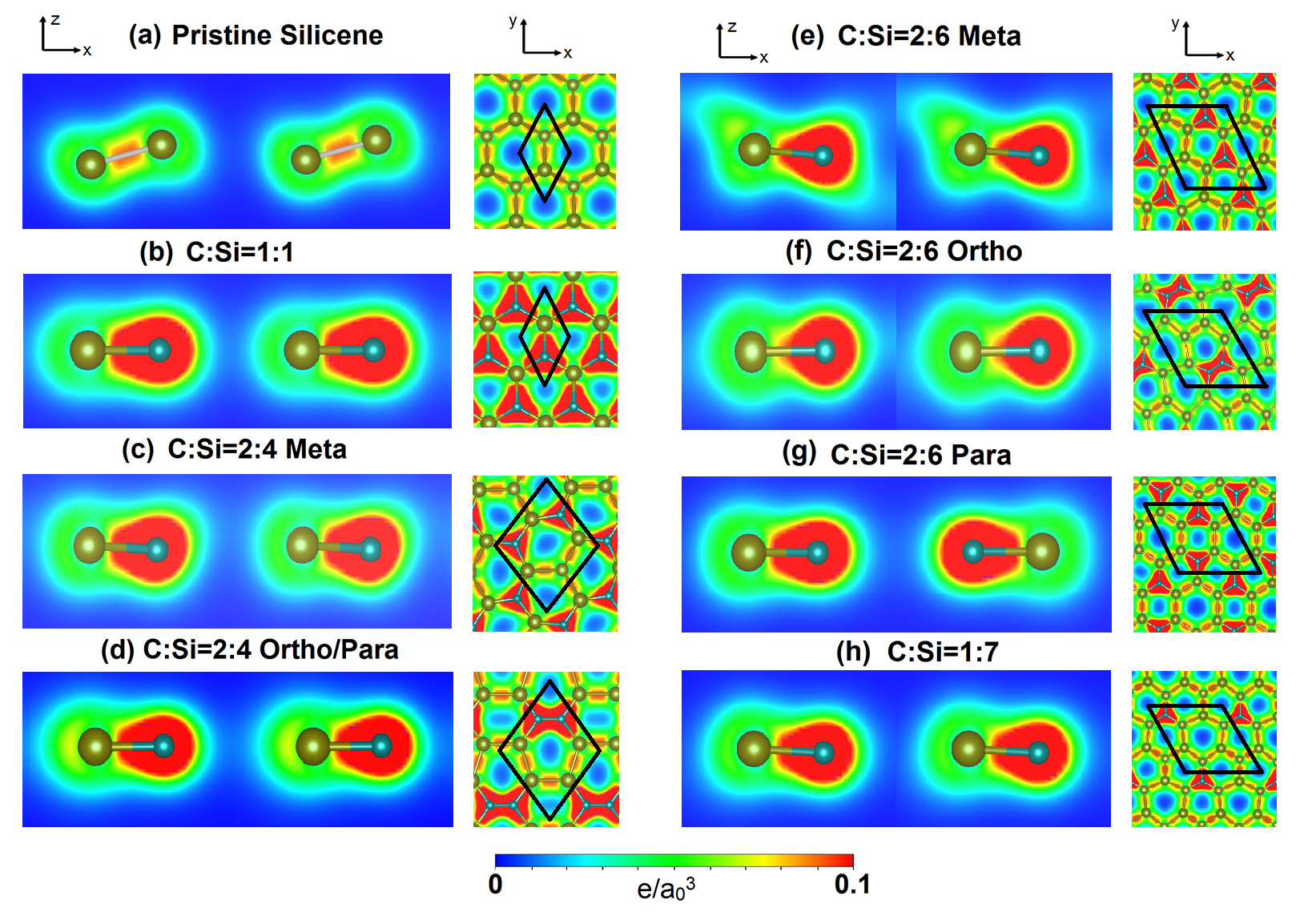
The spatial charge density distributions are able to provide certain observable evidences regarding the existence of the impure/pure and chemical bondings as well as their non-orthogonalities or orthogonalities. Pristine 2D silicene, as clearly displayed in Fig. 4(a) with the - and -plane projections, shows the well-defined - and - orbital hybridizations, especially for the latter. In our notation, is a symmetric distribution around the Si-Si bond center. Most of the charge density is accumulated between two silicon atoms [the red region], corresponding to the very strong bonding of three orbitals. The neighboring Si-atoms are also attracted together through the parallel orbitals perpendicular to the plane, in which the bonding appears in the outer region shown by the light green/blue color. As a result of buckling, they have the weak, but significant hybridizations under the non-orthogonality of and chemical bondings. When the Si-Si bonds become Si-C ones under full substitution, presents a dramatic transformation, being clearly illustrated in Fig. 4(b). The charge density is highly asymmetric with respect to the C-Si bond center, mainly owing to the different electron affinities of the guest and host atoms. There exist more carriers around the guest C-atoms [the red region]; that is, electrons are transferred from silicon to carbon atoms. The whole C-Si bonds consist of a planar honeycomb lattice with a stronger bonding, compared with those of a pristine one [Fig. 4(a)]. The and bondings could be roughly defined under the impure - and - orbital hybridizations, respectively. They are directly reflected in the - and -electronic valence subbands, with direct crossings [Fig. 3(b)]. Most important, two kinds of chemical bondings are orthogonal to each other. Therefore, the orbital hybridizations are negligible in the [1:1] case. Each Si-C bond has the identical chemical environment, i. e., only one chemical bond in a unit cell. This clearly illustrates that it is relatively easy to simulate the first-principles band structure using the tight-binding model [34].
When the carbon concentrations are decreased [Figs. 4(c) through 4(h)], the existence of and chemical bondings is relatively easily examined from the spatial charge densities. There exist C-Si, Si-Si and even C-C bonds, for which the last ones are stable under the specific ortho cases [Table 1]. The almost symmetric carrier distributions are clearly revealed between two silicon atoms for any concentration and configuration, in which they possess the lowest charge density among three kinds of chemical bonds. Similar phenomena appear for C-C bonds with the highest carrier densities, e.g., values in Figs. 4(d) and 4(f) at and ortho conditions, respectively. Roughly speaking, the spatial charge densities in different chemical bonds are not sensitive to changes in various carbon substitutions. These further illustrates that the and chemical bondings might be well separated from each other. Therefore, they could be roughly defined in the carbon-substituted silicene systems. As a result, the fundamental low-energy properties are expected to be dominated by the -electronic states due to the modified Dirac cone structures. On the other hand, the different chemical bonds lead to complex orbital hybridizations and thus contribute to the difficulties in obtaining suitable phenomelogical models. When the first principles electronic energy spectra along the high-symmetry paths are successfully simulated by the tight-binding model with the non-uniform and multi-/single-orbital hopping integrals [35], the diversified essential properties could be fully explored in the near-future, e.g., the rich and unique magnetic quantization phenomena [33], as predicted/observed in layered graphene systems [36].
0.4 Density-of-states
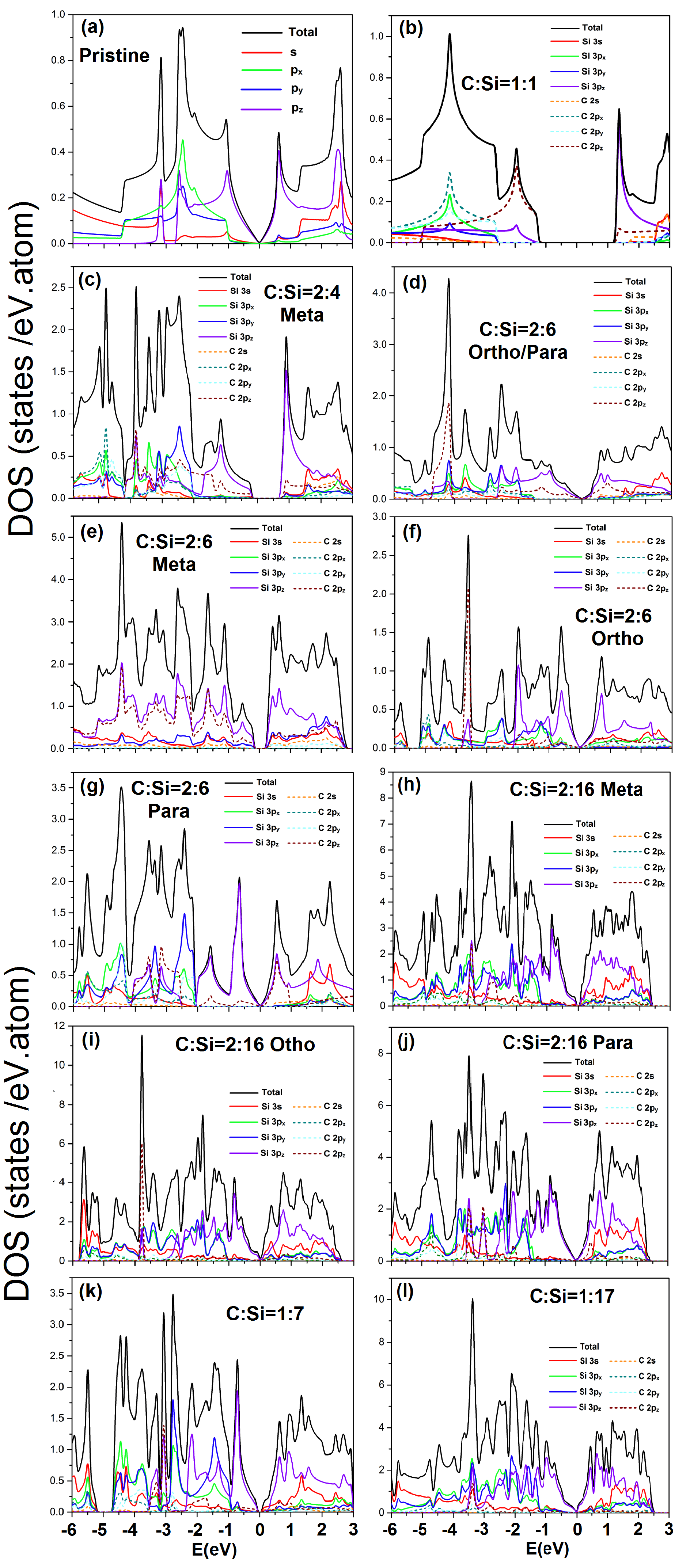
There are four/five categories of van Hove singularities in carbon-substituted silicene systems or pristine one, as clearly illustrated in Figs. 5(a) through 5(f). The orbital- and atom-decomposed density-of-states are very useful in fully understanding the bonding-induced special structures. The critical points, i.e., the band-edge states, in the energy-wave vector space include the linear Dirac cone structure, local minima or maxima of parabolic energy dispersion, saddle points, constant energy loops, which are closely related to band anticrossings, and partially flat bands [Figs. 3(a) through 3(l)]. Their densities-of-states generate the V-shape form, discontinuous shoulders, logarithmic divergent peaks, asymmetric peaks in the square root divergence, and delta-function-like peaks, respectively. A pure monolayer silicene in Fig. 5(a) displays an almost linear -dependence across the Fermi energy with a vanishing density-of-states [a quasi-V shape in the range meV meV; the purple curve of 3pz orbitals], a logarithmic symmetric -peak/-peak at 1.02 eV/0.59 eV, the [, ]-mixing created square root asymmetric peaks at [2.20 eV, 2.65 eV, 3.15 eV. The red, green and blue curves of (3px, 3px, 3py) orbitals], the -valley shoulder at 3.20 eV, the initial -[3px, 3py] shoulder at eV at the point, their M saddle point symmetric peak at eV and the K valley shoulder at eV. Consequently, the and bandwidths are 3.15 eV and 3.36 eV, respectively, It should be noted that the 3s orbitals [the red curve] are frequently accompanied by [3px, 3py] ones, but their contributions become significant at the deeper/higher energies, e.g., density-of-states within eV. The above mentioed features of van Hove singularities further illustrate the well behaved and chemical bondings and their weak, but important hybridization.
The structural features, energy and number of van Hove singularities exhibit a dramatic transformation under full carbon substitution, as indicated in Fig. 5(b). The special structures cover vanishing density-of-states within a band gap of eV at the K/K′ valley, the initial shoulder/delta function-like peak at 1.26 eV/1.26 eV [also shows the low-lying and bands in Fig. 3(b)], the 1.95 eV symmetric peak in the logarithmic divergence, the final shoulder at 5.00 eV, the first shoulder at 2.75 eV, the 4.10 eV logarithmic peak, and the second discontinuous structure at 7.01 eV. We also, observe that the first valence/conduction structure is dominated by the C-2pz orbitals/Si-3pz ones due to an obvious difference of ionization energy. The widths of the and first bands are 3.74 eV and 4.26 eV, respectively. Additionally, there is no evidence of - band mixing. This is mainly due to the absence of the simultaneous four-orbital structures. The fact that the sps bonding is absent agrees with the direct - subband crossings [Figs. 3(b)].
Within the whole energy range, the van Hove singularities become more complex during the decrease of guest-C-atom concentration, as a result of zone-folding effects as well as the significant [3s, 3px, 3py, 3pz]-[2s, 2px, 2py, 2pz] multi-orbital hybridizations. For example, the [2;4]-meta and [2:4]-ortho configurations, as clearly illustrated in Figs. 5(c) and 5(d), exhibit diverse low-energy van Hove singularities arising from the dominant 3pz-2pz chemical bonding. The former has a -electronic zero density-of-states in the 0.90 eV-gap region [the valley in Fig. 3(c)], a threshold valence shoulder at eV [the first composite conduction state structure due to the discontinuous shoulder and delta function-like peak at 0.45 eV], a strong logarithmic peak at eV, as well as the second and third step structures at eV and eV, respectively. Regarding the latter, the 3pz-2pz-diversified van Hove singularities show a gapless V-shape [a Dirac cone energy spectrum in Fig. 3(d)], the first valence shoulder at eV [the initial conduction shoulder at 0.30 eV], the logarithm-step composite structure at eV, the symmetric peak arising from two opposite shoulders at eV, a similar one at eV, and the -eV asymmetric peak in the square root form. The widths of the -band in the former and latter cases are estimated to be 4.05 eV and 4.70 eV, respectively. Furthermore, the first -bands are wider than 4.5 eV. Obviously, the low-energy physical phenomena are dominated by the 3pz orbitals of Si-host atoms.
As the guest-atom concentration is declined, there appear additional van Hove singularities. Overall, in this way, one is able to characterize the width of the -band from the effective distributions of the [3pz, 2pz] orbitals for any concentration and configuration [Figs. 5(a) through 5(l)]. However, the opposite is true for the first -band width except for full substitution and the pristine cases [Figs. 5(a) and 5(b)]. Certain van Hove singularities, close to the Fermi level, are very useful to comprehend the band-edge states in the first pair of the valence and conduction bands. The main features cover the vanishing density-of-states at/across the Fermi level [Figs. 5(c) through 5(e)]/[Figs. 5(d) through 5(g)], the electron-hole asymmetry near the first pair of clearly identifiable shoulders, the prominent peak in logarithmic form, the second and third shoulders and so on. Finally, the dip structure at , with a very small gap comparable to the broadening factor, will come to exist for a sufficiently low concentration, e.g., the almost gapless behavior in the [1:17] case [Fig. 5(l)]. We also noticed that the single-particle interactions of spin-orbital couplings cannot create any significant effects on the electronic properties and thus the other essential properties.
High-resolution scanning tunneling spectroscopy (STS) is an efficient method which could serve to identify the valence and conduction band-edge states [the van Hove singularities of the density-of-states. So far, they have confirmed the rich and unique density-of-states in dimension, stacking, layer number dependent graphene based materials, such as, the width and edge structure dominated/chirality and radius related band gaps and considerable asymmetric prominent peaks in 1D semiconducting graphene nanoribbons/carbon nanotubes [37]/[38], the V-shape structure with a dip at the Fermi level in monolayer graphene [39], the Dirac point red shift thorough alkali adatom chemisorption [-type doping] [40], the gate-voltage-created band gap in bilayer AB-stacked graphene [41], surface state peak just at in trilayer ABC stacked graphene [42], the semimetallic behavior [finite density-of-states at ] and the clearly symmetric and peaks at mid energies for Bernal graphite [43]. Similar STS examinations could be conducted on the various van Hove singularities in carbon-substituted silicene systems, covering the zero, finite gap semimetallic band properties, the and band widths, and the configuration as well as concentration dependent five types of special structures [V shape across the Fermi level, shoulders, symmetric peaks in the logarithmic form, delta function-like ones, i.e., square root asymmetric peaks in Figs. 5(a) through 5(l)]. Both experimental STS and ARPES results would provide sufficient information on the strength relations among the , and sp3 bondings during the chemical substitutions of guest atoms.
4. Concluding Remarks and Summary
Chemisorption and substitution of Si-guest atoms on monolayer graphene present unusual geometric properties, which are directly reflected in the spatial charge distributions. Si-adsorbed graphene is a non-buckled honeycomb lattice under optimal bridge-site positioning. A planar structure clearly indicates a very small variation in the bonding of C-[2s, 2px, 2py] orbitals. Therefore, they hardly take part in Si-C bonds. This adsorption configuration is similar to that of graphene oxide [44], but there is a slight buckling in the latter. The Si-C bond length is about 2.1-2.5 , leading to the significant multi-orbital hybridizations. Furthermore, the C-C bond lengths remain almost unchanged. According to the detailed analyses on the 3D charge density distributions, their spatial variations, as well as the atom and orbital projected density-of-states, the sp3-p multi-orbital hybridizations are deduced to determine the chemical Si-C bonds.
The theoretical predictions on the bridge site and Si-C/C-C bond lengths could be examined using high-resolution STM/TEM/LEED measurements. Also, Si-substituted graphene systems display planar geometries under multi-orbital chemical bondings in Si-C/C-C/Si-Si bonds. The Si-C bond length is about 1.62-1.83 , being shorter than those in the Si-adsorbed systems. This means that four orbitals in host and guest atoms are strongly hybridized with one another. The STM experiments are suitable for examining the predicted Si-C, C-C and Si-Si bond lengths. Any chemisorption and substitution of Si-guest atoms significantly modify the unusual band structure of monolayer graphene, especially the zero gap semiconducting behavior and linear Dirac cone due to the bondings of the 2pz orbitals. In the 100 double- and single-side adsorption cases, Si-adsorbed graphene systems are semimetals with free conduction electrons and valence holes. For the low concentration systems, they belong to the -type metals with only free valence holes. In general, the Dirac cone structure near the stable valley is seriously distorted after Si-chemisorption. There are more valence and conduction energy subbands, accompanied by the various band-edge states within an entire energy spectrum, e.g., the emergent low-lying energy bands along the K and M directions. However, the bands, which arises from the [2px, 2py] orbitals of carbon atoms, exhibit a robust red shift of 1 eV and 0.5 eV for 100 and lower-concentration cases, respectively.
The above mentioned important results directly reveal critical mechanisms, i.e., , the multi-orbital hybridizations of sp3-p in Si-C bonds, sp3-sp3 in Si-Si bonds, and sp2-sp2/ in C-C bonds. Such chemical bondings mainly produce four Si- and C-orbitals, as a result of the bridge-site adsorption positions, as well as the binding energies and charge distributions of the separated orbitals. High resolution ARPES measurements are very useful in verifying the low-lying valence bands near/crossing the Fermi level along K and M and the rigid bands initiated from the valley. On the other hand, all substitution results in semiconducting behavior with a finite or zero band gap. The Dirac cone structure presents a deviation from the point, a strong distortion, or even destruction. The number of valence and conduction energy subbands remains the same after chemical substitutions. Furthermore, they are co-dominated by the Si-guest and C-host atoms.
The main features of the band structure in Si-substituted graphene are dominated by the sp2-sp2 and p-p orbital hybridizations in Si-C/C-C/Si-Si bonds. Several unusual van Hove singularities in the atom and orbital decomposed density-of-states are created under the Si-guest-atom chemisorption and substitution. Pristine monolayer graphene only presents a V-shaped structure with a vanishing value at the Fermi level, the logarithmic symmetric -/-peaks at 2.41 eV/1.81 eV, and a shoulder structure at eV, in which the former two and the last one, respectively, correspond to the and bondings of carbon atoms. The strong -bonding evidence is totally destroyed by chemisorption except for the very diluted Si-adatoms. They are replaced by a finite density-of-states at , many shoulders, and peak structures. Furthermore, they are co-dominated by the four Si-[3s, 3px, 3py, 3pz] orbitals and the single C-2pz orbital, since their contributions are merged together. Specifically, the -band shoulder comes to exist at 4.21 eV, 4.11 eV or 3.5 eV, and the 0.5-1.0 the red shift is closely related to the distinct ionization energies of Si and C atoms. The above-mentioned significant features further support and illustrate the sp3-sp3 sp2-sp2 multi-orbital hybridizations in Si-C bonds and C-C bonds, respectively. Concerning the substitution cases, density-of-states is zero within a finite energy range centered at the Fermi level, except for few systems with deformed V-shaped structures at . All the C-substituted silicene systems are finite- or zero gap semiconductors. The special structures, which originate from Si-3pz and C-2pz orbitals, appear simultaneously. Also, a similar behavior is revealed in Si-[3px, 3py] and C-[2px, 2py] orbitals. These further illustrate the critical single- and multi-orbital hybridizations in Si-C bonds. The predicted van Hove singularities could be verified by the high-resolution STS experiments [45].
Acknowledgments
This work was financially supported by the Hierarchical Green-Energy Materials (Hi-GEM) Research Center, from The Featured Areas Research Center Program within the framework of the Higher Education Sprout Project by the Ministry of Education (MOE) and the Ministry of Science and Technology (MOST 108-3017-F-006 -003) in Taiwan.
References
- [1] Mauricio Terrones, Nicole Grobert , Humberto Terrones, Synthetic routes to nanoscale BxCyNz architectures, Carbon 40(10) (2002) 1665-1684.
- [2] Xingrui Deng, Hiroyuki Kousaka, Takayuki Tokoroyama, Noritsugu Umehara, Deposition and tribological behaviors of ternary BCN coatings at elevated temperatures, Surface Coatings Technology 259 (2014) 2-6.
- [3] Adithya Prakash, Kalpathy B Sundaram , D Andres Campiglia, Photoluminescence studies on BCN thin films synthesized by RF magnetron sputtering, Materials Letters 183 (2016) 355-358.
- [4] M Terrones, A M Benito, C Manteca-Diego, W K Hsu, O I Osman and J P Hare et al, Pyrolytically grown BxCyNz nanomaterials: nanofibres and nanotubes Chemical Physics Letters, 257 (1996) 576-582.
- [5] Kris J Erickson, Ashley L Gibb, Alexander Sinitskii, Michael Rousseas, Nasim Alem, James M Tour and Alex K Zettl 2011 Longitudinal Splitting of Boron Nitride Nanotubes for the Facile Synthesis of High Quality Boron Nitride Nanoribbons, Nano Lett. 11(8) (2011) 3221-3226.
- [6] Li Zhang, Zhi-Yi Zhang, Ru-Ping Liang, Ya-Hua Li, and Jian-Ding Qiu, Boron-Doped Graphene Quantum Dots for Selective Glucose Sensing Based on the ”Abnormal” Aggregation-Induced Photoluminescence Enhancement, Anal. Chem. 86(9) (2014) 4423-4430.
- [7] Maiyong Zhu and Guowang Diao, Review on the progress in synthesis and application of magnetic carbon nanocomposites, Nanoscale 3 (2011) 2748.
- [8] Li-Feng Chen, Xu-Dong Zhang, Hai-Wei Liang, Mingguang Kong, Qing-Fang Guan, Ping Chen et al, Synthesis of Nitrogen-Doped Porous Carbon Nanofibers as an Efficient Electrode Material for Supercapacitors, American Chemical Society 6(8) (2012) 7092-7102.
- [9] Sakineh Chabi, Hong Chang, Yongde Xia and Yanqiu Zhu, From graphene to silicon carbide: ultrathin silicon carbide flakes Nanotechnology 27(7) (2016) 075602.
- [10] Huaixiu Zheng and Walter Duley, First-principles study of edge chemical modifications in graphene nanodots, Phys. Rev. B 78 (2008) 045421.
- [11] D W Boukhvalov, A N Rudenko, D A Prishchenko, V G Mazurenkoc and M I Katsnelson, Chemical modifications and stability of phosphorene with impurities: a first principles study, Phys. Chem. Chem. Phys. 17 (2015) 15209.
- [12] E Bekaroglu, M Topsakal, S Cahangirov and S Ciraci, First-principles study of defects and adatoms in silicon carbide honeycomb structures, Physics Review B 81 (2010) 075433.
- [13] Ngoc Thanh Thuy Tran, Dipendra Dahal, Godfrey Gumbs, Ming-Fa Lin, Adatom doping-enriched geometric and electronic properties of pristine graphene: a method to modify the band gap, Struct Chem 28(5) (2017) 1311-1318.
- [14] Duy Khanh Nguyen, Ngoc Thanh Thuy Tran, Yu-Huang Chiu and Ming-Fa Lin, Concentration-Diversified Magnetic and Electronic Properties of Halogen-Adsorbed Silicene, Scientific Reports 9 (2017) 13746 .
- [15] Deepthi Jose And Ayan Datta, Structures and Chemical Properties of Silicene: Unlike Graphene, Acc. Chem. Res. 47(2) (2014) 593-602.
- [16] Ruitao Lv, Maria Cristina dos Santos, Claire Antonelli, Simin Feng, Kazunori Fujisawa, Ayse Berkdemir, Large-Area Si-Doped Graphene: Controllable Synthesis and Enhanced Molecular Sensing, Adv. Mater. 26(45) (2014) 7593-7599.
- [17] Lian Sun, Cheng Han, Nan Wu, Bing Wang, and Yingde Wang, High temperature gas sensing performances of silicon carbide nanosheets with an n-p conductivity transition, RSC Adv. 8 (2018) 13697-13707.
- [18] G Kresse G, J Furthmüller, Efficient iterative schemes for ab initio total-energy calculations using a plane-wave basis setller, Phys. Rev. B 54 (1996) 11169.
- [19] G Kresse, D Joubert, From ultrasoft pseudopotentials to the projector augmented-wave method Phys. Rev. B 59 (1999) 1758.
- [20] J P Perdew, K Burke, M Ernzerhof, Generalized gradient approximation made simple, Phys. Rev. Lett. 77 (1996) 3865.
- [21] P E Blöchl, Projector augmented-wave method Phys. Rev. B 50 (1994) 17953.
- [22] Cheng-Cheng Liu, Hua Jiang, and Yugui Yao, Low-energy effective Hamiltonian involving spin-orbit coupling in silicene and two-dimensional germanium and tin, Physical Review B 84 (2011) 195430.
- [23] Andrzej Badzian, Stability of Silicon Carbonitride Phases, J. Am. Ceram. Soc. 85(1) (2002) 16-20.
- [24] C Elias, P Valvin, T Pelini, A Summerfield, C J Mellor, T S Cheng et al, Direct band-gap crossover in epitaxial monolayer boron nitride, Nature Communications 10 (2019) 2639.
- [25] H Sahin and F M Peeters, Adsorption of alkali, alkaline-earth, and 3d transition metal atoms on silicene, Physical Review B 87 (2013) 085423.
- [26] P R Wallace, The Band Theory of Graphite, Physical Review 71 (1947) 622.
- [27] C P Chang, C L Lu, F L Shyu, R B Chen, Y C Huang, M F Lin, Magnetoelectronic properties of the AB-stacked graphite, Physical Review B 87 (2013) 085423.
- [28] C L Lu, C P Chang, Y C Huang , J H Ho, C C Hwang, M F Lin, Electronic Properties of AA- and ABC-Stacked Few-Layer Graphites, J. Phys. Soc. Jpn. 76 (2007) 024701.
- [29] C P Chang, C W Chiu, F L Shyu, R B Chen, M F Lin, Magnetoband structures of AB-stacked zigzag nanographite ribbons Physics Letters A Physics Letters A 306 (2002) 137-143.
- [30] S C Chen, T S Wang, C H Lee and M F Lin, Magneto-electronic properties of graphene nanoribbons in the spatially modulated electric field, Physics Letters A 372 (2008) 5999-6002.
- [31] W A Harrison and J Tersoff, Tight binding theory of heterojunction band lineups and interface dipoles, Journal of Vacuum Science Technology B 4 (1986) 1068.
- [32] Po-Hsin Shih, Thi-Nga Do, Godfrey Gumbs, Hai-Duong Pham and Ming-Fa Lin, Electric-field-diversified optical properties of bilayer silicene, Optics Letters 44(19) (2019) 4721-4724.
- [33] Po-Hsin Shih, Thi-Nga Do, Godfrey Gumbs, Danhong Huang, Hai-Duong Pham and Ming-Fa Lin, Rich Magnetic Quantization Phenomena in AA Bilayer Silicene, Scientific Reports 9 (2019) 14799 .
- [34] J C Slater and G F Koster, Simplified LCAO Method for the Periodic Potential Problem, Physical Review 94 (1954) 1498.
- [35] Yu-Huang Chiu, Jon-Hsu Ho, Yen-Hung Ho, Der-San Chuu, and Ming-Fa Lin, Effects of a Modulated Electric Field on the Optical Absorption Spectra in a Single-Layer Graphene, Journal of Nanoscience and Nanotechnology, 9(11) (2009) 6579-6586.
- [36] Thi-Nga Do, Chiun-Yan Lin, Yi-Ping Lin, Po-Hsin Shih, Ming-Fa Lin, Configuration-enriched magneto-electronic spectra of AAB-stacked trilayer graphene, Carbon 94 (2015) 619-632.
- [37] Duy Khanh Nguyen, Ngoc Thanh Thuy Tran, Thanh Tien Nguyen, Ming-Fa Lin, Diverse Electronic and Magnetic Properties of Chlorination-Related Graphene Nanoribbons, Scientific Reports 8 (2018) 17859.
- [38] Chiun-Yan Lin, Jhao-Ying Wu, Cheng-Pong Chang, Ming-Fa Lin, Magneto-optical selection rules of curved graphene nanoribbons and carbon nanotubes, Carbon 69 (2014) 151-161.
- [39] C W Chiu, S H Lee, S C Chen, and M F Lin, Electronic excitations in doped monolayer graphenes, Journal Of Applied Physics 106 (2009) 113711.
- [40] Minglei Sun, Wencheng Tang, Qingqiang Ren, Sake Wang, JinYu, Yanhui Du, Yajun Zhang 2015 First-principles study of the alkali earth metal atoms adsorption on graphene, Applied Surface Science 356 (2015) 668-673.
- [41] Chih-Wei Chiu, Yuan-Cheng Huang, Feng-Lin Shyu, and Ming-Fa Lin, Influence of anisotropic dipole matrix element on optical response of AB-stacked graphene superlattice, Optics letters 36(16) (2011) 3136-3138.
- [42] Chih-Wei Chiu, Yuan-Cheng Huang, Feng-Lin Shyu, and Ming-Fa Lin, Excitation spectra of ABC-stacked graphene superlattice Appl. Phys. Lett. 98 (2011) 261920.
- [43] Yen-Hung Ho, Yu-Huang Chiu, Wu-Pei Su, and Ming-Fa Lin, Magneto-absorption spectra of Bernal graphite, Appl. Phys. Lett. 99 (2011) 011914.
- [44] Xiaoxiao Chen, and Baoliang Chen, Macroscopic and Spectroscopic Investigations of the Adsorption of Nitroaromatic Compounds on Graphene Oxide, Reduced Graphene Oxide, and Graphene Nanosheets, Environ. Sci. Technol. 49 (2015) 6181-6189.
- [45] Guohong Li, A Luican, J M B Lopes dos Santos, A H Castro Neto, A Reina, J Kong and E Y Andrei, Observation of Van Hove singularities in twisted graphene layers, Nature Physics 6 (2010) 109-113.
Table Captions
Table 9.1: The optimal geometric structures of the carbon-substituted silicene systems under the various concentrations and configurations with the C-C, C-Si Si-Si bond lengths, the band gaps, the ground state energies per unit cell, and the height differences between A and B sublattices.