Decoupling superconductivity and correlated insulators in twisted bilayer graphene
Abstract
When bilayer graphene is rotationally faulted to an angle , theory predicts the formation of a flat electronic band and correlated insulating, superconducting, and ferromagnetic states have all been observed at partial band filling. The proximity of superconductivity to correlated insulators has suggested a close relationship between these states, reminiscent of the cuprates where superconductivity arises by doping a Mott insulator. Here, we show that superconductivity can appear without correlated insulating states. While both superconductivity and correlated insulating behavior are strongest near the flat band condition, superconductivity survives to larger detuning of the angle. Our observations are consistent with a “competing phases” picture, in which insulators and superconductivity arise from disparate mechanisms.
Strongly correlated electron systems often host dissimilar ground states vying closely for dominance. In certain instances, doping an interaction-driven phase can give rise to further correlated phases, in a hierarchy of emergence. Examples include the fractional quantum Hall phases that emerge doping the composite fermion sea in a partially filled Landau leveljain_composite_2007 and superconducting phases that arises upon doping a Mott insulator within Hubbard models thought to apply to the cuprateslee_doping_2006 . However, the complexity of correlated systems allows for other possibilities; namely, different interactions can simply compete, with the winner determined by experimental details controlled by doping and material structure. Disentangling the origin of different phases is often hampered by the closeness of the competition, which prevents targeted control of individual parameters in the effective Hamiltonian.
Twisted bilayer graphene (tBLG) offers an appealing platform to explore the interplay of competing states due to its high degree of tunability and panoply of apparently interaction driven ground states that break one or more system symmetriescao_correlated_2018 ; cao_unconventional_2018 ; yankowitz_tuning_2019 ; lu_superconductors_2019 ; sharpe_emergent_2019 ; serlin_intrinsic_2019 . The low energy band structure of tBLG consists of four spin- and valley-symmetry related copies of two low-energy bands within the reduced Brillouin zone created by the moire pattern; these two bands are themselves connected by gapless Dirac points in the absence of substrate or spontaneous breaking of lattice symmetriespo_origin_2018 ; carr_derivation_2019 ; koshino_maximally_2018 . Near a twist angle of , a resonant condition between interlayer twist angle and interlayer tunneling flattens these bands and isolates them from higher energy dispersive bandssuarez_morell_flat_2010 ; bistritzer_moire_2011 , rendering electronic interactions relevant in determining the ground state at finite filling of these bands. A central question has been the nature of the superconductivity, which in initial reportscao_unconventional_2018 ; yankowitz_tuning_2019 was found to appear only in close proximity to correlated insulators near half band filling, which we denote here (where indicates the number of charge carriers per moire superlattice unit cell, nm the moire period and the carrier density). Initial speculation suggested that the observed superconductivity might indeed be derived from the correlated insulators, as in the cuprates. However, the observation of superconducting behavior across much wider ranges of densitylu_superconductors_2019 —apparently filling the entire density range between correlated insulators at different integer —has suggested superconductivity as a competing phase, with the correlated insulators piercing an otherwise superconducting band. A recent workstepanov_interplay_2019 has suggested that insulating states can be selectively suppressed as compared to superconductivity by enhanced screening of interactions. However, the ubiquitous observation of correlated insulating states in most superconducting devices reported in the literature continues to fuel the speculation that these two disparate phenomena may be linked, or at least share a common origin.
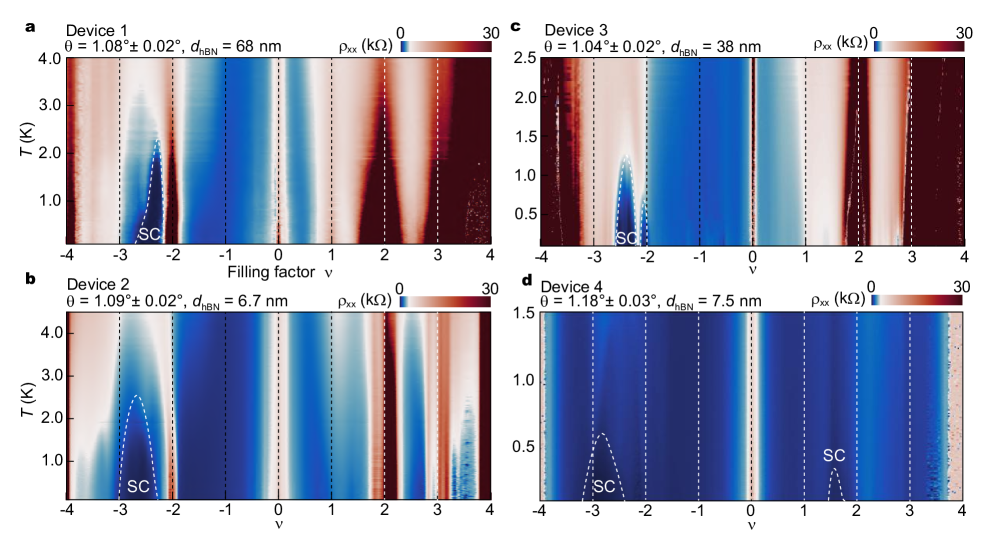
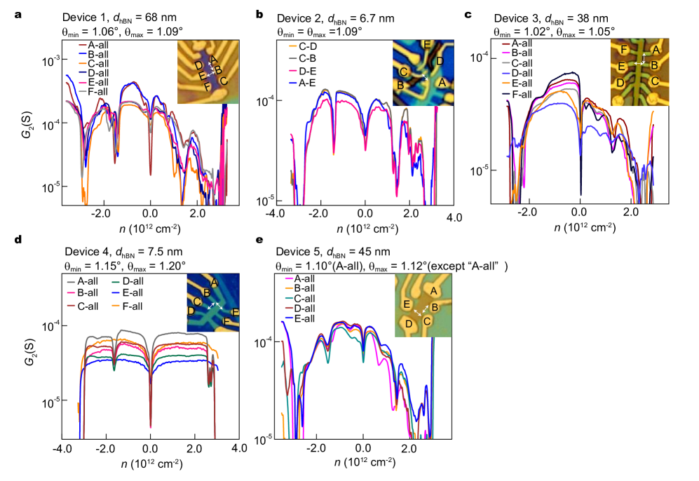
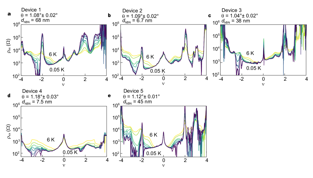
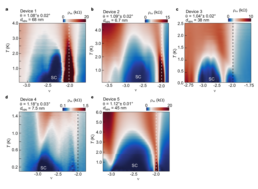
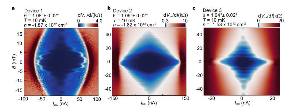
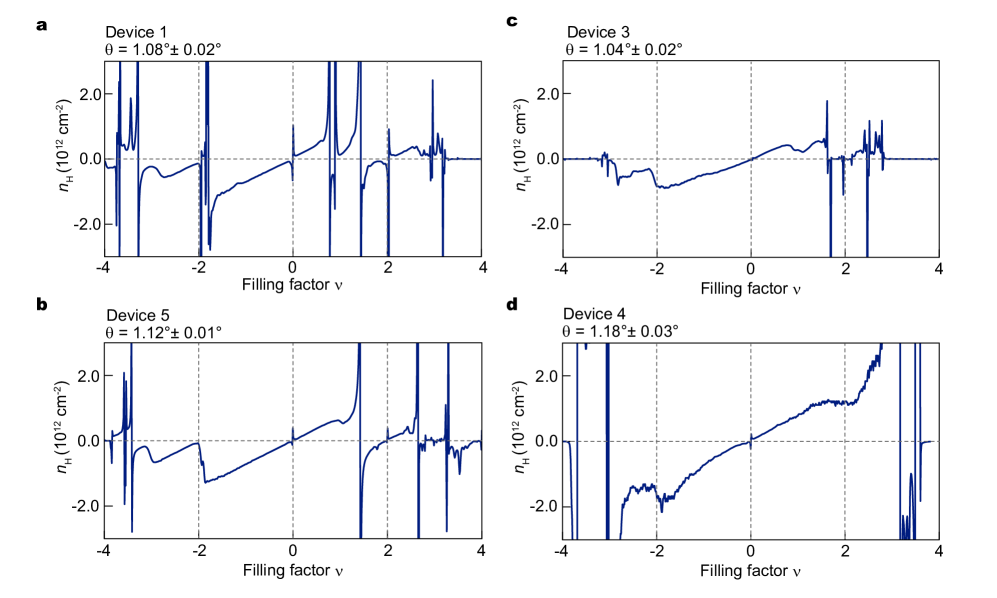
Here, we report superconducting behavior in tBLG devices decoupled from the appearance of correlated insulators, strongly suggesting disparate origins for the superconductivity and correlated insulating behavior. Figure 1 shows resistivity maps for four devices near the flat band condition as a function of temperature and carrier density with the later tuned across the entire range of the low energy bands, . All devices show robust signatures of superconductivity near (see also Figs. S4, S5 and S6), manifesting as a transition to a low-resistivity state at low temperatures, large non-linearity at low applied currents (a critical current), and phase coherent effects reminiscent of Fraunhoffer patterns in Josephson junctions. All tBLG devices used in this study are fabricated by a “cut-and-stack” technique (see Methods and Fig. S1 for details). In contrast to “tear-and-stack”kim_van_2016 ; cao_superlattice-induced_2016 , in which a monolayer is torn by an encapsulating hBN flake, we first cut the monolayer using an atomic force microscope (AFM)chen_evidence_2019 in order to prevent unintentional strain developing during the stacking process. This fabrication technique reproducibly leads to devices with twist angle inhomogeneity of on 10 m length scale, as quantified by two terminal conductance measurements across different contacts (Fig. S3). The devices further employ a bottom graphite or graphene gate to reduce charge inhomogeneityyankowitz_tuning_2019 ; lu_superconductors_2019 . Devices 1, 2 and 5 (shown in Figs. 1a, b and S5e, respectively) are closest to the flat band condition with , 1.09∘, and 1.12∘, respectively. All show superconductivity, correlated insulating states at , as well as additional insulating states or resistivity peaks at and consistent with previous observations in homogeneous tBLG under highyankowitz_tuning_2019 and ambient pressurelu_superconductors_2019 . In contrast, Devices 3 and 4, which are both farther from the flat band condition in angle at =1.04∘ and 1.18∘, respectively, show superconductivity despite the absence of an insulating state at (for Device 3) and total absence of any correlated insulating states at all (for Device 4).
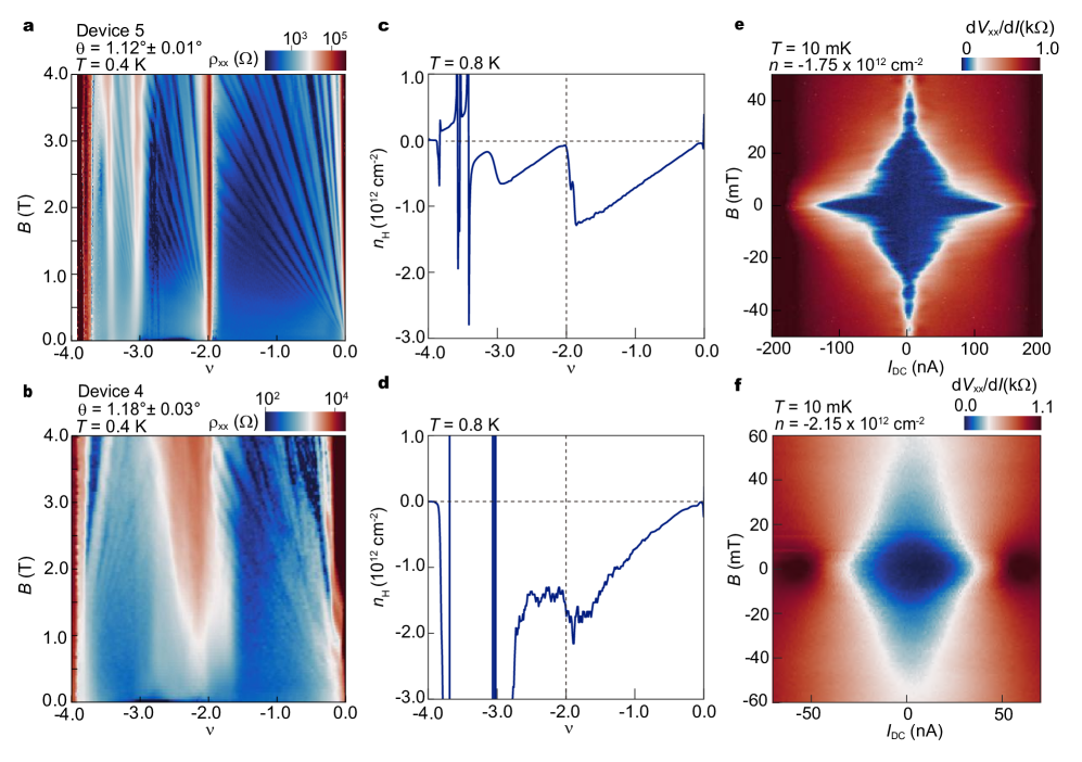
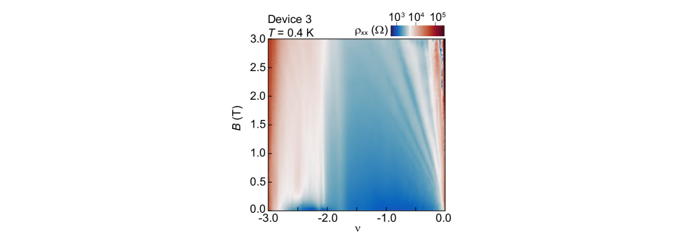
The contrasting behavior observed between Devices 1-2 and 3-4 raises the question of the role of disorder, particularly inhomogeneities in which may vary from sample to sample and obscure the intrinsic phenomenology of tBLG. For example, previous studies of twisted bilayer graphene have found that in the low temperature limit, superconductivity may obtain even at exactly cao_unconventional_2018 ; yankowitz_tuning_2019 , a finding attributed to percolation of superconducting domains due to variations in the local across the sample. The absence of an insulating state at in the devices presented here appears instead to be intrinsic, based on several observations. First, devices with and without a correlated insulator at show distinct behavior in finite magnetic field (Figs. 2a and b). Fig. 2a shows magnetoresistance of Device 5. A sequence of quantum oscillations, with an apparent degeneracy of 2, is clearly visible originating at , indicating the formation of a new Fermi surface associated with this insulating state. In contrast, for Devices 3 and 4 (Figs. 2b and S8), we observe no strong quantum oscillations originating from . In addition, the apparent resetting of the Hall density typically concomitant with the appearance of a correlated insulator at (Fig. 2c) as is observed in Device 5 (see also Figs. S11a and b), is suppressed in Device 3 (Fig. S11c) and nearly completely absence in Device 4 (Fig. 2d). In Device 4, shown in Fig. 2b, the neighborhood of shows only a strong magnetoresistance over a broad range of filling factor, devoid of oscillations but bracketed on either side by quantum oscillations originating from and . The distinct behavior of quantum oscillations and Hall effect in Devices 3 and 4 support the absence of significant interaction-induced Fermi surface reconstruction near in detuned devices as an intrinsic property.
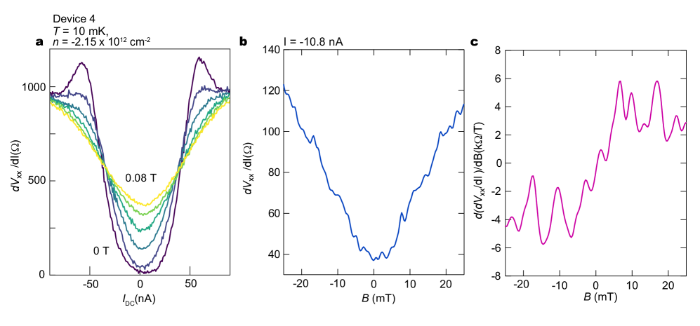
While the quantum oscillations show highly contrasting behavior between flat band and detuned devices, superconducting states appear to be phenomenologically similar to each other. Figures 2e and f show d/d versus magnetic field () and DC current () at 10 mK in Devices 5 and 4 at density of and cm-2, respectively; similar data for Devices 1, 2 and 3 is shown in Fig. S10. All devices show an apparent critical current, weakly modulated by the applied magnetic field. The period of the oscillations varies from around 38 mT (see Figs. 2e and S9), indicating an effective junction area of S 0.250.67 m2 , using S = , where = is the superconducting flux quantum, is Planck’s constant, and is the charge of the electron. In prior work, these Fraunhofer-like oscillations have been attributed to the presence of Josephson junctions consisting of small metallic or insulating domains within the devicecao_unconventional_2018 ; yankowitz_tuning_2019 ; lu_superconductors_2019 . Crucially, the Fraunhofer-like quantum interference pattern provides independent evidence of superconductivity beyond the vanishing low temperature resistance. This is critical for 2D superconductors, where the absence of detectable Meissner effect deprives experimentalists of the primary indicator of superconductivity in 3D materials. This is particularly important in high quality electronic systems such as graphene where ballistic transport can easily cause measured resistance to drop to zeromayorov_direct_2011 .
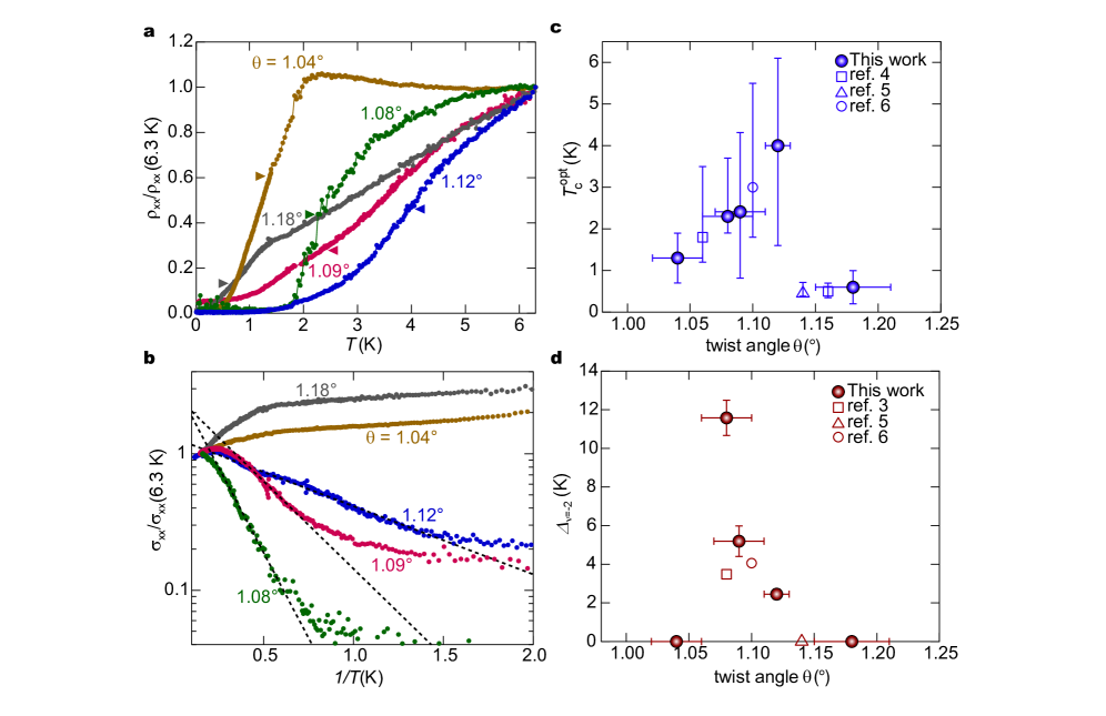
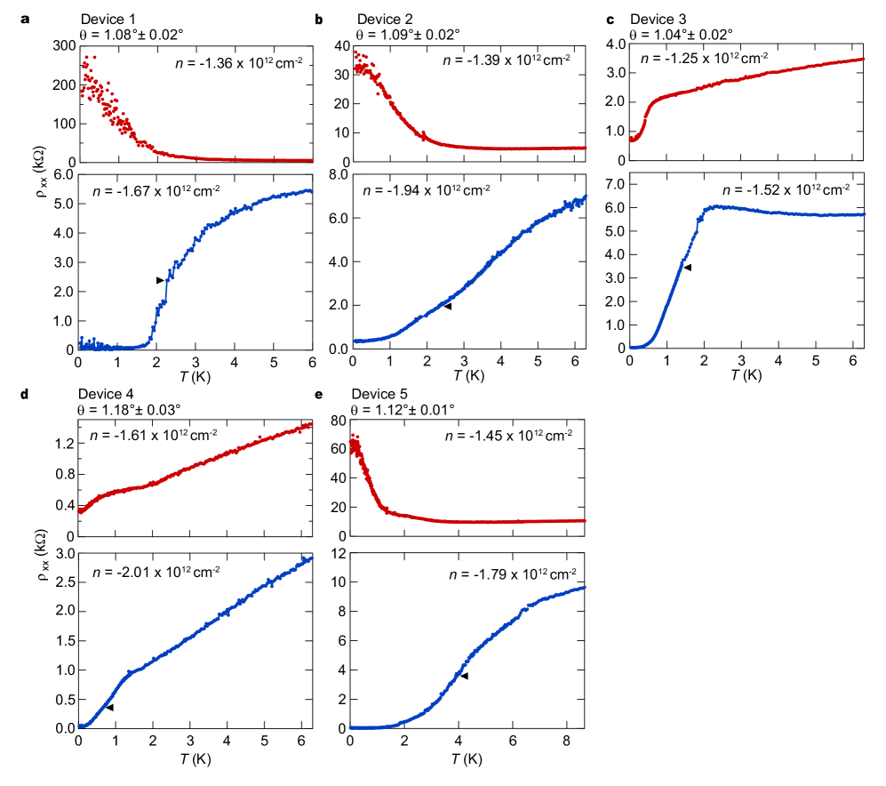
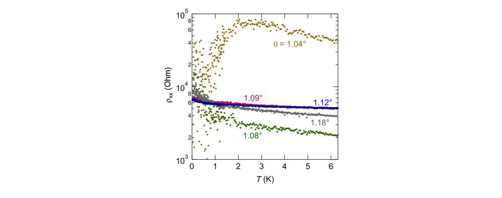
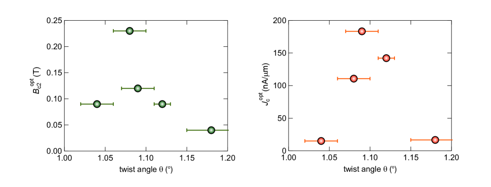
To quantitatively compare transport data across devices, Fig. 3a shows the temperature dependent resistance at the optimal doping for superconductivity normalized to the its value at 6.3 K, while Fig. 3b shows Arrhenius plots of the four terminal conductivity at . Most of the superconducting transitions show a broad characteristic as compared to other 2D superconductors yazdani_superconducting-insulating_1995 ; reyren_superconducting_2007 , complicating assignment of a critical temperature; we define as the temperature where is 50% of the normal state resistance, indicated by triangles in Fig. 3a. Devices 1, 2 and 5 show relatively high , comparable to the value reported in previous high-homogeneity 1.10∘ tBLGlu_superconductors_2019 . They also show activated behavior of the conductivity at , , allowing the gap to be determined from the experimental data. In Devices 3 and 4 ( and ), in contrast, there is no well-developed thermal activation gap at . Nevertheless, the devices show a clear superconducting transition, with a slightly lower than in the flat band devices. We summarize these observations in Figs. 3c and d. Both and trace out a dome-shaped behavior as a function of twist angle, reaching a maximum near 1.1∘. However, finite appears over a measurably narrower domain of as compared to the domain of finite .
Twisted bilayer graphene is a complex system in which the low temperature phase diagram is highly sensitive to a number of independent experimental parameters. As is evident in our data and consistent with theoretical modelingbistritzer_moire_2011 , the strength of interactions relative to bandwidth is highly dependent on twist angle, with detuning from 1.1∘ significantly reducing the role of interactions. Screening of electronic interactions may also play a rolegoodwin_critical_2019 . In particular, Devices 2 and 4 both feature graphite gates that are closer to the tBLG than the moire wavelength, which is expected to significantly screen Coulomb interactionsgoodwin_critical_2019 ; pizarro_internal_2019 as argued in a recent experimental study that also finds superconductivity without insulating states in tBLGstepanov_interplay_2019 . Disambiguating these effects precisely is complicated by the effect of twist angles between the tBLG layers and hBN encapsulants, as well as strain. Both of these effects (and presumably other, even more subtle sample details) are not controlled experimentally, and likely vary between devices. Unlike the twist angle or gate screening they are difficult quantify, and thus prevent carefully controlled experiments in which a single parameter is varied. The phase diagram of Figs. 3c-d thus represents only a coarse cut through the multidimensional parameter space governing tBLG physics.
Nevertheless, the observation of superconductivity in the absence of correlated insulating states constitutes powerful evidence that superconductivity arises independently. While more exotic scenarios cannot be ruled out definitively, a simple picture is that the superconductivity arises through the usual electron-phonon couplingwu_theory_2018 ; lian_twisted_2019 ; peltonen_mean-field_2018 ; angeli_valley_2019 . As a Fermi surface instability, superconductivity is sensitive to the density of states at the Fermi level rather than the total bandwidth. In contrast, the correlated insulating states are likely to break spin or valley symmetry, requiring a complete polarization of the band at an energy cost equivalent to the total bandwidth, as follows from a Stoner criterion. Correlated insulators thus become favored only when the bandwidth becomes exceptionally narrow, while superconductivity may be favored even far from the flat band condition, as the peak density of states remains high. Near 1.1∘, correlated insulators win the energetic competition at commensurate fillings, rearranging the electronic bands in the process and leading to the observation of superconductivity at diverse filling factors that vary from device to devicecao_unconventional_2018 ; yankowitz_tuning_2019 ; lu_superconductors_2019 . In this picture, tBLG resembles alkali-doped ramirez_superconductivity_2015 , in which BCS superconductivity or correlated insulator physics obtain at different dopings.
Methods
Device fabrication
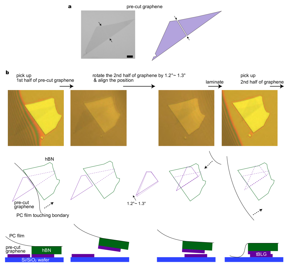
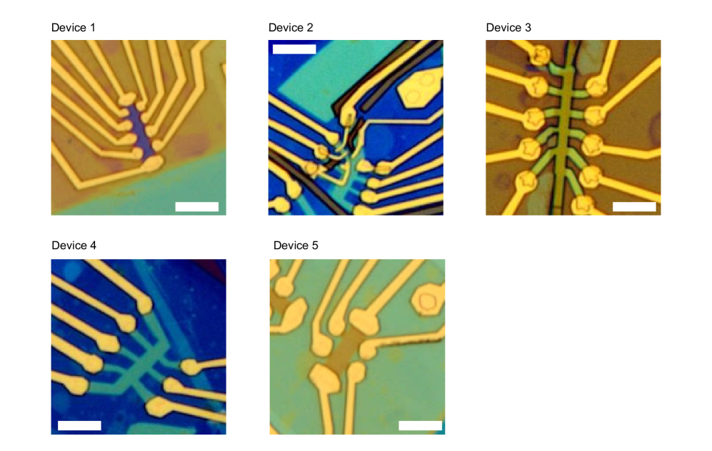
The tBLG used in this study were fabricated using a dry-transfer and “cut-and-stack” technique (Fig. S1) instead of the “tear-and-stack” techniquekim_van_2016 ; cao_superlattice-induced_2016 . Prior to stacking, we first cut graphene into two pieces using AFMchen_evidence_2019 (Fig. S1a) to prevent the unintentional strain in tearing graphene. We used a poly(bisphenol A carbonate) (PC)/polydimethylsiloxane (PDMS) stamp mounted on a glass slide to pick up a hBN flake (typically 3050 nm) at 90110∘C, and carefully pick up the 1st half of pre-cut graphene piece, rotate and pick up again the 2nd half of graphene piece in series at 25 ∘C using this hBN flake (Fig. S1b for details). Here we rotated graphene pieces manually by a twist angle of about 1.21.3∘. Finally, the 3-layer stack (hBN-tBLG) is transferred onto another stack for the bottom gate part (hBN-graphite or graphene gate), which is prepared in advance by the same dry transfer process and cleaned by the typical solvent wash using chloroform, acetone, methanol and IPA followed by vacuum annealing (400∘C for 8 hours) to remove the residue of PC film on the hBN surface. We did neither squeeze the bubbles nor perform any heat annealing after the stack is completed to prevent the relaxation of tBLG. We selected a bubble free region as a channel area to prevent inhomogeneity. Electrical connections to the tBLG were made by CHF3/O3 etching and deposition of the Cr/Pd/Au (2/15/180 nm) metal edge-contactswang_one-dimensional_2013 . Following this process, we got 5 superconducting tBLG devices (presented in this paper) of about 2025 stacks.
Transport measurements
All transport measurements in this study were carried out in a dilution refrigerator (Bluefors LD400) with a base temperature of 10 mK, which is equipped with a 14 T superconducting magnet and heavy RF and audio frequency filtering with a cutoff frequency of 10 kHz. The temperature dependent measurements were done by controlling the temperature using a heater mounted on a mixing chamber plate. Standard low frequency lock-in techniques with Stanford Research SR860 amplifiers were used to measure the resistance and with an excitation current of 12 nA at a frequency of 17.777 Hz.
Twist angle determination
The twist angle is determined from the values of charge carrier density at which the insulating states at are observed, following , where = 0.246 nm is the lattice constant of graphene. The values of are determined from the sequence of quantum oscillations in a magnetic field that project to or for devices.
Acknowledgments
We thanks M. Yankowitz and D.K. Efetov for discussions and D.K. Efetov for sharing unpublished experimental data. This work was primarily supported by the ARO under W911NF-17-1-0323. Y.S. acknowledges the support of the Elings Prize Fellowship. K.W. and T.T. acknowledge support from the Elemental Strategy Initiative conducted by the MEXT, Japan and the CREST(JPMJCR15F3), JST. A.F.Y. acknowledges the support of the David and Lucille Packard Foundation and the Alfred P. Sloan foundation.
Author Contributions
Y.S. and J.G. fabricated tBLG devices. Y.S. performed the measurements and analyzed the data. Y.S. and A.F.Y. wrote the manuscript. T.T. and K.W. grew the hBN crystals.
Competing interests
The authors declare no competing financial interests.
References
- [1] Jainendra K. Jain. Composite Fermions. Cambridge University Press, 2007.
- [2] Patrick A. Lee, Naoto Nagaosa, and Xiao-Gang Wen. Doping a Mott insulator: Physics of high-temperature superconductivity. Reviews of Modern Physics, 78(1):17–85, January 2006.
- [3] Yuan Cao, Valla Fatemi, Ahmet Demir, Shiang Fang, Spencer L. Tomarken, Jason Y. Luo, Javier D. Sanchez-Yamagishi, Kenji Watanabe, Takashi Taniguchi, Efthimios Kaxiras, Ray C. Ashoori, and Pablo Jarillo-Herrero. Correlated insulator behaviour at half-filling in magic-angle graphene superlattices. Nature, 556(7699):80–84, April 2018.
- [4] Yuan Cao, Valla Fatemi, Shiang Fang, Kenji Watanabe, Takashi Taniguchi, Efthimios Kaxiras, and Pablo Jarillo-Herrero. Unconventional superconductivity in magic-angle graphene superlattices. Nature, 556(7699):43–50, April 2018.
- [5] Matthew Yankowitz, Shaowen Chen, Hryhoriy Polshyn, Yuxuan Zhang, K. Watanabe, T. Taniguchi, David Graf, Andrea F. Young, and Cory R. Dean. Tuning superconductivity in twisted bilayer graphene. Science, 363(6431):1059–1064, March 2019.
- [6] Xiaobo Lu, Petr Stepanov, Wei Yang, Ming Xie, Mohammed Ali Aamir, Ipsita Das, Carles Urgell, Kenji Watanabe, Takashi Taniguchi, Guangyu Zhang, Adrian Bachtold, Allan H. MacDonald, and Dmitri K. Efetov. Superconductors, Orbital Magnets, and Correlated States in Magic Angle Bilayer Graphene. arXiv:1903.06513 [cond-mat], March 2019. arXiv: 1903.06513.
- [7] Aaron L. Sharpe, Eli J. Fox, Arthur W. Barnard, Joe Finney, Kenji Watanabe, Takashi Taniguchi, M. A. Kastner, and David Goldhaber-Gordon. Emergent ferromagnetism near three-quarters filling in twisted bilayer graphene. Science, 365(6453):605–608, August 2019.
- [8] M. Serlin, C. L. Tschirhart, H. Polshyn, Y. Zhang, J. Zhu, K. Watanabe, T. Taniguchi, L. Balents, and A. F. Young. Intrinsic quantized anomalous Hall effect in a moir\’e heterostructure. arXiv:1907.00261 [cond-mat], June 2019. arXiv: 1907.00261.
- [9] Hoi Chun Po, Liujun Zou, Ashvin Vishwanath, and T. Senthil. Origin of Mott Insulating Behavior and Superconductivity in Twisted Bilayer Graphene. Physical Review X, 8(3):031089, September 2018.
- [10] Stephen Carr, Shiang Fang, Hoi Chun Po, Ashvin Vishwanath, and Efthimios Kaxiras. Derivation of Wannier orbitals and minimal-basis tight-binding Hamiltonians for twisted bilayer graphene: First-principles approach. Physical Review Research, 1(3):033072, 2019.
- [11] Mikito Koshino, Noah F. Q. Yuan, Takashi Koretsune, Masayuki Ochi, Kazuhiko Kuroki, and Liang Fu. Maximally Localized Wannier Orbitals and the Extended Hubbard Model for Twisted Bilayer Graphene. Physical Review X, 8(3):031087, September 2018.
- [12] E. Suárez Morell, J. D. Correa, P. Vargas, M. Pacheco, and Z. Barticevic. Flat bands in slightly twisted bilayer graphene: Tight-binding calculations. Physical Review B, 82(12):121407, September 2010.
- [13] R. Bistritzer and A. H. MacDonald. Moiré butterflies in twisted bilayer graphene. Phys. Rev. B, 84(3), July 2011.
- [14] Petr Stepanov, Ipsita Das, Xiaobo Lu, Ali Fahimniya, Kenji Watanabe, Takashi Taniguchi, Frank H. L. Koppens, Johannes Lischner, Leonid Levitov, and Dmitri K. Efetov. The interplay of insulating and superconducting orders in magic-angle graphene bilayers. arXiv:1911.09198 [cond-mat], November 2019. arXiv: 1911.09198.
- [15] Kyounghwan Kim, Matthew Yankowitz, Babak Fallahazad, Sangwoo Kang, Hema C. P. Movva, Shengqiang Huang, Stefano Larentis, Chris M. Corbet, Takashi Taniguchi, Kenji Watanabe, Sanjay K. Banerjee, Brian J. LeRoy, and Emanuel Tutuc. van der Waals Heterostructures with High Accuracy Rotational Alignment. Nano Letters, 16(3):1989–1995, March 2016.
- [16] Y. Cao, J. Y. Luo, V. Fatemi, S. Fang, J. D. Sanchez-Yamagishi, K. Watanabe, T. Taniguchi, E. Kaxiras, and P. Jarillo-Herrero. Superlattice-Induced Insulating States and Valley-Protected Orbits in Twisted Bilayer Graphene. Physical Review Letters, 117(11):116804, September 2016.
- [17] Guorui Chen, Lili Jiang, Shuang Wu, Bosai Lyu, Hongyuan Li, Bheema Lingam Chittari, Kenji Watanabe, Takashi Taniguchi, Zhiwen Shi, Jeil Jung, Yuanbo Zhang, and Feng Wang. Evidence of a gate-tunable Mott insulator in a trilayer graphene moiré superlattice. Nature Physics, 15(3):237, March 2019.
- [18] A. S Mayorov, R. V Gorbachev, S. V Morozov, L. Britnell, R. Jalil, L. A Ponomarenko, K. S Novoselov, K. Watanabe, T. Taniguchi, and A. K Geim. Direct evidence for micron-scale ballistic transport in encapsulated graphene at room temperature. 1103.4510, March 2011.
- [19] Ali Yazdani and Aharon Kapitulnik. Superconducting-Insulating Transition in Two-Dimensional $\mathit{a}$-MoGe Thin Films. Physical Review Letters, 74(15):3037–3040, April 1995.
- [20] N. Reyren, S. Thiel, A. D. Caviglia, L. Fitting Kourkoutis, G. Hammerl, C. Richter, C. W. Schneider, T. Kopp, A.-S. Rüetschi, D. Jaccard, M. Gabay, D. A. Muller, J.-M. Triscone, and J. Mannhart. Superconducting Interfaces Between Insulating Oxides. Science, 317(5842):1196–1199, August 2007.
- [21] Zachary A. H. Goodwin, Valerio Vitale, Fabiano Corsetti, Dmitri K. Efetov, Arash A. Mostofi, and Johannes Lischner. Critical role of device geometry for the phase diagram of twisted bilayer graphene. arXiv:1911.08464 [cond-mat], November 2019. arXiv: 1911.08464.
- [22] J. M. Pizarro, M. Rösner, R. Thomale, R. Valentí, and T. O. Wehling. Internal screening and dielectric engineering in magic-angle twisted bilayer graphene. Physical Review B, 100(16):161102, October 2019.
- [23] Fengcheng Wu, A. H. MacDonald, and Ivar Martin. Theory of Phonon-Mediated Superconductivity in Twisted Bilayer Graphene. Physical Review Letters, 121(25):257001, December 2018.
- [24] Biao Lian, Zhijun Wang, and B Andrei Bernevig. Twisted bilayer graphene: A phonon-driven superconductor. Physical review letters, 122(25):257002, 2019.
- [25] Teemu J Peltonen, Risto Ojajärvi, and Tero T Heikkilä. Mean-field theory for superconductivity in twisted bilayer graphene. Physical Review B, 98(22):220504, 2018.
- [26] M. Angeli, E. Tosatti, and M. Fabrizio. Valley Jahn-Teller Effect in Twisted Bilayer Graphene. Physical Review X, 9(4):041010, October 2019.
- [27] Arthur P. Ramirez. Superconductivity in alkali-doped C60. Physica C: Superconductivity and its Applications, 514:166–172, July 2015.
- [28] L. Wang, I. Meric, P. Y. Huang, Q. Gao, Y. Gao, H. Tran, T. Taniguchi, K. Watanabe, L. M. Campos, D. A. Muller, J. Guo, P. Kim, J. Hone, K. L. Shepard, and C. R. Dean. One-Dimensional Electrical Contact to a Two-Dimensional Material. Science, 342(6158):614–617, November 2013.
Supplementary Materials for
Decoupling superconductivity and correlated insulators in twisted bilayer graphene
Yu Saito, Jingyuan Ge, Kenji Watanabe, Takashi Taniguchi and Andrea F. Young
Correspondence to: andrea@physics.ucsb.edu