Observation of the spin-orbit gap in bilayer graphene by
one-dimensional ballistic transport
Abstract
We report on measurements of quantized conductance in gate-defined quantum point contacts in bilayer graphene that allow the observation of subband splittings due to spin-orbit coupling. The size of this splitting can be tuned from 40 to 80 by the displacement field. We assign this gate-tunable subband-splitting to a gap induced by spin-orbit coupling of Kane-Mele type, enhanced by proximity effects due to the substrate. We show that this spin-orbit coupling gives rise to a complex pattern in low perpendicular magnetic fields, increasing the Zeeman splitting in one valley and suppressing it in the other one. In addition, we observe the existence of a spin polarized channel of 6 at high in-plane magnetic field and of signatures of interaction effects at the crossings of spin-split subbands of opposite spins at finite magnetic field.
Bilayer graphene (BLG) represents an interesting platform for mesoscopic transport and quantum devices. The possibility of tuning the low-energy electronic bands with a perpendicular electric field is unique to this material McCann and Koshino (2013), and allows to open a band gap Oostinga et al. (2007); Zhang et al. (2009), to modify band curvatures, and to change the topology of the Fermi surface Varlet et al. (2014). As all of this is controlled by external electrostatic gates, it is possible to implement soft-confined one-dimensional channels and quantum dots, where most of the BLG is gapped. Recent technological advancements – mostly based on the encapsulation of BLG in hexagonal boron nitride (hBN) and on the use of graphite gates – have enabled the observation of spin and valley states in BLG quantum dots Eich et al. (2018a); Banszerus et al. (2018); Eich et al. (2018b) and of quantized conductance in gate defined quantum point contacts (QPCs) Overweg et al. (2018a, b); Kraft et al. (2018); Lee et al. (2019). BLG is also interesting for spintronics applications Datta and Das (1990); Gmitra and Fabian (2017); Island et al. (2019) because of its weak hyperfine and spin-orbit interaction Yang et al. (2011); Ingla-Aynés et al. (2016); Leutenantsmeyer et al. (2018); Xu et al. (2018); Konschuh et al. (2012). Spin-orbit (SO) coupling is indeed expected to open a gap of only a few tens of eV in the low energy spectrum of graphene and BLG Kane and Mele (2005); Min et al. (2006); Huertas-Hernando et al. (2006); Yao et al. (2007); Konschuh et al. (2012). The presence of a SO gap in BLG has been confirmed by the spin lifetime anisotropy in diffusive spin transport Leutenantsmeyer et al. (2018); Xu et al. (2018). For monolayer graphene, the SO gap has been quantitatively extracted only recently from resonance microwave measurements, giving a value around eV Sichau et al. (2019).
Probing such small energy scales by transport is challenging, but becomes feasible when having comparable energy scales in the system, such as small subband spacings in QPCs. In addition, small spacings enable observing the crossings of spin-split subbands in parallel magnetic fields. In this Letter we show that by studying a wide QPC with low subband spacings (0.3–0.5 meV) and comparably large Zeeman energy we can observe the SO gap in BLG, appearing as a feature at due to the splitting of the first subband of the QPC at zero magnetic field. Studying the Zeeman splitting of the subbands as a function of an in-plane magnetic field, we are able to determine the energy scales associated to the system, including the splitting of the first subband at zero magnetic field. The latter ranges from 40 to 80 eV, showing a monotonic dependence on the displacement field. The associated gap can be understood in terms of a substrate-induced enhancement of SO coupling of Kane-Mele type Kane and Mele (2005). We show that this type of coupling gives rise to a characteristics spin-valley texture in low perpendicular magnetic field, increasing the Zeeman splitting in one of the valley and suppressing it in the other. The small energy scales of our device allow also realizing a regime of high spin-polarization, with six fully spin-down polarized modes at high in-plane magnetic fields. Furthermore, at the crossings of spin-split subbands of opposite spins we observe signatures of electron-electron (e-e) interaction at high magnetic fields.
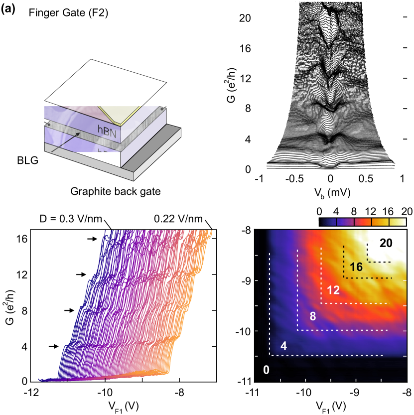
Our device is based on dry-transferred BLG, encapsulated in hBN and placed on a graphite back gate, see Fig. 1(a). We use the combination of two Cr/Au split gates (SG) and the graphite back gate (BG) to apply a perpendicular electric displacement field, , that opens up a band gap and depletes large parts of the BLG, defining a quasi-1D channel with a width of around 250 nm, connecting source and drain contacts. In addition, we place 200 nm wide finger gates across the channel to locally tune the Fermi energy and thus the number of open modes in the channel 111The finger gates are isolated from the side gates by a 25 nm thick Al2O3 layer.. This forms a QPC below each finger gate. An atomic force microscope image of the device is shown as inset in Fig. 1a.
We perform transport measurements in a He3/He4 dilution refrigerator at a temperature below 30 mK, using standard lock-in techniques. The four-terminal conductance as function of finger gate voltage 222Please note that here the finger gate F1 (F2) corresponds to FG2 (FG3) in Ref. Banszerus et al. (2018) features plateaus at 4, 8, 12 and for displacement fields ranging from 0.22 to 0.3 V/nm, see Fig. 1(b). The step-height indicates four-fold degeneracy (two-fold spin and two-fold valley) and near unity transmission through the QPC. Complete current pinch-off is observed for large -fields, i.e. large BLG band gaps. Reducing the displacement field increases the leakage current below the split gates, which leads in turn to an increase in the minimum conductance. Nevertheless, the height of the conductance steps remains nearly unaffected at . The near unity transmission through the QPC can be demonstrated more explicitly by using the second finger gate (F2), i.e. forming a second QPC placed 60 nm next to the first one, see Fig. 1(a). The conductance of the device as function of both gate voltages and shows steps of multiples of and depends only on the QPC with the lowest number of open modes, Fig. 1(d). This observation proves that the two QPCs have unity transmission and that the charge carriers travel ballistically through both QPCs, not thermalizing between them.
To estimate the subband spacings of the quasi-1D system we perform finite bias spectroscopy measurements. Fig. 1(c) depicts the four-terminal differential conductance through the QPC in units of as function of the DC bias voltage, , applied between the source and the drain contact (see Fig. 1(a)) for different at a fixed -field of 0.32 V/nm. The conductance traces bunch at multiples of for low bias voltages. At higher bias the plateaus smear out revealing energy spacings around 0.3 meV, 0.4 meV and 0.5 meV for the first three subbands (see Supplementary Material and below). These energies are a factor 10 smaller than what reported in Ref. Kraft et al. (2018), because of the large size of our device. Using a hard-wall confinement model for the lowest subband spacing, , where is the effective carrier mass in BLG ( is the electron mass), we estimate the width of the QPC to be nm. This value is in reasonable agreement with the lithographic channel width of 250 nm.
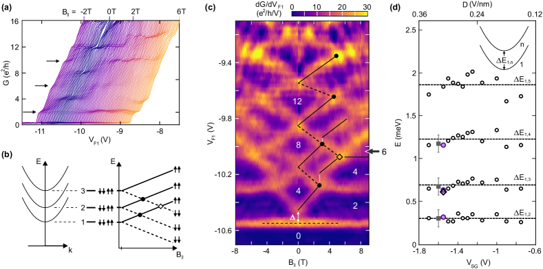
We investigate the spin structure of the subbands by studying the evolution of the conductance steps as function of an in-plane magnetic field, . In Fig. 2(a), the conductance is shown as a function of for fixed -fields ranging from to T. Plateaus at 2, 6, and 10 emerge with increasing magnetic field (see black arrows in Fig. 2(a)), indicating the lifting of the spin degeneracy of the subbands (see Fig. 2(b)). In Fig. 2(c), we plot the transconductance, d/d, as function of both and . The data reveal splittings of all subbands, as seen by the negative and positive slopes of spin-up and spin-down bands. Because of the small energy scales of our device, the Zeeman energy matches the subband spacing already for -fields between 2 and 4 T, resulting in the crossing of the spin-up bands with the spin-down bands of the next higher subband (crossings are marked by black dots in Figs. 2(c,b)). The feature independent of in Fig. 2(c) corresponds to the spin-down states of the first subband , which are locked to a finger-gate voltage slightly above V because of quantum capacitance effects. For T the spin-up states of the first subband cross the spin-down states of the third subband, giving rise to a regime with six fully spin-down polarized modes (; see black arrow in Fig. 2(c)) – a very high-polarization that makes such QPCs interesting for spin polarizers and detectors in ballistic spin transport devices Vila et al. (2019).
From the data of Fig. 2(c) we also determine the energy spacing between two neighboring subbands, . At the intersections of the spin-up and spin-down states of adjacent subbands, the Zeeman energy is equal to the spacing of the two subbands. Using the fact that in graphene and BLG the Lande factor is Tans et al. (1997); Lyon et al. (2017) (as confirmed by direct measurements on our device, see Supplementary Material), we determine the subband spacing at . The values determined in this way agree well with those extracted from finite bias measurements (compare gray squares and purple circles in Fig. 2(d)). The energy difference extracted from the position of the rotated square in Fig. 2(c) coincides with the sum , further confirming the consistency of the method.
We investigate the dependence of the subband spacing on the -field by performing measurements such as those shown in Fig. 2(c) but for different - configurations (see Supplementary Material). The subband spacings appear to be independent of the -field within the margin of the scattering of our data, see Fig. 2(d). This indicates (i) that the electronic width of the transport channel is not affected by the different stray-field contributions at different values, and (ii) that the BLG subband structure does not change appreciably when the band gap increases from to 35 meV 333The band gap depends on the displacement field approximately as 80 meV/(V/nm) Zhang et al. (2009).
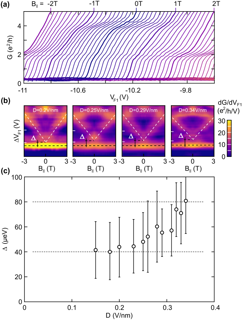
On energy scales below the subband spacing we find a pronounced splitting of the first subband at (marked by in Fig. 2(c)) leading to a plateau at , highlighted in Fig. 3(a) (a close-up of Fig. 2(a) around the first conductance step at low ). The feature, which is nearly unaffected by the in-plane magnetic field, can be well understood in terms of a splitting of the first subband caused by SO coupling of Kane-Mele type (see discussion below) Kane and Mele (2005); Min et al. (2006); Huertas-Hernando et al. (2006); Yao et al. (2007); Konschuh et al. (2012). Notably, we do not observe signatures of e-e interaction at low magnetic field, which should appear as a conductance step at at , whose height decreases with increasing magnetic field Tombros et al. (2011). The missing ”-anomaly” at low magnetic field can be explained by a suppression of the e-e interaction caused by the efficient screening of the graphite back gate Shapir et al. (2019) (which is only around nm away from the 250 nm wide transport channel), so that at low -field the SO coupling dominates over the interaction. We find an overall different situation at high magnetic fields ( T), where the SO coupling is quenched due to the magnetic field. We observe a discontinuous behaviour of the spin-up states at the Zeeman crossings (see jumps highlighted by white dashed lines in Fig. 2(c)), which indicates a spin-splitting caused by e-e interactions, known as the “0.7-analog” Graham et al. (2003); Berggren et al. (2005); Weidinger et al. (2018). This effect has been previously observed only in GaAs-based QPCs Graham et al. (2003).
The splitting of the first subband appears clearly in transconductance data such as those of Fig. 2(c) and Fig. 3(b). The analysis of the subband spacing performed before allows us to estimate the energy scale of the splitting of the lowest subband, , extracted from the transconductance data (see Supplementary Material). Performing this analysis for different values of the displacement field, we obtain values of that range from 40 to 80eV, with a monotonic dependence on the -field in the observed parameter range, see Fig. 3(c). This energy scale agrees well with what is expected for the SO gap in graphene and BLG Kane and Mele (2005); Min et al. (2006); Huertas-Hernando et al. (2006); Yao et al. (2007); Konschuh et al. (2012), and with the experimental value determined by Sichau et al. for graphene on SiO2 Sichau et al. (2019). The observed dependence of on the displacement field might originate from the fact that SO coupling in BLG is enhanced by proximity effects (i.e. by the overlap between the orbitals of graphene and of hBN) and from details of the -field dependent BLG band structure near the Fermi energy Gmitra and Fabian (2017); Zollner et al. (2019); Pri .
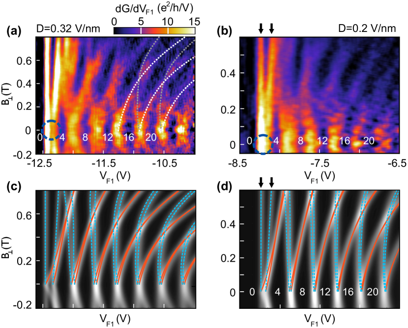
Figure 4(a,b) shows the transconductance as function of out-of-plane magnetic field, , and finger-gate voltage . In good agreement with earlier work Overweg et al. (2018b); Kraft et al. (2018), we observe the lifting of the valley degeneracy due to nontrivial valley-dependent orbital magnetic moments McCann and Fal’ko (2006) (see dashed lines in Fig. 4(a)), and a characteristic crossing pattern at increasing magnetic fields. The -field dependent splitting of the first subband at is also visible (see dashed circle in Fig. 4(a,b)). To reproduce most of this pattern – including the splitting of the first subband – we extended the single-particle model developed in Ref. Overweg et al. (2018b); Knothe and Fal’ko (2018) to take into account also the Zeeman term and the effects of SO coupling but neglecting e-e interaction. We write the SO coupling Hamiltonian as
where and refer to the layer, valley and spin degree of freedom, respectively. This Hamiltonian is of Kane-Mele (KM) type Kane and Mele (2005). Here we took into account that for BLG the valley and the layer degree of freedom are equivalent at low energies, and we also assume that the proximity-enhanced SO coupling coefficients are different in the upper (up) and lower (lo) layer of BLG.
Using an electrostatic simulation of the device to determine the local potential in the BLG (see Supplemental Material), we find overall good agreement between theory and experiment (compare Figs. 4(a,b) with 4(c,d)), by taking phenomenologically eV and eV in Fig. 4(c), and eV in Fig. 4(d). We thereby account for the effects that the -field localizes electrons on the upper layer, changes tight-binding hopping parameters, and effectively increases the proximity induced SO coupling. The calculations reproduce well the splittings of the first subband at zero and finite -field. Furthermore, the calculation reveal an interesting texture, where the spin-valley coupling due to at low -fields enhances the Zeeman splitting in one valley (diverging blue lines in Fig. 4(c,d)) but it suppresses the splitting in the other valley (converging red lines).
In summary, we have used the high energy-resolution provided by the confinement effect in a QPC to determine from transport measurements the energy gap due to SO coupling in BLG. The SO gap appears to be tunable between eV and eV. Controlling the SO coupling is interesting for spintronic applications such as spin-based field effect transistors and spin-orbit valves Datta and Das (1990); Gmitra and Fabian (2017); Island et al. (2019), and it might even allow to drive the system in the quantum spin-Hall phase and other interesting topological phases. Furthermore, our measurements in parallel magnetic field indicate the existence of a regime with six fully spin-down polarized modes, which indicates the potential of gate-defined QPCs as efficient spin polarizers and detectors in ballistic BLG devices.
Acknowledgements: We thank J. Fabian, M. Gmitra, A. Knothe, F. Haupt and B. van Wees for helpful discussions. This project has received funding from the European Union’s Horizon 2020 research and innovation programme under grant agreement No 785219 (Graphene Flagship), the Deutsche Forschungsgemeinschaft (DFG, German Research Foundation) under Germany’s Excellence Strategy - Cluster of Excellence Matter and Light for Quantum Computing (ML4Q) EXC 2004/1 - 390534769, through DFG (BE 2441/9-1 and STA 1146/11-1), the Austrian WWTF Project No. MA14-002, and by the Helmholtz Nano Facility Albrecht et al. (2017). Growth of hexagonal boron nitride crystals was supported by the Elemental Strategy Initiative conducted by the MEXT, Japan and the CREST(JPMJCR15F3), JST.
References
- McCann and Koshino (2013) E. McCann and M. Koshino, Rep. Prog. Phys. 76, 056503 (2013).
- Oostinga et al. (2007) J. B. Oostinga, H. B. Heersche, X. Liu, A. F. Morpurgo, and L. M. K. Vandersypen, Nat. Mater. 7, 151 (2007).
- Zhang et al. (2009) Y. Zhang, T.-T. Tang, C. Girit, Z. Hao, M. C. Martin, A. Zettl, M. F. Crommie, Y. R. Shen, and F. Wang, Nature 459, 820 (2009).
- Varlet et al. (2014) A. Varlet, D. Bischoff, P. Simonet, K. Watanabe, T. Taniguchi, T. Ihn, K. Ensslin, M. Mucha-Kruczyński, and V. I. Fal’ko, Phys. Rev. Lett. 113, 116602 (2014).
- Eich et al. (2018a) M. Eich, R. Pisoni, H. Overweg, A. Kurzmann, Y. Lee, P. Rickhaus, T. Ihn, K. Ensslin, F. Herman, M. Sigrist, K. Watanabe, and T. Taniguchi, Phys. Rev. X 8, 031023 (2018a).
- Banszerus et al. (2018) L. Banszerus, B. Frohn, A. Epping, D. Neumaier, K. Watanabe, T. Taniguchi, and C. Stampfer, Nano Lett. 18, 4785 (2018).
- Eich et al. (2018b) M. Eich, R. Pisoni, A. Pally, H. Overweg, A. Kurzmann, Y. Lee, P. Rickhaus, K. Watanabe, T. Taniguchi, K. Ensslin, and T. Ihn, Nano Lett. 18, 5042 (2018b).
- Overweg et al. (2018a) H. Overweg, H. Eggimann, X. Chen, S. Slizovskiy, M. Eich, R. Pisoni, Y. Lee, P. Rickhaus, K. Watanabe, T. Taniguchi, V. Fal’ko, T. Ihn, and K. Ensslin, Nano Lett. 18, 553 (2018a).
- Overweg et al. (2018b) H. Overweg, A. Knothe, T. Fabian, L. Linhart, P. Rickhaus, L. Wernli, K. Watanabe, T. Taniguchi, D. Sánchez, J. Burgdörfer, F. Libisch, V. I. Fal’ko, K. Ensslin, and T. Ihn, Phys. Rev. Lett. 121, 257702 (2018b).
- Kraft et al. (2018) R. Kraft, I. V. Krainov, V. Gall, A. P. Dmitriev, R. Krupke, I. V. Gornyi, and R. Danneau, Phys. Rev. Lett. 121, 257703 (2018).
- Lee et al. (2019) Y. Lee, A. Knothe, P. Rickhaus, H. Overweg, M. Eich, A. Kurzmann, T. Taniguchi, K. Wantanabe, V. Fal’ko, T. Ihn, and K. Ensslin, arXiv (2019), 1911.05968 .
- Datta and Das (1990) S. Datta and B. Das, Appl. Phys. Lett. 56, 665 (1990).
- Gmitra and Fabian (2017) M. Gmitra and J. Fabian, Phys. Rev. Lett. 119, 146401 (2017).
- Island et al. (2019) J. O. Island, X. Cui, C. Lewandowski, J. Y. Khoo, E. M. Spanton, H. Zhou, D. Rhodes, J. C. Hone, T. Taniguchi, K. Watanabe, L. S. Levitov, M. P. Zaletel, and A. F. Young, Nature 571, 85 (2019).
- Yang et al. (2011) T.-Y. Yang, J. Balakrishnan, F. Volmer, A. Avsar, M. Jaiswal, J. Samm, S. R. Ali, A. Pachoud, M. Zeng, M. Popinciuc, G. Güntherodt, B. Beschoten, and B. Özyilmaz, Phys. Rev. Lett. 107, 047206 (2011).
- Ingla-Aynés et al. (2016) J. Ingla-Aynés, R. J. Meijerink, and B. J. v. Wees, Nano Lett. 16, 4825 (2016).
- Leutenantsmeyer et al. (2018) J. C. Leutenantsmeyer, J. Ingla-Aynés, J. Fabian, and B. J. van Wees, Phys. Rev. Lett. 121, 127702 (2018).
- Xu et al. (2018) J. Xu, T. Zhu, Y. K. Luo, Y.-M. Lu, and R. K. Kawakami, Phys. Rev. Lett. 121, 127703 (2018).
- Konschuh et al. (2012) S. Konschuh, M. Gmitra, D. Kochan, and J. Fabian, Phys. Rev. B 85, 115423 (2012).
- Kane and Mele (2005) C. L. Kane and E. J. Mele, Phys. Rev. Lett. 95, 226801 (2005).
- Min et al. (2006) H. Min, J. E. Hill, N. A. Sinitsyn, B. R. Sahu, L. Kleinman, and A. H. MacDonald, Phys. Rev. B 74, 165310 (2006).
- Huertas-Hernando et al. (2006) D. Huertas-Hernando, F. Guinea, and A. Brataas, Phys. Rev. B 74, 155426 (2006).
- Yao et al. (2007) Y. Yao, F. Ye, X.-L. Qi, S.-C. Zhang, and Z. Fang, Phys. Rev. B 75, 041401(R) (2007).
- Sichau et al. (2019) J. Sichau, M. Prada, T. Anlauf, T. J. Lyon, B. Bosnjak, L. Tiemann, and R. H. Blick, Phys. Rev. Lett. 122, 046403 (2019).
- Note (1) The finger gates are isolated from the side gates by a 25\tmspace+.1667emnm thick Al2O3 layer.
- Note (2) Please note that here the finger gate F1 (F2) corresponds to FG2 (FG3) in Ref. Banszerus et al. (2018).
- Vila et al. (2019) M. Vila, J. H. Garcia, A. W. Cummings, S. R. Power, C. Groth, X. Waintal, and S. Roche, arXiv (2019), 1910.06194 .
- Tans et al. (1997) S. J. Tans, M. H. Devoret, H. Dai, A. Thess, R. E. Smalley, L. J. Geerligs, and C. Dekker, Nature 386, 474 (1997).
- Lyon et al. (2017) T. J. Lyon, J. Sichau, A. Dorn, A. Centeno, A. Pesquera, A. Zurutuza, and R. H. Blick, Phys. Rev. Lett. 119, 066802 (2017).
- Note (3) The band gap depends on the displacement field approximately as 80\tmspace+.1667emmeV/(V/nm) Zhang et al. (2009).
- Tombros et al. (2011) N. Tombros, A. Veligura, J. Junesch, M. H. D. Guimarães, I. J. Vera-Marun, H. T. Jonkman, and B. J. van Wees, Nat. Phys. 7, 697 (2011).
- Shapir et al. (2019) I. Shapir, A. Hamo, S. Pecker, C. P. Moca, Ö. Legeza, G. Zarand, and S. Ilani, Science 364, 870 (2019).
- Graham et al. (2003) A. C. Graham, K. J. Thomas, M. Pepper, N. R. Cooper, M. Y. Simmons, and D. A. Ritchie, Phys. Rev. Lett. 91, 136404 (2003).
- Berggren et al. (2005) K.-F. Berggren, P. Jaksch, and I. Yakimenko, Phys. Rev. B 71, 115303 (2005).
- Weidinger et al. (2018) L. Weidinger, C. Schmauder, D. H. Schimmel, and J. von Delft, Phys. Rev. B 98, 115112 (2018).
- Zollner et al. (2019) K. Zollner, M. Gmitra, and J. Fabian, Phys. Rev. B 99, 125151 (2019).
- (37) Private communication with J. Fabian and M. Gmitra .
- McCann and Fal’ko (2006) E. McCann and V. I. Fal’ko, Phys. Rev. Lett. 96, 086805 (2006).
- Knothe and Fal’ko (2018) A. Knothe and V. Fal’ko, Phys. Rev. B 98, 155435 (2018).
- Albrecht et al. (2017) W. Albrecht, J. Moers, and B. Hermanns, Journal of Large-Scale Research Facilities 3, 112 (2017).