Characterization and Analysis of On-Chip Microwave Passive Components at Cryogenic Temperatures
Abstract
This paper presents the characterization of microwave passive components, including metal-oxide-metal (MoM) capacitors, transformers, and resonators, at deep cryogenic temperature (4.2 K). The variations in capacitance, inductance and quality factor are explained in relation to the temperature dependence of the physical parameters and the resulting insights on modeling of passives at cryogenic temperatures are provided. Both characterization and modeling, reported for the first time down to 4.2 K, are essential in designing cryogenic CMOS radio-frequency integrated circuits, a promising candidate to build the electronic interface for scalable quantum computers.
Cryo-CMOS, quantum computing, cryogenic, capacitor, inductor, transformer, resonator, quality factor
1 Introduction
Complementary Metal Oxide Semiconductor (CMOS) circuits operating at cryogenic temperatures (Cryo-CMOS) have been proposed to build the scalable control electronics of quantum processors [1][2]. Besides that, Cryo-CMOS technology has been used in the past to fabricate cryogenic low noise amplifiers (LNAs) for high sensitivity receivers [3] and cryogenic LC oscillators for electron spin resonance detectors [4]. The advent of cryo-CMOS has triggered the need for the characterization of active and passive components at cryogenic temperatures as required to reliably predict the performance of cryogenic radio frequency integrated circuits (RFIC).
To some extent, this has been pursued by the scientific community in case of active devices, which is evident from papers that show DC characterization [5][6], RF and noise characterization [7], device mismatch [8][9], small signal and noise characterization [10] of CMOS devices in different technology nodes. Although inductors have been characterized over the military temperature range [11][12], we have characterized, for the first time, a wide set of passive components at cryogenic temperatures.
2 Test structures and measurement setup
Several test structures were fabricated in the 1P7M-4x1Z1U TSMC 40-nm CMOS with an ultra-thick metal layer to characterize the passive components at 4 K comprehensively.
A high-density metal-oxide-metal (MoM) capacitor was taped-out using stacked inter-digitated metal fingers in layers 1 to 5. For the inductance characterization, a multi-turn transformer was designed using the ultra-thick metal layer and avoiding substrate shielding, since high substrate resistivity is expected at 4 K thanks to carrier freeze-out. Finally, a resonator was designed to validate the cryogenic model of the inductor and capacitor.


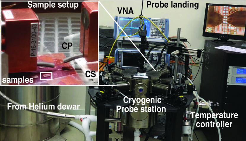
The measurements were done using ground-signal-ground (GSG) probes in a 40 GHz Lakeshore CPX cryogenic probe station with RS ZNB40 vector network analyzer (VNA) (see Fig.1). To ensure proper thermalization, the dies were mounted with a conductive glue on a copper plate (CP), which was securely taped to the sample holder. Due to the variation in the GSG probe electrical characteristics at cryogenic temperatures, short-open-load-through (SOLT) calibrations were done right before the measurement using a Picoprobe calibration substrate (CS) also mounted on the sample holder, at the measurement temperature.
3 Measurement, Analysis and Modelling
3.1 MoM capacitor
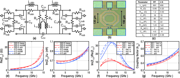
The MoM capacitor can be modeled as a -network [13] as shown in Fig.2 (a), where C is the actual capacitance due to the interdigitated metal fingers across an extra low-k inter-metal dielectric [14], and C represents the parasitic between the lowest metal layer and the ground plane (poly shield to filter substrate noise). R and L represent the equivalent series resistance and inductance respectively, of the traces and vias from the pad to the device terminals. The frequency dependent losses is modeled as R and L due to skin effect and R and L due to the dielectric. Note that the quality factor of the capacitor above 10 MHz is limited by the series resistance [15] and hence, the leakage resistance (modeled as a very high resistance across the capacitor terminals at DC) due to the interface traps [16] is ignored in the model.
Fig. 3 (a) shows the measured ( is the angular frequency), from which the C can be extracted at the lowest measured frequency (i.e., 100 MHz), where the effect of parasitic inductance is negligible [17]. Similarly, C can be extracted from measured . Both the capacitances incur slight change at 4 K compared to room temperature (RT) due to variation in the dielectric constant [18], as the thermal contraction of metals is negligible [19].
The measurement uncertainty increases when the desired impedance is negligible compared to the VNA reference impedance of 50 . Hence, at the frequencies below 5 GHz, the error in the determination of the series resistance and capacitor’s quality factor would be significant and is excluded in Fig. 3 (b). Due to reduction of dielectric and metal loss at lower temperatures, there is a boost in the quality factor at frequencies below 10 GHz. However, the dielectric loss does not improve over temperature above a certain frequency [15]. Consequently, a negligible quality factor improvement is observed above 15 GHz, when the dielectric loss is dominant, as can be gathered from Fig. 3 (b) and (c). Table I (Fig. 3 (d)) concludes the discussion on MoM capacitors and summarizes the change of the model parameters over temperature.
3.2 Transformer

The transformer can be modeled using the well-known frequency independent lumped model for on-chip spiral inductors [20] as depicted in Fig. 4 (a), where L and L represent the inductance, R and R describe the DC ohmic loss, of the primary and secondary windings, respectively. k represents the coupling factor of the transformer. C models the interwinding capacitance, C denotes the oxide capacitance, while C represents the capacitance due to metal lines running in parallel in the multi-turn primary winding. C and R model the substrate capacitance and resistance respectively.
R (extracted from shown in Fig. 4 (d) at 1 GHz where the skin effect is negligible) is 5 lower at 4 K compared to RT, due to the increase in copper conductivity () [19]. At higher frequencies, the skin effect dominates and the loss becomes proportional to , in which the skin depth , where and represent the magnetic permeability and conductivity of the conductor. Since the conductivity increases by 5, skin depth and thus the inductor loss at higher frequencies decreases by [21], as confirmed by Fig. 4 (d) for frequencies above 10 GHz. Furthermore, the increase in conductivity leads to a reduction in inductance by 5 [22], also confirmed by the measured winding’s inductance (extracted from at the lowest measured frequency) as shown in Fig. 4 (e).
Fig. 4 (f) reveals that the inductor peak quality factor (extracted from ) increases by 2.7 from RT to 4 K. The improvement is partially contributed (1.6 as verified from EM simulation) by the increase in conductivity and partly due to the reduction of tangential electric field losses in the silicon substrate, as it becomes highly resistive due to freeze-out.
Figure 4 (g) shows the measured k, calculated as , at both RT and 4 K. The coupling factor is mainly set by the physical dimensions of the transformer, which barely change over temperature (i.e., as shown in [19]). The slight increase in coupling factor at 4 K is due to the change in capacitive coupling caused by the change in dielectric constant as mentioned earlier.
Table II (Fig. 4 (c)) summarizes the values of model parameters at RT and 4 K. All the capacitors slightly change over temperature, which is also in line with the extracted MoM model. However, (R) and substrate coupling resistance (R) increases by 3 orders of magnitude at 4 K mainly due to substrate freeze out [23]. For low resistive substrates, the capacitance from the windings to the ground plane is dominated by C [24, 25], while for highly resistive substrates, the effective capacitance is lowered by C in series with C, resulting in a slight increase in the frequency where peak quality factor occurs. The self-resonance frequency of the transformer increases by 5, due to the decrease in both inductance and overlap capacitance. Furthermore, as can be gathered from Fig. 4 (d)-(g), EM simulations confirm all abovementioned behaviors and accurately predict the performance at 4 K; by increasing the copper conductivity by 5 and increasing the substrate resistivity by 1000, in the foundry metal stack.
4 Impact on RFICs
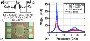
To analyze the impact of the cryogenic operation on RFICs like oscillators [26] and LNAs/PAs [27], a transformer-based resonator (matching network), shown in Fig. 5 (a) was designed. Its performance was estimated using the developed models and compared with measurement results. Fig. 5 (c) shows the input impedance of the resonator with Port2 open (), which determines an oscillator’s power consumption in a transformer based oscillator[26]. There is an increase in the impedance peak of the resonator, from RT to 4 K, due to the overall increase in quality factor, which is well predicted by the cryogenic model. Hence, one can obtain the same output voltage swing for half the current consumption, thus improving the oscillator’s power efficiency. The reduction in inductance and the effective parasitic capacitance causes the resonance to shift towards higher frequencies by 8 . The ratio of the resonant frequencies merely depends on the coupling factor, which increases by 4 as predicted by the model.

5 Conclusion
Passive components at cryogenic temperatures show in general higher quality factor (2) due to higher metal conductivity and lower loss in the substrate. However, the value of inductive and capacitive on-chip components slightly changes (i.e., 5) from RT to 4 K. Those variations can be replicated in an EM simulation by manipulating the resistivity of metals and substrate. As a result, RFIC designers can predict the performance of cryogenic passive devices both by using EM simulation and/or by scaling the presented lumped model parameters. This enables, in combination with existing Cryo-CMOS models, the reliable design of cryogenic RFIC needed for future large-scale quantum computers.
13
References
- [1] B. Patra, R. M. Incandela, J. P. G. van Dijk, H. A. R. Homulle, L. Song, M. Shahmohammadi, R. B. Staszewski, A. Vladimirescu, M. Babaie, F. Sebastiano, and E. Charbon, “Cryo-CMOS circuits and systems for quantum computing applications,” IEEE Journal of Solid-State Circuits, vol. 53, no. 1, pp. 309–321, Jan 2018, doi: 10.1109/JSSC.2017.2737549.
- [2] J. P. van Dijk, E. Kawakami, R. N. Schouten, M. Veldhorst, L. M. Vandersypen, M. Babaie, E. Charbon, and F. Sebastiano, “The impact of classical control electronics on qubit fidelity,” arXiv preprint arXiv:1803.06176, Mar 2018.
- [3] J. Schleeh, G. Alestig, J. Halonen, A. Malmros, B. Nilsson, P. A. Nilsson, J. P. Starski, N. Wadefalk, H. Zirath, and J. Grahn, “Ultralow-power cryogenic InP HEMT with minimum noise temperature of 1 K at 6 GHz,” IEEE Electron Device Letters, vol. 33, no. 5, pp. 664–666, May 2012, doi: 10.1109/LED.2012.2187422.
- [4] G. Gualco, J. Anders, A. Sienkiewicz, S. Alberti, L. Forró, and G. Boero, “Cryogenic single-chip electron spin resonance detector,” Journal of Magnetic Resonance, vol. 247, pp. 96 – 103, October 2014, doi: "10.1016/j.jmr.2014.08.013".
- [5] R. M. Incandela, L. Song, H. Homulle, E. Charbon, A. Vladimirescu, and F. Sebastiano, “Characterization and compact modeling of nanometer CMOS transistors at deep-cryogenic temperatures,” IEEE Journal of the Electron Devices Society, vol. 6, pp. 996–1006, April 2018, doi: 10.1109/JEDS.2018.2821763.
- [6] A. Beckers, F. Jazaeri, A. Ruffino, C. Bruschini, A. Baschirotto, and C. Enz, “Cryogenic characterization of 28 nm bulk CMOS technology for quantum computing,” in 2017 47th European Solid-State Device Research Conference (ESSDERC), Sept 2017, pp. 62–65, doi: 10.1109/ESSDERC.2017.8066592.
- [7] A. Siligaris, G. Pailloncy, S. Delcourt, R. Valentin, S. Lepilliet, F. Danneville, D. Gloria, and G. Dambrine, “High-frequency and noise performances of 65-nm MOSFET at liquid nitrogen temperature,” IEEE Transactions on Electron Devices, vol. 53, no. 8, pp. 1902–1908, Aug 2006, doi: 10.1109/TED.2006.877872.
- [8] N. C. Dao, A. E. Kass, C. T. Jin, and P. H. W. Leong, “Impact of series resistance on bulk CMOS current matching over the 5-300 K temperature range,” IEEE Electron Device Letters, vol. 38, no. 7, pp. 847–850, July 2017, doi: 10.1109/LED.2017.2709545.
- [9] P. A. ’t Hart, J. P. G. van Dijk, M. Babaie, E. Charbon, A. Vladimircscu, and F. Sebastiano, “Characterization and model validation of mismatch in nanometer CMOS at cryogenic temperatures,” in 2018 48th European Solid-State Device Research Conference (ESSDERC), Sep. 2018, pp. 246–249, doi: 10.1109/ESSDERC.2018.8486859.
- [10] A. H. Coskun and J. C. Bardin, “Cryogenic small-signal and noise performance of 32nm SOI CMOS,” in 2014 IEEE MTT-S International Microwave Symposium (IMS2014), June 2014, pp. 1–4, doi: 10.1109/MWSYM.2014.6848614.
- [11] R. Groves, D. L. Harame, and D. Jadus, “Temperature dependence of Q and inductance in spiral inductors fabricated in a silicon-germanium/BiCMOS technology,” IEEE Journal of Solid-State Circuits, vol. 32, no. 9, pp. 1455–1459, Sept 1997, doi: 10.1109/4.628763.
- [12] H. . Chiu, Y. . Lin, K. Liu, and S. . Lu, “Temperature and substrate effects in monolithic RF inductors on silicon with 6-m-thick top metal for RFIC applications,” IEEE Transactions on Semiconductor Manufacturing, vol. 19, no. 3, pp. 316–330, Aug 2006, doi: 10.1109/TSM.2006.879416.
- [13] K. Lee, S. Mohammadi, P. K. Bhattacharya, and L. P. B. Katehi, “Compact models based on transmission-line concept for integrated capacitors and inductors,” IEEE Transactions on Microwave Theory and Techniques, vol. 54, no. 12, pp. 4141–4148, Dec 2006, doi: 10.1109/TMTT.2006.886157.
- [14] F.-W. Tsai, K.-C. Wang, K.-C. Lin, C.-L. Lin, and S.-M. Jeng, “Extreme low-K dielectric film scheme for advanced interconnects,” U.S. Patent 7 626 245, Dec., 2009.
- [15] P. Riess and P. Baumgartner, “Temperature dependent dielectric absorption of MIM capacitors: RF characterization and modeling,” in 2006 European Solid-State Device Research Conference, Sep. 2006, pp. 459–462, doi: 10.1109/ESSDER.2006.307737.
- [16] V. F. Tseng and H. Xie, “Increased multilayer fabrication and RF characterization of a high-density stacked MIM capacitor based on selective etching,” IEEE Transactions on Electron Devices, vol. 61, no. 7, pp. 2302–2308, July 2014, doi: 10.1109/TED.2014.2325491.
- [17] H. Samavati, A. Hajimiri, A. R. Shahani, G. N. Nasserbakht, and T. H. Lee, “Fractal capacitors,” IEEE Journal of Solid-State Circuits, vol. 33, no. 12, pp. 2035–2041, Dec 1998, doi: 10.1109/4.735545.
- [18] F. A. Miranda, W. L. Gordon, V. O. Heinen, B. T. Ebihara, and K. B. Bhasin, Measurements of Complex Permittivity of Microwave Substrates in the 20 to 300 K Temperature Range from 26.5 to 40.0 GHz. Boston, MA: Springer US, 1990, pp. 1593–1599, doi: "10.1007/978-1-4613-0639-9-188".
- [19] P. Duthil, “Material Properties at Low Temperature,” pp. 77–95. 18 p, Jan 2015, doi: 10.5170/CERN-2014-005.77.
- [20] Y. Cao, R. A. Groves, X. Huang, N. D. Zamdmer, J. . Plouchart, R. A. Wachnik, T.-J. King, and C. Hu, “Frequency-independent equivalent-circuit model for on-chip spiral inductors,” IEEE Journal of Solid-State Circuits, vol. 38, no. 3, pp. 419–426, March 2003, doi: 10.1109/JSSC.2002.808285.
- [21] C. P. Yue and S. S. Wong, “Physical modeling of spiral inductors on silicon,” IEEE Transactions on Electron Devices, vol. 47, no. 3, pp. 560–568, March 2000, doi: 10.1109/16.824729.
- [22] S. S. Gerber, “Performance of high-frequency high-flux magnetic cores at cryogenic temperatures,” in IECEC ’02. 2002 37th Intersociety Energy Conversion Engineering Conference, 2002., July 2002, pp. 249–254, doi: 10.1109/IECEC.2002.1392019.
- [23] X. Huo, P. C. H. Chan, K. J. Chen, and H. C. Luong, “A physical model for on-chip spiral inductors with accurate substrate modeling,” IEEE Transactions on Electron Devices, vol. 53, no. 12, pp. 2942–2949, Dec 2006, doi: 10.1109/TED.2006.885091.
- [24] D. Eggert, P. Huebler, A. Huerrich, H. Kueck, W. Budde, and M. Vorwerk, “A SOI-RF-CMOS technology on high resistivity SIMOX substrates for microwave applications to 5 GHz,” IEEE Transactions on Electron Devices, vol. 44, no. 11, pp. 1981–1989, Nov 1997, doi: 10.1109/16.641369.
- [25] R. A. Johnson, C. E. Chang, P. M. Asbeck, M. E. Wood, G. A. Garcia, and I. Lagnado, “Comparison of microwave inductors fabricated on silicon-on-sapphire and bulk silicon,” IEEE Microwave and Guided Wave Letters, vol. 6, no. 9, pp. 323–325, Sep. 1996, doi: 10.1109/75.535833.
- [26] M. Babaie and R. B. Staszewski, “A Class-F CMOS oscillator,” IEEE Journal of Solid-State Circuits, vol. 48, no. 12, pp. 3120–3133, Dec 2013, doi: 10.1109/JSSC.2013.2273823.
- [27] M. Vigilante and P. Reynaert, “On the design of wideband transformer-based fourth order matching networks for -band receivers in 28-nm cmos,” IEEE Journal of Solid-State Circuits, vol. 52, no. 8, pp. 2071–2082, Aug 2017, doi: 10.1109/JSSC.2017.2690864.