Optimizing Dirac fermions quasi-confinement by potential smoothness engineering
Abstract
With the advent of high mobility encapsulated graphene devices, new electronic components ruled by Dirac fermions optics have been envisioned and realized. The main building blocks of electron-optics devices are gate-defined p-n junctions, which guide, transmit and refract graphene charge carriers, just like prisms and lenses in optics. The reflection and transmission are governed by the p-n junction smoothness, a parameter difficult to tune in conventional devices. Here we create p-n junctions in graphene, using the polarized tip of a scanning gate microscope, yielding Fabry-Pérot interference fringes in the device resistance. We control the p-n junctions smoothness using the tip-to-graphene distance, and show increased interference contrast using smoother potential barriers. Extensive tight-binding simulation reveal that smooth potential barriers induce a pronounced quasi-confinement of Dirac fermions below the tip, yielding enhanced interference contrast. On the opposite, sharp barriers are excellent Dirac fermions transmitters and lead to poorly contrasted interferences. Our work emphasizes the importance of junction smoothness for relativistic electron optics devices engineering.
In semiconductor technology, the charge carriers density profile governs the devices’ properties. The so-called space charge zone is of fundamental importance in diodes, transistors or solar cells, and its control at the microscopic scale is a prerequisite to reach the desired properties. In graphene, a semi-metal hosting massless Dirac fermions Novoselov et al. (2005), the density profile of a p-n junction plays a really peculiar role. Provided that electronic transport is ballistic, the ratio between the junction width and the Fermi wavelength governs the transmission and refraction properties of charge carriers. In particular, the relativistic Dirac fermions experience Klein tunneling when impinging perpendicularly on a p-n interface Klein (1929), which ensures them a perfect unitary transmission independent of the potential barrier height Allain and Fuchs (2011). Additionally, a diverging flow of Dirac fermions is refocused at a p-n interface, similarly to photons entering a negative refraction index medium Cheianov et al. (2007); Milovanović et al. (2015), an effect denoted as Veselago lensing Veselago (1968).
These exotic properties of graphene Dirac fermions led a plethora of electron-optics proposals and realizations, such as electronic optical fibers Beenakker et al. (2009); Hartmann et al. (2010); Williams et al. (2011); Rickhaus et al. (2015), lensesCserti et al. (2007); Mu et al. (2011); Garg et al. (2014); Wu and Fogler (2014); Logemann et al. (2015); Lu and Zhang (2018); Zhang et al. (2018) and their advanced design to create highly focused electron beams Liu et al. (2017), and even the combination of different optical elements to create a scanning Dirac fermions microscope Bøggild et al. (2017). Aside guiding, the partial reflection encountered at p-n interfaces has been proposed in the early days of graphene to create Fabry-Pérot interferometers with graphene n-p-n junctions Shytov et al. (2008). These interferences have since then been observed in monolayer Young and Kim (2009); Velasco et al. (2009); Nam et al. (2011); Rickhaus et al. (2013); Oksanen et al. (2014); Handschin et al. (2017); Veyrat et al. (2019) as well as multilayer graphene Varlet et al. (2014); Campos et al. (2012). In view of potential applications, complex n-p-n junction geometries that fully take advantage of these Fabry-Pérot interferences have already proven useful to build otherwise inaccessible graphene devices, such as reflectors Morikawa et al. (2017); Graef et al. (2019) and even transistors Wang et al. (2019).
A Fabry-Pérot interferometer consists in two mirrors facing each other, and the transmission probabilities of these mirrors govern the interference fringes contrast. In graphene, the mirrors are materialized by two p-n junctions, and their transmission properties could in principle be tuned by controlling the p-n junctions width. However, p-n junctions in graphene are most often created by means of metallic or graphite gates, whose distance to the graphene plane is by essence fixed, so that the p-n junction width is fixed by the sample geometry. Here we use the polarized tip of a Scanning Gate Microscope (SGM) to induce a n-p-n junction, and take advantage of the SGM flexibility to control and characterize the p-n junctions width, independently of the potential barriers height.
Scanning gate microscopy (SGM) consists in scanning an electrically polarized metallic tip, acting as a local gate above a device’s surface, and mapping out tip-induced device’s conductance changes Eriksson et al. (1996). Initially developed to investigate transport in III-V semiconductor heterostructures Topinka et al. (2001); Jura et al. (2009); Kozikov et al. (2013); Brun et al. (2014), SGM brought spatially-resolved insights into transport phenomena occurring in graphene devices, through experiments, simulations and their combination Schnez et al. (2010); Pascher et al. (2012); Garcia et al. (2013); Cabosart et al. (2017); Bhandari et al. (2016); Xiang et al. (2016); Mreńca-Kolasińska and Szafran (2015); Mreńca-Kolasińska et al. (2016); Mreńca-Kolasińska and Szafran (2017); Petrović et al. (2017); Dou et al. (2018). Recently, we demonstrated the viability of SGM to study ballistic transport in clean encapsulated graphene devices, and reported optical-like behavior of Dirac fermions using the tip-induced potential as a Veselago lensBrun et al. (2019).
In the present paper, we show that the transmission probabilities of the p-n junctions can be controlled by tuning the SGM tip-to-sample distance. Analyzing our experimental findings in the light of tight-binding simulations, we show that the interferences contrast results from the Dirac fermions confinement efficiency, which is governed by the smoothness of the p-n interfaces.
The studied sample is based on graphene encapsulated between two 20 nm-thick hBN layers, in which a 250 nm-wide constriction is defined by etching Terrés et al. (2016). The hBN/graphene/hBN stack lies on top of a highly doped Si substrate covered by a 300 nm insulating layer. This device is thermally anchored to the mixing chamber of a dilution refrigerator, in front of a cryogenic scanning probe microscope Hackens et al. (2010). The device conductance , or resistance , is measured in 4-contacts configuration, by driving a 1 nA current at a frequency of 77,7 Hz, and recording the voltage between two opposite contacts using standard lock-in technique (as sketched in Fig. 1a). All the data presented here are recorded at a temperature of 100 mK, but global features were found almost independent of temperature up to 1 K, and even a temperature of 4 K did not noticeably change the observed behavior. Most of the data presented here were recorded during a single cooldown (except Fig.1e-f), but this sample showed qualitatively similar behavior for 7 cooldowns.
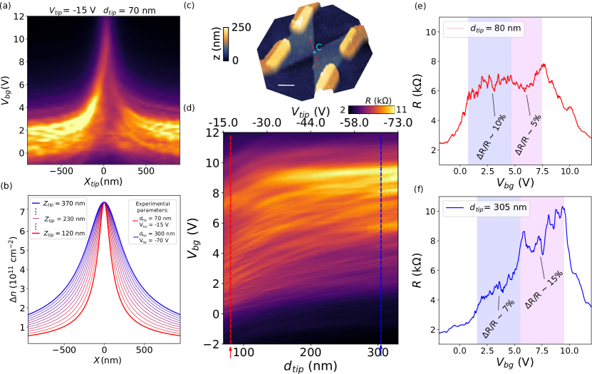
The biased SGM tip locally changes the carrier density , leading to a Lorentzian evolution of , centered at the tip position. When placing the tip at the center of the constriction, a n-p-n or p-n-p configuration can be reached, depending on the tip voltage and backgate voltage . This is illustrated in Figure 1c showing resistance as a function of and for a tip-to graphene distance = 70 nm, The n-p-n region, located at the lower left part of Fig. 1c, is decorated with a complex pattern of interleaved fringes, resulting from different types of interference phenomena. In the investigated geometry, one can indeed anticipate that, beside the tip-induced n-p-n or p-n-p junction, other confinements play a role and contribute to interferences in the map shown in Fig. 1c, such as the constriction defined by etching. Fortunately, increasing the tip-graphene distance to = 200 nm yields a clearer picture, shown in Fig. 1d, with a much simpler fringe pattern (most of them essentially parallel to the n-p-n/n-n’-n limit). The visibility of the pattern is also enhanced by their stronger contrast, when compared to the pattern in Fig. 1c. In Figure 1b, we plot two profiles of resistance versus , for = 70 nm (red curve) and = 200 nm (blue curve) where is adapted to reach comparable tip-induced density change (respectively -13 V and -35 V). From this figure, the contrast of the oscillations appears clearly higher for a larger , and a detailed discussion of the origin of this contrast enhancement is one of the main focus of this paper.
It shall first be clarified that these oscillations correspond indeed to Fabry-Pérot interferences arising inside the tip-induced n-p-n region. Figures 1e and 1f (recorded during a different cooldown) illustrate the sensitivity of these interference fringes to a perpendicular magnetic field. Figure 1e presents the interference pattern recorded by placing the tip above the constriction center ( = 100 nm). The map in Fig. 1e displays the derivative of versus to highlight the interference fringes, that appear similar to the ones observed in Fig. 1c-d. Fig. 1f shows that they have completely disappeared at a perpendicular magnetic field of 800 mT. From their characteristic decay field, one can infer that these fringes can be associated with a characteristic length, corresponding to a few hundreds nanometer-long cavity, compatible with the cavity formed in the tip induced n-p-n region, as sketched in the inset of Fig. 1b (see supplementary data for additional data and a more detailed discussion). In addition, an accurate determination of the tip-induced potential and an analytical calculation yielding the expected resonances positions in this potential profile agree well with the observed oscillations evolution, as detailed below. All these considerations provide strong evidence that the oscillations correspond to Fabry-Pérot oscillation in the tip-induced n-p-n region. In the remainder of this paper, we will discuss these interference fringes (Fig. 1c-e) and show that their visibility depends on the smoothness of the p-n junction, controlled by .
As a first step, one needs to precisely evaluate the tip-induced potential. This is done by scanning the tip along the blue dashed line Fig. 2c while varying , at fixed and tip-to-graphene distance (i.e. the same procedure described in ref. Brun et al. (2019)). The resulting conductance map shown in Fig. 2a exhibits a resistance maximum that follows a Lorentzian shape, as the tip crosses the center of the constriction. This shape is directly related to the shape of the tip-induced potential, as it corresponds to the tip-induced change in the energy of the charge neutrality point at the location of the constriction, which governs the device resistance. Repeating this experiment for several values of , and adapting to keep a constant maximum density change below the tip , we can fit the different density profiles under the tip influence, provided that the -axis is properly scaled to a density using the backgate lever-arm parameter (see supplementary data).
Considering the tip as a point charge, the expected tip-induced density change would write: , where is the horizontal distance to the tip center, and is the effective tip-to-graphene distance, i.e. = , being the tip radius (a = 50 nm). We define as the half-width at half-maximum (HWHM) of this density profile, that is in this expression given by the effective tip height . Note that this textbook model underestimates the long-range tail of the tip-induced density change (see supplementary data). Accurately modeling the tip-induced potential yields a complex electrostatic problem Zhang and Fogler (2008); Żebrowski et al. (2018); Chaves et al. (2019), which is beyond the scope of the present paper. In turn, we model with the following phenomenological equation: , where we assume that the HWHM is given by and is therefore known in the experiment, the only free parameter being . Fig. 2b shows estimates of tip-induced density changes, for different couples of and leading to the same (see supplementary data and movie for details).
To study the influence of this potential extension on the Fabry-Pérot oscillations, we place the polarized tip on top of the constriction center (point C in Fig. 2c),
and record the resistance as a function of , for different tip-to-graphene distance . As is increased, we decrease (towards more negative
values) to keep a constant value of , and vary only the smoothness of the p-n junctions through .
The resulting resistance map is plotted in Fig. 2d and constitutes the main result of this study, together with its detailed theoretical analysis.
Figures 2e and 2f show the device resistance as a function of , for two extreme values of in Fig. 2d.
These two plots highlight two main features already visible in Fig. 2d, i.e.:
(i) The maximum value of the resistance increases with increasing as well as the density for which this maximum is reached.
(ii) The contrast of the Fabry-Pérot interference evolves in a different way for the lower energy modes observed at low
(they decrease in amplitude) and the higher energy ones, whose amplitude increases with .
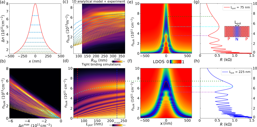
In order to understand these observations, we analyze the problem with two different approaches. The first one is analytic: we use the potential landscape evaluated from Fig. 2a and 2b, and follow the approach proposed in Ref.Drienovsky et al. (2014) . We consider the tip potential as varying only along x-axis, and evaluate the position of the expected resonances from the simple equal phase condition:
| (1) |
where is the position of zero charge density along x-axis which depends on the bulk density , p is a positive integer, and is the position-dependent wave-vector evaluated from provided that . Fig. 3a shows a typical tip-induced density change and the position of the first resonant modes. In Fig. 3b, we calculate the expected position of the 10 first resonant modes for a tip potential extension of 250 nm as a function of and , and report them as dashed lines on top of the experimental data of Fig. 1d (where we have used the backgate and tip lever-arm parameters to convert the and axis into carrier densities). There is a good qualitative correspondence between the evolution of the different modes and the experimental fringes, reinforcing the interpretation of their origin as Fabry-Pérot resonances inside the tip-induced n-p-n region. Using measured for the different couples of and , displayed in Fig. 2b, we also plot in Fig. 3c the evolution of the first 15 modes in the (,) plane, and find that they fall nicely on top of the experimental data of Fig. 2d, rescaling the vertical axis to a density and the horizontal axes and to the tip potential extension .
To go one step further in the understanding of the experimental fringes, we perform tight-binding simulations, using a home-made recursive Green functions code Nguyen et al. (2010). We study a simple graphene ribbon, to which we apply a potential of variable extension along transport direction, (see inset of Fig. 3g), with a smoothness governed by the exponent :
| (2) |
The ribbon width is fixed to 800 nm to avoid undesirable effects of transverse quantization (Fabry-Pérot resonances are insensitive to the ribbon width). We first consider a Lorentzian potential with = 2, and calculate the ribbon resistance as a function of bulk density (i.e. the charge carrier density in the p region) and potential extension , while keeping a fixed value of = . The result is plotted in Fig. 3d. First of all, it should be noted that the first resistance maximum (cyan dotted line on Fig. 3d) is not obtained for = (green dotted line). This is clarified in Fig. 3e, where we plot the local density of states (LDOS) in the graphene ribbon integrated over the transverse direction, as a function of , aside with the resistance as a function of bulk density (Fig. 3g), for a potential extension = 75 nm. There is indeed a clear offset between the bulk density corresponding to the maximum of the tip-induced potential in Fig. 3e (indicated by a green dotted line) and the resistance maximum in Fig. 3g (indicated by a cyan dotted line). The resistance maximum is rather reached for a density yielding a minimum LDOS at the barrier center.
Figures 3f and 3h present the same analysis for a larger potential extension. In this case, the bulk densities corresponding to (in green) and to the minimum LDOS (in cyan) are closer to each other, but still do not match. The respective evolution of these two densities with the potential extension can be followed Fig. 3d, as the spacing between the green and cyan dotted lines, and is in good agreement with the evolution of the resistance maximum observed in the experiment, as visible in figures 2d and 3c.
A second interesting feature well captured by this toy model is the evolution of the first resonant mode energy, visible as the first resistance minimum indicated by purple dashed lines in Figs.3e-h, which follows roughly the same average evolution as the resistance maximum. This first Fabry-Pérot mode energy is reminiscent of the confinement energy due to the potential well created by the tip. In quantum mechanics, a famous textbook problem consists in finding the zero-point energy of a “particle-in-a-box”, i.e. trapped in an infinite square potential of length . The zero-point energy in the latter case emerges as a consequence of Heisenberg uncertainty principle, and increases with decreasing (as for massive particles and for massless Dirac fermions Cho and Fuhrer (2011)). This distance of the first mode to the maximum of the tip potential is also clearly dependent on in the experiment, as visible ine Figs.2d and 3c. It provides a nice illustration of this textbook problem, poorly explored in the case of Dirac fermions due to the inherent difficulty to confine them.
Discrepancies are however visible between results from this ideal ribbon model and experimental data. First of all, additional resonances are present in the experiment. They could result from the transverse quantization inherent to the narrow constriction, intentionally suppressed in the tight-binding model by simulating a wide ribbon. These additional resonances could also arise from disorder, and the finite distance between the contacts and the constriction, that could lead to other Fabry-Pérot cavities. Secondly, the high resistance at low bulk density in the model is not present in the experiment. This can easily be understood as due to the experimentally measured finite resistance at the Dirac point, inherent to residual electron-hole puddles at low densities, whereas the tight-binding calculation in a homogeneous graphene ribbon predicts a much larger resistance of the bulk (and leads) close to the Dirac point. Both effects prevent the direct quantitative comparison of the interferences contrast in the experiment and the model presented in Fig. 3.
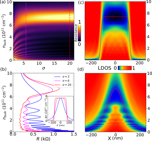
To better understand the influence of the tip potential extension, we perform additional tight-binding simulations and vary the potential steepness by changing the decay exponent in equation (2). We first calculate the resistance of the ribbon as a function of bulk density and decay exponent, and plot the result in Fig. 4a. For three different decay exponents ( = 2,6,20) we extract the resistance as a function of and plot the result in Fig. 4b. These two figures evidence that the potential smoothness is a key ingredient, that governs the Fabry-Pérot interference contrast. Indeed, the relativistic nature of graphene charge carriers makes sharp potential barriers highly transparent due to Klein tunneling. As a consequence, the Fabry-Pérot resonances in the LDOS are rather large and overlap (see Fig. 4c), owing to their hybridization with the Dirac continuum of the bulk. This weak confinement yields poorly contrasted Fabry-Pérot oscillations in the total resistance (red curve Fig. 4b). In contrast, a smooth p-n junction (on the Fermi wavelength scale) is a poor Dirac fermions transmitter, so that two facing smooth p-n junctions can be used to confine Dirac fermions in a more efficient way. This can be seen Fig. 4d, where the LDOS in the case of a smooth n-p-n junction is plotted, and exhibits well defined resonant modes, giving rise to pronounced Fabry-Pérot oscillations in the resistance (blue curve Fig. 4b).
The confinement of Dirac fermions in p-n nano-islands and the resulting LDOS resonances have recently been explored in a set of beautiful scanning tunneling microscopy experiments Gutiérrez et al. (2016); Zhao et al. (2015); Lee et al. (2016); Jiang et al. (2017). Although our SGM experiment does not give direct access to the LDOS, it allows to probe transport through such islands and reveals the strength of LDOS resonances through Fabry-Pérot oscillations in the device resistance. Tight-binding simulations explicitly confirm that the interference contrast is related to the LDOS resonances strength, themselves governed by the p-n junction smoothness, which can be easily tuned in SGM, as demonstrated here.
In conclusion, we defined a n-p-n junction in a high mobility graphene sample using the polarized tip of a scanning gate microscope. Oscillating patterns are observed in transport through the n-p-n junction that can be attributed to Fabry-Pérot interferences. By simultaneously varying the tip-to-graphene distance and tip voltage, one can control and characterize the p-n junctions smoothness. In turn, this allowed to show that smoother p-n junctions induce a larger contrast of the interference fringes. Using tight-binding simulations, we studied the influence of the p-n junctions smoothness on the LDOS resonances, resulting from the quasi-confinement of Dirac fermions within the tip-induced potential. These LDOS resonances amplitude can be explicitly linked to the visibility of the Fabry-Pérot oscillations. In the quest towards ever reduced graphene devices size, gates are often placed as close as possible to the graphene plane. The present study recalls that the gate dielectric thickness governs the p-n junction smoothness, which strongly influences the visibility of interferences. It then governs the efficiency of devices based on electron-optics concepts. This underlines that these distances have to be cleverly adjusted in the conception of relativistic electron optics devices.
Acknowledgments
The present research was funded by the Fédération Wallonie-Bruxelles through the ARC Grant on 3D nanoarchitecturing of 2D crystals (No. 16/21-077) and from the European Union’s Horizon 2020 Research and Innovation program (No. 696656). B.B. (research assistant), N.M. (FRIA fellowship), B.H. (research associate), V.-H.N. and J.-C.C. (PDR No. T.1077.15 and ERA-Net No. R.50.07.18.F) acknowledge financial support from the F.R.S.-FNRS of Belgium. Support by the Helmholtz Nanoelectronic Facility (HNF), the EU ITN SPINOGRAPH and the DFG (SPP-1459) is gratefully acknowledged. Growth of hexagonal boron nitride crystals was supported by the Elemental Strategy Initiative conducted by the MEXT, Japan and JSPS KAKENHI Grant Numbers JP26248061, JP15K21722 and JP25106006. B.B aknowledges the use of Kwant Groth et al. (2014) used to guide the experiment and cross-check tight-binding simulations.
References
References
- Novoselov et al. (2005) K. S. Novoselov, A. K. Geim, S. V. Morozov, D. Jiang, M. I. Katsnelson, I. V. Grigorieva, S. V. Dubonos, and A. A. Firsov, Nature 438, 197 (2005).
- Klein (1929) O. Klein, Zeitschrift für Physik 53, 157 (1929).
- Allain and Fuchs (2011) P. E. Allain and J. N. Fuchs, The European Physical Journal B 83, 301 (2011).
- Cheianov et al. (2007) V. V. Cheianov, V. Fal’ko, and B. L. Altshuler, Science 315, 1252 (2007).
- Milovanović et al. (2015) S. P. Milovanović, D. Moldovan, and F. M. Peeters, Journal of Applied Physics 118, 154308 (2015).
- Veselago (1968) V. G. Veselago, Soviet Physics Uspekhi 10, 509 (1968).
- Beenakker et al. (2009) C. W. J. Beenakker, R. A. Sepkhanov, A. R. Akhmerov, and J. Tworzydło, Phys. Rev. Lett. 102, 146804 (2009).
- Hartmann et al. (2010) R. R. Hartmann, N. J. Robinson, and M. E. Portnoi, Phys. Rev. B 81, 245431 (2010).
- Williams et al. (2011) J. R. Williams, T. Low, M. S. Lundstrom, and C. M. Marcus, Nature Nanotechnology 6, 222 (2011).
- Rickhaus et al. (2015) P. Rickhaus, M.-H. Liu, P. Makk, R. Maurand, S. Hess, S. Zihlmann, M. Weiss, K. Richter, and C. Schönenberger, Nano Letters 15, 5819 (2015).
- Cserti et al. (2007) J. Cserti, A. Pályi, and C. Péterfalvi, Phys. Rev. Lett. 99, 246801 (2007).
- Mu et al. (2011) W. Mu, G. Zhang, Y. Tang, W. Wang, and Z. Ou-Yang, Journal of Physics: Condensed Matter 23, 495302 (2011).
- Garg et al. (2014) N. A. Garg, S. Ghosh, and M. Sharma, Journal of Physics: Condensed Matter 26, 155301 (2014).
- Wu and Fogler (2014) J.-S. Wu and M. M. Fogler, Phys. Rev. B 90, 235402 (2014).
- Logemann et al. (2015) R. Logemann, K. J. A. Reijnders, T. Tudorovskiy, M. I. Katsnelson, and S. Yuan, Phys. Rev. B 91, 045420 (2015).
- Lu and Zhang (2018) M. Lu and X.-X. Zhang, Journal of Physics: Condensed Matter 30, 215303 (2018).
- Zhang et al. (2018) S.-H. Zhang, W. Yang, and F. M. Peeters, Phys. Rev. B 97, 205437 (2018).
- Liu et al. (2017) M.-H. Liu, C. Gorini, and K. Richter, Phys. Rev. Lett. 118, 066801 (2017).
- Bøggild et al. (2017) P. Bøggild, J. M. Caridad, C. Stampfer, G. Calogero, N. R. Papior, and M. Brandbyge, Nature Communications 8, 15783 (2017), article.
- Shytov et al. (2008) A. V. Shytov, M. S. Rudner, and L. S. Levitov, Phys. Rev. Lett. 101, 156804 (2008).
- Young and Kim (2009) A. F. Young and P. Kim, Nature Physics 5, 222 (2009).
- Velasco et al. (2009) J. Velasco, G. Liu, W. Bao, and C. N. Lau, New Journal of Physics 11, 095008 (2009).
- Nam et al. (2011) S.-G. Nam, D.-K. Ki, J. W. Park, Y. Kim, J. S. Kim, and H.-J. Lee, Nanotechnology 22, 415203 (2011).
- Rickhaus et al. (2013) P. Rickhaus, R. Maurand, M.-H. Liu, M. Weiss, K. Richter, and C. Schönenberger, Nature Communications 4, 2342 (2013), article.
- Oksanen et al. (2014) M. Oksanen, A. Uppstu, A. Laitinen, D. J. Cox, M. F. Craciun, S. Russo, A. Harju, and P. Hakonen, Phys. Rev. B 89, 121414 (2014).
- Handschin et al. (2017) C. Handschin, P. Makk, P. Rickhaus, M.-H. Liu, K. Watanabe, T. Taniguchi, K. Richter, and C. Schönenberger, Nano Letters 17, 328 (2017).
- Veyrat et al. (2019) L. Veyrat, A. Jordan, K. Zimmermann, F. Gay, K. Watanabe, T. Taniguchi, H. Sellier, and B. Sacépé, Nano Letters 19, 635 (2019).
- Varlet et al. (2014) A. Varlet, M.-H. Liu, V. Krueckl, D. Bischoff, P. Simonet, K. Watanabe, T. Taniguchi, K. Richter, K. Ensslin, and T. Ihn, Phys. Rev. Lett. 113, 116601 (2014).
- Campos et al. (2012) L. C. Campos, A. F. Young, K. Surakitbovorn, K. Watanabe, T. Taniguchi, and P. Jarillo-Herrero, Nature Communications 3, 1239 EP (2012), article.
- Morikawa et al. (2017) S. Morikawa, Q. Wilmart, S. Masubuchi, K. Watanabe, T. Taniguchi, B. Plaçais, and T. Machida, Semiconductor Science and Technology 32, 045010 (2017).
- Graef et al. (2019) H. Graef, Q. Wilmart, M. Rosticher, D. Mele, L. Banszerus, C. Stampfer, T. Taniguchi, K. Watanabe, J.-M. Berroir, E. Bocquillon, G. Fève, E. H. T. Teo, and B. Plaçais, Nature Communications 10, 2428 (2019).
- Wang et al. (2019) K. Wang, M. M. Elahi, L. Wang, K. M. M. Habib, T. Taniguchi, K. Watanabe, J. Hone, A. W. Ghosh, G.-H. Lee, and P. Kim, Proceedings of the National Academy of Sciences 116, 6575 (2019), https://www.pnas.org/content/116/14/6575.full.pdf .
- Eriksson et al. (1996) M. A. Eriksson, R. G. Beck, M. Topinka, J. A. Katine, R. M. Westervelt, K. L. Campman, and A. C. Gossard, Applied Physics Letters 69, 671 (1996).
- Topinka et al. (2001) M. A. Topinka, B. J. LeRoy, R. M. Westervelt, S. E. J. Shaw, R. Fleischmann, E. J. Heller, K. D. Maranowski, and A. C. Gossard, Nature 410, 183 (2001).
- Jura et al. (2009) M. P. Jura, M. A. Topinka, M. Grobis, L. N. Pfeiffer, K. W. West, and D. Goldhaber-Gordon, Phys. Rev. B 80, 041303 (2009).
- Kozikov et al. (2013) A. A. Kozikov, C. Rössler, T. Ihn, K. Ensslin, C. Reichl, and W. Wegscheider, New Journal of Physics 15, 013056 (2013).
- Brun et al. (2014) B. Brun, F. Martins, S. Faniel, B. Hackens, G. Bachelier, A. Cavanna, C. Ulysse, A. Ouerghi, U. Gennser, D. Mailly, S. Huant, V. Bayot, M. Sanquer, and H. Sellier, Nat. Commun. 5, 4290 (2014).
- Schnez et al. (2010) S. Schnez, J. Güttinger, M. Huefner, C. Stampfer, K. Ensslin, and T. Ihn, Phys. Rev. B 82, 165445 (2010).
- Pascher et al. (2012) N. Pascher, D. Bischoff, T. Ihn, and K. Ensslin, Applied Physics Letters 101, 063101 (2012), http://dx.doi.org/10.1063/1.4742862.
- Garcia et al. (2013) A. G. F. Garcia, M. König, D. Goldhaber-Gordon, and K. Todd, Phys. Rev. B 87, 085446 (2013).
- Cabosart et al. (2017) D. Cabosart, A. Felten, N. Reckinger, A. Iordanescu, S. Toussaint, S. Faniel, and B. Hackens, Nano Letters 17, 1344 (2017).
- Bhandari et al. (2016) S. Bhandari, G.-H. Lee, A. Klales, K. Watanabe, T. Taniguchi, E. Heller, P. Kim, and R. M. Westervelt, Nano Letters 16, 1690 (2016).
- Xiang et al. (2016) S. Xiang, A. Mreńca-Kolasińska, V. Miseikis, S. Guiducci, K. Kolasiński, C. Coletti, B. Szafran, F. Beltram, S. Roddaro, and S. Heun, Phys. Rev. B 94, 155446 (2016).
- Mreńca-Kolasińska and Szafran (2015) K. Mreńca-Kolasińska, A.; Kolasiński and B. Szafran, Semiconductor Science and Technology 30, 085003 (2015).
- Mreńca-Kolasińska et al. (2016) A. Mreńca-Kolasińska, S. Heun, and B. Szafran, Phys. Rev. B 93, 125411 (2016).
- Mreńca-Kolasińska and Szafran (2017) A. Mreńca-Kolasińska and B. Szafran, Phys. Rev. B 96, 165310 (2017).
- Petrović et al. (2017) M. D. Petrović, S. P. Milovanović, and F. M. Peeters, Nanotechnology 28, 185202 (2017).
- Dou et al. (2018) Z. Dou, S. Morikawa, A. Cresti, S.-W. Wang, C. G. Smith, C. Melios, O. Kazakova, K. Watanabe, T. Taniguchi, S. Masubuchi, T. Machida, and M. R. Connolly, Nano Letters 18, 2530 (2018).
- Brun et al. (2019) B. Brun, N. Moreau, S. Somanchi, V.-H. Nguyen, K. Watanabe, T. Taniguchi, J.-C. Charlier, C. Stampfer, and B. Hackens, Phys. Rev. B 100, 041401 (2019).
- Terrés et al. (2016) B. Terrés, L. A. Chizhova, F. Libisch, J. Peiro, D. Jörger, S. Engels, A. Girschik, K. Watanabe, T. Taniguchi, S. V. Rotkin, J. Burgdörfer, and C. Stampfer, Nature Communications 7, 11528 (2016), article.
- Hackens et al. (2010) B. Hackens, F. Martins, S. Faniel, C. A. Dutu, H. Sellier, S. Huant, M. Pala, L. Desplanque, X. Wallart, and V. Bayot, Nat. Commun. 1, 39 (2010).
- Zhang and Fogler (2008) L. M. Zhang and M. M. Fogler, Phys. Rev. Lett. 100, 116804 (2008).
- Żebrowski et al. (2018) D. Żebrowski, A. Mreńca-Kolasińska, and B. Szafran, Phys. Rev. B 98, 155420 (2018).
- Chaves et al. (2019) F. A. Chaves, D. Jiménez, J. E. Santos, P. Bøggild, and J. M. Caridad, Nanoscale 11, 10273 (2019).
- Drienovsky et al. (2014) M. Drienovsky, F.-X. Schrettenbrunner, A. Sandner, D. Weiss, J. Eroms, M.-H. Liu, F. Tkatschenko, and K. Richter, Phys. Rev. B 89, 115421 (2014).
- Nguyen et al. (2010) V. H. Nguyen, A. Bournel, and P. Dollfus, Journal of Physics: Condensed Matter 22, 115304 (2010).
- Cho and Fuhrer (2011) S. Cho and M. Fuhrer, Nano Research 4, 385 (2011).
- Gutiérrez et al. (2016) C. Gutiérrez, L. Brown, C.-J. Kim, J. Park, and A. N. Pasupathy, Nature Physics 12, 1069 EP (2016), article.
- Zhao et al. (2015) Y. Zhao, J. Wyrick, F. D. Natterer, J. F. Rodriguez-Nieva, C. Lewandowski, K. Watanabe, T. Taniguchi, L. S. Levitov, N. B. Zhitenev, and J. A. Stroscio, Science 348, 672 (2015).
- Lee et al. (2016) J. Lee, D. Wong, J. Velasco Jr, J. F. Rodriguez-Nieva, S. Kahn, H.-Z. Tsai, T. Taniguchi, K. Watanabe, A. Zettl, F. Wang, L. S. Levitov, and M. F. Crommie, Nature Physics 12, 1032 (2016).
- Jiang et al. (2017) Y. Jiang, J. Mao, D. Moldovan, M. R. Masir, G. Li, K. Watanabe, T. Taniguchi, F. M. Peeters, and E. Y. Andrei, Nature Nanotechnology 12, 1045 (2017).
- Groth et al. (2014) C. W. Groth, M. Wimmer, A. R. Akhmerov, and X. Waintal, New Journal of Physics 16, 063065 (2014).
![[Uncaptioned image]](/html/1911.12031/assets/x5.png)
![[Uncaptioned image]](/html/1911.12031/assets/x6.png)
![[Uncaptioned image]](/html/1911.12031/assets/x7.png)
![[Uncaptioned image]](/html/1911.12031/assets/x8.png)
![[Uncaptioned image]](/html/1911.12031/assets/x9.png)
![[Uncaptioned image]](/html/1911.12031/assets/x10.png)