Slow light, double directional rainbow trapping and releasing at terahertz frequencies

Jie Xu,1,2,3,8 Qian Shen2,4,8, Kai Yuan,4 Xiaohua Deng,2 Yun Shen,2,5 Hang Zhang,6 Chiaho Wu,6 Sanshui Xiao,3,7 and Linfang Shen2,6,*


1 College of Material Science and Engineering, Nanchang University, Nanchang 330031, China
2 Institute of Space Science and Technology, Nanchang University, Nanchang 330031, China
3 Department of Photonics Engineering, Technical University of Denmark, DK-2800 Kgs. Lyngby, Denmark
4 School of Information Engineer, Nanchang University, Nanchang, 330031, China
5 Department of Physics, Nanchang University, Nanchang 330031, China
6 Department of Applied Physics, Zhejiang University of Technology, Hangzhou 310023, China
7 Center for Nanostructured Graphene, Technical University of Denmark, DK-2800 Kgs. Lyngby, Denmark
8 These authors contributed equally to the work

* lfshen@zjut.edu.cn

Abstract

Slow light and rainbow trapping attract many attentions in last twenty years, and in most of the previous works, the researchers achieve the slow light and rainbow trapping with complicate configurations or techniques, for example, metamaterial techniques. In this paper, we propose a simple waveguide consisted with semiconductor and dielectric layers, and we find that the slow-light peaks appear in the dispersion curves. Besides, the cutoff frequency with vg=0subscript𝑣𝑔0v_{g}=0 (vgsubscript𝑣𝑔v_{g} is the group velocity) in the slow-light peaks is depending on the thicknesses of the semiconductor and dielectric. Then, we design a tapered, horizontally symmetric structure. By using software COMSOL and finite difference time domain method as well, we achieve double directional rainbow trapping and more importantly, releasing the rainbow in such structure. This approach is promising for optical isolator, optical buffer, optical switch and other optical functional devices in miniaturization optical integrated circuit.

1 Introduction

Surface magnetoplasmon (SMP) is sustained at the interface of a magnetic-optical (MO) material and a dielectric material, and it will behave the one-way propagating property when applying a dc external magnetic field on the MO material. The one-way SMP is similar to the chiral edge states founded in the quantum-Hall effect [1]. In 2008, F. D. M. Haldane and S. Raghu showed the possibility of one-way waveguide in photonic crystals (PCs)[2], and in the next year, Wang and his colleagues experimentally observed the one-way SMP in a PC consisted of gyromagnetic yttrium-iron-garnet (YIG) in microwave regime[3]. Since then, one-way SMP draws more and more attentions[4, 5, 6, 7].

Manipulating the light always attracts the physicists and slowing light is one of the most interesting and meaningful part because of its potential applications in energy storage[8, 9, 10], enhancing nonlinearity[11, 12, 13], quantum optics[14, 15]. At the very beginning, people study the slow-light by using electromagnetically induced transparency (EIT) which is excellent for fundamental investigations, but is unsuitable for practical applications[16, 17]. In the past decades, lots of researchers are trying to slow light in PCs by introducing defects and the photonic bandgap (PBG)[18, 19, 11, 20], and others used the metamaterials[8]. Recently, we proposed a simple tapered metal-dielectric-semiconductor-metal (MDSM) structure in terahertz regime[21], and we proved that this MDSM structure is capable for slowing light (SMP) and trapping ’rainbow’.

In this paper, we propose a metal-dielectric-semiconductor-dielectric-metal (MDSDM) structure and theoretically study the propagation properties in the MDSDM model. After carefully investigation, we find that the dispersion properties of the SMPs in the MDSDM model is manipulable by changing the thicknesses of the dielectric and the semiconductor layers. Based on our theory, we design a tapered, horizontal symmetric waveguide and by using the software COMSOL and finite difference time domain (FDTD) method, for the first time, we present the double directional slow light, rainbow trapping and releasing in terahertz regime. Our work is promising for optical functional devices.

2 Physical model and slow light

Refer to caption
Figure 1: (a) The schematic of the MDSDM structure. (b) The dispersion curves of SMPs. Red lines: D1=(0.025​λp,0.025​λp)subscript𝐷10.025subscriptπœ†π‘0.025subscriptπœ†π‘D_{1}=(0.025\lambda_{p},0.025\lambda_{p}); Cyan lines: D2=(0.025​λp,0.006​λp)subscript𝐷20.025subscriptπœ†π‘0.006subscriptπœ†π‘D_{2}=(0.025\lambda_{p},0.006\lambda_{p}). The solid and dashed lines are respectively represent the SMPs sustained on interfaces 1 and 2. (c) The group velocity (vgsubscript𝑣𝑔v_{g}) of the upper branches of SMPs dispersion curves in (b) for kβ‰₯0π‘˜0k\geq 0. The yellow shaded areas are the asymptotic frequencies band and the green shaded areas represent the bulk zones of the semiconductor. The waveguide parameter D=(d1,d2)𝐷subscript𝑑1subscript𝑑2D=(d_{1},d_{2}). The other parameters are Ξ΅r=11.68subscriptπœ€π‘Ÿ11.68\varepsilon_{r}=11.68, Ρ∞=15.6subscriptπœ€15.6\varepsilon_{\infty}=15.6 and Ο‰c=0.1​ωpsubscriptπœ”π‘0.1subscriptπœ”π‘\omega_{c}=0.1\omega_{p}.

We first investigate the dispersion relation of the SMPs in the metal-dielectric-semiconductor-dielectric-metal (MDSDM) waveguide shown in Fig. 1(a). We note that, in the terahertz regime, metal can be regarded as perfect electric conductor (PEC)[22] and only the transverse magnetic (TM) modes can propagate along dielectric-semiconductor interfaces. The (relative) permittivity of the semiconductor (in this paper we assume the semiconductor is Insb and the dielectric is Si) under a dc magnetic field (B0subscript𝐡0B_{0}) has the form[23]

πœ€β†”=[Ξ΅1βˆ’i​Ρ20i​Ρ2Ξ΅1000Ξ΅3],superscriptπœ€β†”delimited-[]subscriptπœ€1𝑖subscriptπœ€20missing-subexpressionmissing-subexpressionmissing-subexpressionmissing-subexpressionmissing-subexpressionmissing-subexpressionmissing-subexpressionmissing-subexpressionmissing-subexpressionmissing-subexpressionmissing-subexpressionmissing-subexpressionmissing-subexpressionmissing-subexpressionmissing-subexpressionmissing-subexpressionmissing-subexpression𝑖subscriptπœ€2subscriptπœ€10missing-subexpressionmissing-subexpressionmissing-subexpressionmissing-subexpressionmissing-subexpressionmissing-subexpressionmissing-subexpressionmissing-subexpressionmissing-subexpressionmissing-subexpressionmissing-subexpressionmissing-subexpressionmissing-subexpressionmissing-subexpressionmissing-subexpressionmissing-subexpressionmissing-subexpression00subscriptπœ€3missing-subexpressionmissing-subexpressionmissing-subexpressionmissing-subexpressionmissing-subexpressionmissing-subexpressionmissing-subexpressionmissing-subexpressionmissing-subexpressionmissing-subexpressionmissing-subexpressionmissing-subexpressionmissing-subexpressionmissing-subexpressionmissing-subexpressionmissing-subexpressionmissing-subexpression\mathop{\varepsilon}\limits^{\leftrightarrow}=\left[{\begin{array}[]{*{20}{c}}{{\varepsilon_{1}}}&{-i{\varepsilon_{2}}}&0\\ {i{\varepsilon_{2}}}&{{\varepsilon_{1}}}&0\\ 0&0&{{\varepsilon_{3}}}\end{array}}\right], (1a)
Ξ΅1=Ξ΅βˆžβ€‹(1βˆ’Ο‰p2Ο‰2βˆ’Ο‰c2),Ξ΅2=Ξ΅βˆžβ€‹Ο‰c​ωp2ω​(Ο‰2βˆ’Ο‰c2),Ξ΅3=Ξ΅βˆžβ€‹(1βˆ’Ο‰p2Ο‰2),formulae-sequencesubscriptπœ€1subscriptπœ€1superscriptsubscriptπœ”π‘2superscriptπœ”2superscriptsubscriptπœ”π‘2formulae-sequencesubscriptπœ€2subscriptπœ€subscriptπœ”π‘superscriptsubscriptπœ”π‘2πœ”superscriptπœ”2superscriptsubscriptπœ”π‘2subscriptπœ€3subscriptπœ€1superscriptsubscriptπœ”π‘2superscriptπœ”2\varepsilon_{1}=\varepsilon_{\infty}\left({1-\frac{{\omega_{p}^{2}}}{{\omega^{2}-\omega_{c}^{2}}}}\right),\varepsilon_{2}=\varepsilon_{\infty}\frac{{\omega_{c}\omega_{p}^{2}}}{{\omega(\omega^{2}-\omega_{c}^{2})}},\varepsilon_{3}=\varepsilon_{\infty}\left({1-\frac{{\omega_{p}^{2}}}{{\omega^{2}}}}\right), (1b)
Ξ΅1=Ξ΅βˆžβ€‹(1βˆ’(Ο‰+i​v)​ωp2ω​[(Ο‰+i​v)2βˆ’Ο‰c2]),Ξ΅2=Ξ΅βˆžβ€‹Ο‰c​ωp2ω​[(Ο‰+i​v)2βˆ’Ο‰c2],Ξ΅3=Ξ΅βˆžβ€‹(1βˆ’Ο‰p2ω​(Ο‰+i​v)),formulae-sequencesubscriptπœ€1subscriptπœ€1πœ”π‘–π‘£superscriptsubscriptπœ”π‘2πœ”delimited-[]superscriptπœ”π‘–π‘£2superscriptsubscriptπœ”π‘2formulae-sequencesubscriptπœ€2subscriptπœ€subscriptπœ”π‘superscriptsubscriptπœ”π‘2πœ”delimited-[]superscriptπœ”π‘–π‘£2superscriptsubscriptπœ”π‘2subscriptπœ€3subscriptπœ€1superscriptsubscriptπœ”π‘2πœ”πœ”π‘–π‘£\varepsilon_{1}=\varepsilon_{\infty}\left(1-\frac{\left(\omega+iv\right)\omega_{p}^{2}}{\omega\left[\left(\omega+iv\right)^{2}-\omega_{c}^{2}\right]}\right),\;\varepsilon_{2}=\varepsilon_{\infty}\frac{\omega_{c}\omega_{p}^{2}}{\omega\left[\left(\omega+iv\right)^{2}-\omega_{c}^{2}\right]},\varepsilon_{3}=\varepsilon_{\infty}\left(1-\frac{\omega_{p}^{2}}{\omega\left(\omega+iv\right)}\right), (1c)

where Ο‰πœ”\omega, Ο‰psubscriptπœ”π‘\omega_{p}, Ο‰c=e​B0/mβˆ—subscriptπœ”π‘π‘’subscript𝐡0superscriptπ‘š\omega_{c}=eB_{0}/m^{*}, e𝑒e, mβˆ—superscriptπ‘šm^{*} and Ρ∞subscriptπœ€\varepsilon_{\infty} are the angular frequency, the plasma frequency, the electron cyclotron frequency, the charge of a electron, the effective mass of a electron and the high-frequency (relative) permittivity of the semiconductor, respectively. Eq. (1c) is the permittivity of the semiconductor in loss condition and ν𝜈\nu is the electron scattering frequency. We analysis the dispersion relation in lossless condition and in the simulations below, we will show that the propagation properties in loss condition fit well with the lossless condition. Based on the Maxwell’s equations and the boundary conditions, one can easily obtain the dispersion relation of the SMPs in the MDSDM model, and it can be written as

2​Ρv​α1Ξ΅r​tanh⁑(Ξ±1​d1)+Aα​tanh⁑(2​α​d2)=0,2subscriptπœ€π‘£subscript𝛼1subscriptπœ€π‘Ÿsubscript𝛼1subscript𝑑1𝐴𝛼2𝛼subscript𝑑20\frac{2\varepsilon_{v}\alpha_{1}}{\varepsilon_{r}}\tanh(\alpha_{1}d_{1})+\frac{A}{\alpha}\tanh(2\alpha d_{2})=0, (2a)
A=(2​Ρv​α1Ξ΅r​tanh⁑(Ξ±1​d1))2βˆ’(Ξ΅2Ξ΅1​k)2+Ξ±2𝐴superscript2subscriptπœ€π‘£subscript𝛼1subscriptπœ€π‘Ÿsubscript𝛼1subscript𝑑12superscriptsubscriptπœ€2subscriptπœ€1π‘˜2superscript𝛼2A=(\frac{2\varepsilon_{v}\alpha_{1}}{\varepsilon_{r}}\tanh{(\alpha_{1}d_{1}))}^{2}-(\frac{\varepsilon_{2}}{\varepsilon_{1}}k)^{2}+\alpha^{2} (2b)

where Ξ΅v=Ξ΅1βˆ’Ξ΅22Ξ΅1subscriptπœ€π‘£subscriptπœ€1superscriptsubscriptπœ€22subscriptπœ€1\varepsilon_{v}=\varepsilon_{1}-\frac{\varepsilon_{2}^{2}}{\varepsilon_{1}}, Ξ΅rsubscriptπœ€π‘Ÿ\varepsilon_{r}, Ξ±=k2βˆ’Ξ΅v​k02𝛼superscriptπ‘˜2subscriptπœ€π‘£superscriptsubscriptπ‘˜02\alpha=\sqrt{k^{2}-\varepsilon_{v}k_{0}^{2}}, Ξ±1=k2βˆ’Ξ΅r​k02subscript𝛼1superscriptπ‘˜2subscriptπœ€π‘Ÿsuperscriptsubscriptπ‘˜02\alpha_{1}=\sqrt{k^{2}-\varepsilon_{r}k_{0}^{2}} and d1subscript𝑑1d_{1} (d2subscript𝑑2d_{2}) are the Voigt permittivity, permittivity of the dielectric, the attenuation coefficient of the SMPs in the semiconductor layer, the attenuation coefficient of the SMPs in the dielectric layer and the thickness of the dielectric (semiconductor), respectively. Eq. (2) has no kπ‘˜k term, which is because there are two opposed symmetric interfaces which we name them interfaces 1 and 2 (see Fig. 1(a)) and both of them can sustain the SMPs. For kβ†’Β±βˆžβ†’π‘˜plus-or-minusk\to\pm\infty, we calculate the asymptotic frequencies Ο‰s​p(1)superscriptsubscriptπœ”π‘ π‘1\omega_{sp}^{(1)} and Ο‰s​p(2)superscriptsubscriptπœ”π‘ π‘2\omega_{sp}^{(2)} from Eq. (2), and they have the form

Ο‰s​p(1)=12​(Ο‰c2+4β€‹Ξ΅βˆžΞ΅βˆž+Ξ΅r​ωp2+Ο‰c),superscriptsubscriptπœ”π‘ π‘112superscriptsubscriptπœ”π‘24subscriptπœ€subscriptπœ€subscriptπœ€π‘Ÿsuperscriptsubscriptπœ”π‘2subscriptπœ”π‘\omega_{sp}^{(1)}=\frac{1}{2}\left({\sqrt{\omega_{c}^{2}+4\frac{{{\varepsilon_{\infty}}}}{{{\varepsilon_{\infty}}+{\varepsilon_{r}}}}\omega_{p}^{2}}+{\omega_{c}}}\right), (3a)
Ο‰s​p(2)=12​(Ο‰c2+4β€‹Ξ΅βˆžΞ΅βˆž+Ξ΅r​ωp2βˆ’Ο‰c).superscriptsubscriptπœ”π‘ π‘212superscriptsubscriptπœ”π‘24subscriptπœ€subscriptπœ€subscriptπœ€π‘Ÿsuperscriptsubscriptπœ”π‘2subscriptπœ”π‘\omega_{sp}^{(2)}=\frac{1}{2}\left({\sqrt{\omega_{c}^{2}+4\frac{{{\varepsilon_{\infty}}}}{{{\varepsilon_{\infty}}+{\varepsilon_{r}}}}\omega_{p}^{2}}-{\omega_{c}}}\right). (3b)
Refer to caption
Figure 2: (a) The upper SMP branch as D3=(0.03​λp,0.001​λp)subscript𝐷30.03subscriptπœ†π‘0.001subscriptπœ†π‘D_{3}=(0.03\lambda_{p},0.001\lambda_{p}), D2=(0.025​λp,0.006​λp)subscript𝐷20.025subscriptπœ†π‘0.006subscriptπœ†π‘D_{2}=(0.025\lambda_{p},0.006\lambda_{p}), D4=(0.015​λp,0.016​λp)subscript𝐷40.015subscriptπœ†π‘0.016subscriptπœ†π‘D_{4}=(0.015\lambda_{p},0.016\lambda_{p}) and D5=(0.01​λp,0.021​λp)subscript𝐷50.01subscriptπœ†π‘0.021subscriptπœ†π‘D_{5}=(0.01\lambda_{p},0.021\lambda_{p}). The dotted and dashed lines are respectively represent Ο‰=Ο‰s​p(1)πœ”superscriptsubscriptπœ”π‘ π‘1\omega=\omega_{sp}^{(1)} and the light line of the glass. (b) The cutoff frequencies Ο‰c​fsubscriptπœ”π‘π‘“\omega_{cf} as functions of D=(d1,d2)𝐷subscript𝑑1subscript𝑑2D=(d_{1},d_{2}). The white dashed line represent the interface between Ο‰c​f=Ο‰s​p(1)subscriptπœ”π‘π‘“superscriptsubscriptπœ”π‘ π‘1\omega_{cf}=\omega_{sp}^{(1)} and Ο‰c​f>Ο‰s​p(1)subscriptπœ”π‘π‘“superscriptsubscriptπœ”π‘ π‘1\omega_{cf}>\omega_{sp}^{(1)}.

For simplify, we introduce a waveguide parameter D=(d1,d2)𝐷subscript𝑑1subscript𝑑2D=(d_{1},d_{2}). Fig. 1(b) shows the dispersion curves of SMPs as D1=(0.025​λp,0.025​λp)subscript𝐷10.025subscriptπœ†π‘0.025subscriptπœ†π‘D_{1}=(0.025\lambda_{p},0.025\lambda_{p}) (the cyan lines) (Ξ»p=2​π​c/Ο‰psubscriptπœ†π‘2πœ‹π‘subscriptπœ”π‘\lambda_{p}=2\pi c/\omega_{p}, c is the light speed in vacuum) and D2=(0.025​λp,0.006​λp)subscript𝐷20.025subscriptπœ†π‘0.006subscriptπœ†π‘D_{2}=(0.025\lambda_{p},0.006\lambda_{p}) (the red lines). The shaded yellow area represent the asymptotic frequencies (AF) band and for the D1subscript𝐷1D_{1} case, there are no SMPs over the AF band. In contrast, in the D2subscript𝐷2D_{2} case, the thickness of the semiconductor is thinner than the one in D1subscript𝐷1D_{1} case and we can see clear slow-light peaks appear in the upper branches of the SMPs’ dispersion curves. The slow-light peak appears at finite kπ‘˜k and more interestingly, there is no SMPs modes in the nearby region upon the peak, and this is quite different with our previous work[21], in which we reported upon slow-light peak, there are still SMPs. In Fig. 1(c), we present the group velocity (vgsubscript𝑣𝑔v_{g}) of the upper branches of the SMPs’ dispersion curves of Fig. 1(b) (because of the symmetric properties, here, we just concern kβ‰₯0π‘˜0k\geq 0 area) and one can easily find that in the D1subscript𝐷1D_{1} case, vgsubscript𝑣𝑔v_{g} is always passitive and vgβ†’0β†’subscript𝑣𝑔0v_{g}\to 0 as kβ†’βˆžβ†’π‘˜k\to\infty, and in the D2subscript𝐷2D_{2} case, vgsubscript𝑣𝑔v_{g} can reach zero around the slow-light peak.

To further investigate the relation between the slow-light peak and waveguide parameter D, we plot the upper branches of the dispersion curves of SMPs in Fig. 2(a) as d1+d2=0.031​λpsubscript𝑑1subscript𝑑20.031subscriptπœ†π‘d_{1}+d_{2}=0.031\lambda_{p}, and D3=(0.03​λp,0.001​λp)subscript𝐷30.03subscriptπœ†π‘0.001subscriptπœ†π‘D_{3}=(0.03\lambda_{p},0.001\lambda_{p}), D2=(0.025​λp,0.006​λp)subscript𝐷20.025subscriptπœ†π‘0.006subscriptπœ†π‘D_{2}=(0.025\lambda_{p},0.006\lambda_{p}), D4=(0.015​λp,0.016​λp)subscript𝐷40.015subscriptπœ†π‘0.016subscriptπœ†π‘D_{4}=(0.015\lambda_{p},0.016\lambda_{p}) and D5=(0.01​λp,0.021​λp)subscript𝐷50.01subscriptπœ†π‘0.021subscriptπœ†π‘D_{5}=(0.01\lambda_{p},0.021\lambda_{p}). In Fig. 2(a), the slow-light peaks appear in D2subscript𝐷2D_{2} and D3subscript𝐷3D_{3} cases and the cutoff frequencies Ο‰c​fsubscriptπœ”π‘π‘“\omega_{cf} (vg=0subscript𝑣𝑔0v_{g}=0) of the peaks in this two cases are different, more specifically, we deduce that the smaller d2subscript𝑑2d_{2} or the larger d1subscript𝑑1d_{1} the larger Ο‰c​fsubscriptπœ”π‘π‘“\omega_{cf}. In Fig. 2(b), we further demonstrate the relation between Ο‰c​fsubscriptπœ”π‘π‘“\omega_{cf} and D=(d1,d2)𝐷subscript𝑑1subscript𝑑2D=(d_{1},d_{2}) in ultra thin waveguide condition (d1,d2∼10βˆ’2​λpsimilar-tosubscript𝑑1subscript𝑑2superscript102subscriptπœ†π‘d_{1},d_{2}\sim 10^{-2}\lambda_{p}), and we highlight the edge (the white dashed line) of Ο‰c​f=Ο‰s​p(1)subscriptπœ”π‘π‘“superscriptsubscriptπœ”π‘ π‘1\omega_{cf}=\omega_{sp}^{(1)} region, and the left area of the white line represent the cases with Ο‰c​f>Ο‰s​p(1)subscriptπœ”π‘π‘“superscriptsubscriptπœ”π‘ π‘1\omega_{cf}>\omega_{sp}^{(1)}. As we aspect, in the Ο‰c​f>Ο‰s​p(1)subscriptπœ”π‘π‘“superscriptsubscriptπœ”π‘ π‘1\omega_{cf}>\omega_{sp}^{(1)} area, both d1subscript𝑑1d_{1} and d2subscript𝑑2d_{2} can affect Ο‰c​fsubscriptπœ”π‘π‘“\omega_{cf} and the larger d1subscript𝑑1d_{1} or smaller d2subscript𝑑2d_{2} the larger Ο‰c​fsubscriptπœ”π‘π‘“\omega_{cf}.

3 Double directional rainbow trapping and releasing

Fig. 2 shows that the cutoff frequencies will change with the waveguide parameter D, and this result present a possible way to achieve rainbow trapping. Fig. 3 is our designed tapered waveguides which is consisted of two Si layers and in the middle of the Si layers is Insb layer with an external magnetic field B0subscript𝐡0B_{0}. The length of the straight part is L𝐿L and two tapered parts have the same length L1subscript𝐿1L_{1}. Edges 1 and 2 have different waveguide parameter D, i.e. D1=(0.03​λp,0.001​λp)subscript𝐷10.03subscriptπœ†π‘0.001subscriptπœ†π‘D_{1}=(0.03\lambda_{p},0.001\lambda_{p}) and D2=(0.016​λp,0.015​λp)subscript𝐷20.016subscriptπœ†π‘0.015subscriptπœ†π‘D_{2}=(0.016\lambda_{p},0.015\lambda_{p}). Moreover, the red dashed line in Fig. 2(b) represents d1+d2=0.031​λpsubscript𝑑1subscript𝑑20.031subscriptπœ†π‘d_{1}+d_{2}=0.031\lambda_{p} and the upper left red point represents case D1subscript𝐷1D_{1} (the Edge 1) and another red point shows case D2subscript𝐷2D_{2} (the Edge 2). Besides, derived from Fig. 2(b) we know that Ο‰c​fsubscriptπœ”π‘π‘“\omega_{cf} are 0.98​ωp0.98subscriptπœ”π‘0.98\omega_{p} (the largest value on the red line) for Edge 1 and 0.81​ωp0.81subscriptπœ”π‘0.81\omega_{p} (=Ο‰sp(1)absentsuperscriptsubscriptπœ”sp1=\omega_{\rm sp}^{(1)}) for Edge 2. Thus, the cutoff frequencies in this structure must satisfy 0.81​ωp≀ωc​f≀0.98​ωp0.81subscriptπœ”π‘subscriptπœ”π‘π‘“0.98subscriptπœ”π‘0.81\omega_{p}\leq\omega_{cf}\leq 0.98\omega_{p}.

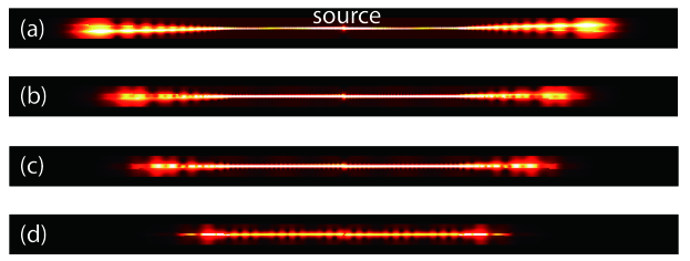
We perform the full wave simulations in loss condition with v=0.001​ωp𝑣0.001subscriptπœ”π‘v=0.001\omega_{p} by using commercial software COMSOL and Fig. 4 shows the electric field distributions in four different operating frequencies, i.e., (a) Ο‰=0.82​ωpπœ”0.82subscriptπœ”π‘\omega=0.82\omega_{p}, (b) Ο‰=0.85​ωpπœ”0.85subscriptπœ”π‘\omega=0.85\omega_{p}, (c) Ο‰=0.88​ωpπœ”0.88subscriptπœ”π‘\omega=0.88\omega_{p} and (d) Ο‰=0.94​ωpπœ”0.94subscriptπœ”π‘\omega=0.94\omega_{p}. As we expected, when we put a magnetic current source in the middle of waveguide, clear double directional rainbow trapping is achieved in the designed waveguide and the electromagnetic (EM) mode with higher working frequency (Ο‰>Ο‰s​p(1)πœ”superscriptsubscriptπœ”π‘ π‘1\omega>\omega_{sp}^{(1)}) will be trapped at thinner Insb position. As shown in Fig .4, one can believe in that this waveguide is capable to trap the EM modes when the frequencies are lied in the frequency band limited by the cutoff frequencies of Edges 1 and 2. Here we emphasis that, even the similar double directional slow light (EM trapping) can be achieved in a all dielectric waveguide, double directional rainbow trapping has never been achieved or reported.

Refer to caption
Figure 3: The schematic of the double directional rainbow trapping structure. The tapered part and straight part have the same length, i.e., L1=L=100​μsubscript𝐿1𝐿100πœ‡L_{1}=L=100\mum. The parameter D of Edge 1 and Edge 2 are D1=(0.03​λp,0.001​λp)subscript𝐷10.03subscriptπœ†π‘0.001subscriptπœ†π‘D_{1}=(0.03\lambda_{p},0.001\lambda_{p}) (the left red point shown in Fig. 2(b)) and D2=(0.016​λp,0.015​λp)subscript𝐷20.016subscriptπœ†π‘0.015subscriptπœ†π‘D_{2}=(0.016\lambda_{p},0.015\lambda_{p}) (the right red point shown in Fig. 2(b)), respectively.
Refer to caption
Figure 4: The electric field distribution of double directional rainbow trapping as (a) Ο‰=0.82​ωpπœ”0.82subscriptπœ”π‘\omega=0.82\omega_{p}, (b) Ο‰=0.85​ωpπœ”0.85subscriptπœ”π‘\omega=0.85\omega_{p}, (c) Ο‰=0.88​ωpπœ”0.88subscriptπœ”π‘\omega=0.88\omega_{p} and (d) Ο‰=0.94​ωpπœ”0.94subscriptπœ”π‘\omega=0.94\omega_{p}. Ο‰πœ”\omega is the working frequency of the magnetic current source. Ο‰c=0.1​ωpsubscriptπœ”π‘0.1subscriptπœ”π‘\omega_{c}=0.1\omega_{p} and Ξ½=0.001​ωp𝜈0.001subscriptπœ”π‘\nu=0.001\omega_{p}.
Refer to caption
Figure 5: (a) EM energy trapping and releasing theory. The red, blue and black lines are respectively the asymptotic frequencies Ο‰s​p(1)superscriptsubscriptπœ”π‘ π‘1\omega_{sp}^{(1)}, Ο‰s​p(2)superscriptsubscriptπœ”π‘ π‘2\omega_{sp}^{(2)} and the cutoff frequency Ο‰c​fsubscriptπœ”π‘π‘“\omega_{cf}. The inset shows the electric field distribution as Ο‰c=0.4​ωpsubscriptπœ”π‘0.4subscriptπœ”π‘\omega_{c}=0.4\omega_{p} with Ο‰=0.94​ωpπœ”0.94subscriptπœ”π‘\omega=0.94\omega_{p}. The waveguide parameter D=(0.03​λp,0.001​λp)𝐷0.03subscriptπœ†π‘0.001subscriptπœ†π‘D=(0.03\lambda_{p},0.001\lambda_{p}). (b) Another double directional rainbow trapping and releasing waveguide. The thickness of the Si layers are constantly being d1=0.02​λpsubscript𝑑10.02subscriptπœ†π‘d_{1}=0.02\lambda_{p} and as shown in Fig. 2(b), the green points represent the parameters D of Edges 1 and 2 of this waveguide, more specifically, D1=(0.02​λp,0.001​λp)subscript𝐷10.02subscriptπœ†π‘0.001subscriptπœ†π‘D_{1}=(0.02\lambda_{p},0.001\lambda_{p}) and D2=(0.02​λp,0.015​λp)subscript𝐷20.02subscriptπœ†π‘0.015subscriptπœ†π‘D_{2}=(0.02\lambda_{p},0.015\lambda_{p}). The electric fields distribution in the simulations as Ο‰=0.94​ωpπœ”0.94subscriptπœ”π‘\omega=0.94\omega_{p} with (c) Ο‰c=0.1​ωpsubscriptπœ”π‘0.1subscriptπœ”π‘\omega_{c}=0.1\omega_{p} and (d) Ο‰c=0.4​ωpsubscriptπœ”π‘0.4subscriptπœ”π‘\omega_{c}=0.4\omega_{p}.
Refer to caption
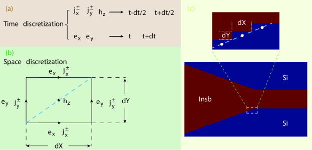
Figure 6: FDTD method in tapered configuration. The (a) time and (b) space discretizations based on Eqs. (4) and (5). (c) A part of the space discretization of the whole waveguide shown in Fig. 3. The blue dashed line shows the Insb-Si interface in real space.
Refer to caption
Figure 7: The electric field distribution in FDTD simulations when (a) t=5​Tp𝑑5subscript𝑇𝑝t=5T_{p} (Tp=2​π/Ο‰psubscript𝑇𝑝2πœ‹subscriptπœ”π‘T_{p}=2\pi/\omega_{p}), (b) t=200​Tp𝑑200subscript𝑇𝑝t=200T_{p}, (c) t=300​Tp𝑑300subscript𝑇𝑝t=300T_{p} and (d) t=1000​Tp𝑑1000subscript𝑇𝑝t=1000T_{p}. We set Ο‰c=0.1​ωpsubscriptπœ”π‘0.1subscriptπœ”π‘\omega_{c}=0.1\omega_{p} (t≀200​Tp𝑑200subscript𝑇𝑝t\leq 200T_{p}) and Ο‰c=0.4​ωpsubscriptπœ”π‘0.4subscriptπœ”π‘\omega_{c}=0.4\omega_{p} (t>200​Tp𝑑200subscript𝑇𝑝t>200T_{p}). The other parameters are the same with Fig. 4(d).

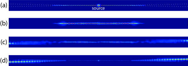
Once we trapped the EM modes, the following question is how to release them. Since the optical properties of the MO materials can be engineered by changing the external magnetic field, in Fig. 5(a), as D=(0.03​λp,0.001​λp)𝐷0.03subscriptπœ†π‘0.001subscriptπœ†π‘D=(0.03\lambda_{p},0.001\lambda_{p}), we plot the asymptotic frequencies and cutoff frequency Ο‰c​fsubscriptπœ”π‘π‘“\omega_{cf} as functions of Ο‰csubscriptπœ”π‘\omega_{c} which has linear relation with the external magnetic field. The green and yellow shaded zones represent Ο‰sp(1)<Ο‰<Ο‰c​fsuperscriptsubscriptπœ”sp1πœ”subscriptπœ”π‘π‘“\omega_{\rm sp}^{(1)}<\omega<\omega_{cf} and Ο‰sp(2)<Ο‰<Ο‰sp(1)superscriptsubscriptπœ”sp2πœ”superscriptsubscriptπœ”sp1\omega_{\rm sp}^{(2)}<\omega<\omega_{\rm sp}^{(1)}, and we name them the trapping zone and releasing zone (the AF region), respectively. The left four points corresponding to the four working frequencies in Fig. 4 and they all fall in the trapping zone when Ο‰c=0.1​ωpsubscriptπœ”π‘0.1subscriptπœ”π‘\omega_{c}=0.1\omega_{p}. If we enlarge the external magnetic field and make Ο‰c=0.4​ωpsubscriptπœ”π‘0.4subscriptπœ”π‘\omega_{c}=0.4\omega_{p} (the right four points), all of the four frequencies fall in the AF region, and the SMPs lies in the AF region can always propagate along the Insb-Si interfaces, therefore, |vg|>0subscript𝑣𝑔0|v_{g}|>0 which implies that the SMPs can not be trapped in the waveguide. As an example, we perform the simulation as shown the inset in Fig. 5(a) as Ο‰c=0.4​ωpsubscriptπœ”π‘0.4subscriptπœ”π‘\omega_{c}=0.4\omega_{p} and Ο‰=0.94​ωpπœ”0.94subscriptπœ”π‘\omega=0.94\omega_{p}, and it is quite clear that the SMPs excited by the source propagate to the end surface but rather be trapped. Besides, other waveguides based on our theory, e.g. the one shown in Fig. 5(b) in which the thickness of Si layers are constant (d1=0.02​λpsubscript𝑑10.02subscriptπœ†π‘d_{1}=0.02\lambda_{p}, the horizontal green line in Fig. 2(b)) can also achieve the double directional rainbow trapping (Fig. 5(c), Ο‰c=0.1​ωpsubscriptπœ”π‘0.1subscriptπœ”π‘\omega_{c}=0.1\omega_{p}) (here, we just show one of the rainbow trapping) and releasing (Fig. 5(d), Ο‰c=0.4​ωpsubscriptπœ”π‘0.4subscriptπœ”π‘\omega_{c}=0.4\omega_{p}) as Ο‰=0.94​ωpπœ”0.94subscriptπœ”π‘\omega=0.94\omega_{p}.

To clearly show the process of trapping and releasing the EM energy, we use the FDTD method re-perform the simulations. For the semiconductor, combing Eq. (1) and Maxwell’s equations, we can obtain

βˆ‚jxΒ±βˆ‚t+2​π​(Ξ½Β―βˆ“i​ω¯c)​jxΒ±=2​π2β€‹Ξ΅βˆžβ€‹ex,superscriptsubscript𝑗π‘₯plus-or-minus𝑑2πœ‹minus-or-plusΒ―πœˆπ‘–subscriptΒ―πœ”π‘superscriptsubscript𝑗π‘₯plus-or-minus2superscriptπœ‹2subscriptπœ€subscript𝑒π‘₯\frac{\partial j_{x}^{\pm}}{\partial t}+2\pi(\overline{\nu}\mp i\overline{\omega}_{c})j_{x}^{\pm}=2\pi^{2}\varepsilon_{\infty}e_{x}, (4a)
βˆ‚jyΒ±βˆ‚t+2​π​(Ξ½Β―βˆ“i​ω¯c)​jyΒ±=2​π2β€‹Ξ΅βˆžβ€‹ey,superscriptsubscript𝑗𝑦plus-or-minus𝑑2πœ‹minus-or-plusΒ―πœˆπ‘–subscriptΒ―πœ”π‘superscriptsubscript𝑗𝑦plus-or-minus2superscriptπœ‹2subscriptπœ€subscript𝑒𝑦\frac{\partial j_{y}^{\pm}}{\partial t}+2\pi(\overline{\nu}\mp i\overline{\omega}_{c})j_{y}^{\pm}=2\pi^{2}\varepsilon_{\infty}e_{y}, (4b)
βˆ‚hzβˆ‚Y=Ξ΅βˆžβ€‹βˆ‚exβˆ‚t+(jx++jxβˆ’)βˆ’i​(jy+βˆ’jyβˆ’),subscriptβ„Žπ‘§π‘Œsubscriptπœ€subscript𝑒π‘₯𝑑superscriptsubscript𝑗π‘₯superscriptsubscript𝑗π‘₯𝑖superscriptsubscript𝑗𝑦superscriptsubscript𝑗𝑦\frac{\partial h_{z}}{\partial Y}=\varepsilon_{\infty}\frac{\partial e_{x}}{\partial t}+(j_{x}^{+}+j_{x}^{-})-i(j_{y}^{+}-j_{y}^{-}), (4c)
βˆ’βˆ‚hzβˆ‚X=Ξ΅βˆžβ€‹βˆ‚eyβˆ‚t+(jy++jyβˆ’)+i​(jx+βˆ’jxβˆ’),subscriptβ„Žπ‘§π‘‹subscriptπœ€subscript𝑒𝑦𝑑superscriptsubscript𝑗𝑦superscriptsubscript𝑗𝑦𝑖superscriptsubscript𝑗π‘₯superscriptsubscript𝑗π‘₯-\frac{\partial h_{z}}{\partial X}=\varepsilon_{\infty}\frac{\partial e_{y}}{\partial t}+(j_{y}^{+}+j_{y}^{-})+i(j_{x}^{+}-j_{x}^{-}), (4d)
βˆ‚eyβˆ‚Xβˆ’βˆ‚exβˆ‚Y=βˆ’βˆ‚h​zβˆ‚t,subscript𝑒𝑦𝑋subscript𝑒π‘₯π‘Œβ„Žπ‘§π‘‘\frac{\partial e_{y}}{\partial X}-\frac{\partial e_{x}}{\partial Y}=-\frac{\partial hz}{\partial t}, (4e)

where ω¯c=Ο‰c/Ο‰psubscriptΒ―πœ”π‘subscriptπœ”π‘subscriptπœ”π‘\overline{\omega}_{c}=\omega_{c}/\omega_{p}, jxsubscript𝑗π‘₯j_{x} and jysubscript𝑗𝑦j_{y} are the induced current components. (ex,ey,hzsubscript𝑒π‘₯subscript𝑒𝑦subscriptβ„Žπ‘§e_{x},e_{y},h_{z}) are the normalized electric field and magnetic field. For the Si layer, we can easily get the similar equations from Eqs. (4c,4d,4e) by setting jxΒ±=0superscriptsubscript𝑗π‘₯plus-or-minus0j_{x}^{\pm}=0, jyΒ±=0superscriptsubscript𝑗𝑦plus-or-minus0j_{y}^{\pm}=0 and letting Ξ΅rsubscriptπœ€π‘Ÿ\varepsilon_{r} replace Ρ∞subscriptπœ€\varepsilon_{\infty}. Then, for the Si layer, we have

βˆ‚hzβˆ‚Y=Ξ΅rβ€‹βˆ‚exβˆ‚t,subscriptβ„Žπ‘§π‘Œsubscriptπœ€π‘Ÿsubscript𝑒π‘₯𝑑\frac{\partial h_{z}}{\partial Y}=\varepsilon_{r}\frac{\partial e_{x}}{\partial t}, (5a)
βˆ’βˆ‚hzβˆ‚X=Ξ΅rβ€‹βˆ‚eyβˆ‚t,subscriptβ„Žπ‘§π‘‹subscriptπœ€π‘Ÿsubscript𝑒𝑦𝑑-\frac{\partial h_{z}}{\partial X}=\varepsilon_{r}\frac{\partial e_{y}}{\partial t}, (5b)
βˆ‚eyβˆ‚Xβˆ’βˆ‚exβˆ‚Y=βˆ’βˆ‚h​zβˆ‚t,subscript𝑒𝑦𝑋subscript𝑒π‘₯π‘Œβ„Žπ‘§π‘‘\frac{\partial e_{y}}{\partial X}-\frac{\partial e_{x}}{\partial Y}=-\frac{\partial hz}{\partial t}, (5c)

Based on Eqs. (4) and (5), we can discrete (ex,ey,hz,jxΒ±,jyΒ±subscript𝑒π‘₯subscript𝑒𝑦subscriptβ„Žπ‘§superscriptsubscript𝑗π‘₯plus-or-minussuperscriptsubscript𝑗𝑦plus-or-minuse_{x},e_{y},h_{z},j_{x}^{\pm},j_{y}^{\pm}) in time domain and space domain as shown in Figs. 6(a,b). One of challenges in applying the FDTD method in such tapered structure is how to define the boundary conditions especially on the tapered Insb-YIG interfaces. Here, we design zig-zag interfaces (see the inset in Fig. 6(c)) instead of the original smooth interfaces (the blue dashed lines in Fig. 6) in real space. We note that around the zig-zag interfaces, if we set suitable ratio d​X/d​Yπ‘‘π‘‹π‘‘π‘ŒdX/dY and let the hzsubscriptβ„Žπ‘§h_{z} of all the units (the white points (hzsubscriptβ„Žπ‘§h_{z}) in Fig. 6(c)) that through the original interface lie on the original interface, the boundary condition is the same with the one in real space, i.e. hzsubscriptβ„Žπ‘§h_{z} is continuous on the Insb-Si interfaces. Therefore, as shown in Fig. 6(c), we design the space discretization for structure shown in Fig. 3 (here, we only show the straight-tapered joint part of the structure). Based on the Eq. (4), Eq. (5) and the time-space discretizations shown in Fig. 6, we perform the FDTD simulations in Fig. 7. Fig. 7(a), (b), (c) and (d) show the electric field distributions when t=5​Tp𝑑5subscript𝑇𝑝t=5T_{p} (Tp=2​π/Ο‰psubscript𝑇𝑝2πœ‹subscriptπœ”π‘T_{p}=2\pi/\omega_{p}), t=200​Tp𝑑200subscript𝑇𝑝t=200T_{p}, t=300​Tp𝑑300subscript𝑇𝑝t=300T_{p} and t=1000​Tp𝑑1000subscript𝑇𝑝t=1000T_{p}, respectively. Note that we set Ο‰c=0.1​ωpsubscriptπœ”π‘0.1subscriptπœ”π‘\omega_{c}=0.1\omega_{p} for t<=200​Tp𝑑200subscript𝑇𝑝t<=200T_{p} and as shown in Figs. 7(a,b), the EM energy is truly trapped in the waveguide which are perfectly fit with our previous result (Fig. 4(d)) solved in COMSOL. For t>200​Tp𝑑200subscript𝑇𝑝t>200T_{p}, we set Ο‰c=0.4​ωpsubscriptπœ”π‘0.4subscriptπœ”π‘\omega_{c}=0.4\omega_{p} and Fig. 7(c) shows that the trapped EM energy is no longer trapped but gradually released. When t=1000​Tp𝑑1000subscript𝑇𝑝t=1000T_{p} the EM energy is mostly localized on the end surfaces which are set to be PEC in these simulations, which is also the same with the result shown in the inset of Fig. 5(a). This kind of rainbow trapping and releasing structure is promising for designing some functional devices and probably can be used to break the time-bandwidth limit (not considered here).

4 Conclusion

In conclusion, we propose a metal-dielectric-semiconductor (under an external magnetic field B0subscript𝐡0B_{0})-dielectric-metal (MDSDM) configuration. In our analysis, we find that slow-light peaks appear in the thin cases (d1Γ—d2<0.001​λpsubscript𝑑1subscript𝑑20.001subscriptπœ†π‘d_{1}\times d_{2}<0.001\lambda_{p}, d1subscript𝑑1d_{1} and d2subscript𝑑2d_{2} are respectively the thicknesses of the semiconductor and the dielectric) and the cutoff frequencies (Ο‰c​fsubscriptπœ”π‘π‘“\omega_{cf}) can change with D=(d1,d2)𝐷subscript𝑑1subscript𝑑2D=(d_{1},d_{2}). Then, we design a tapered, horizontal symmetric waveguide and in the (COMSOL) simulations, the EM modes are trapped in different locations for four different frequencies, i.e. Ο‰=0.82​ωpπœ”0.82subscriptπœ”π‘\omega=0.82\omega_{p}, 0.85​ωp0.85subscriptπœ”π‘0.85\omega_{p}, 0.88​ωp0.88subscriptπœ”π‘0.88\omega_{p} and 0.94​ωp0.94subscriptπœ”π‘0.94\omega_{p} as Ο‰c=0.1​ωpsubscriptπœ”π‘0.1subscriptπœ”π‘\omega_{c}=0.1\omega_{p} (Ο‰c=e​B0/mβˆ—subscriptπœ”π‘π‘’subscript𝐡0superscriptπ‘š\omega_{c}=eB_{0}/m^{*}, where e and mβˆ—superscriptπ‘šm^{*} are, respectively, the charge and effective mass of a electron). More interestingly, when we enlarge the B0subscript𝐡0B_{0} and let Ο‰c=0.4​ωpsubscriptπœ”π‘0.4subscriptπœ”π‘\omega_{c}=0.4\omega_{p}, the trapped energy will be released. We also propose a method to use finite difference time domain(FDTD) method in the designed tapered structure and perform the simulations in time domain, and as a result, clear EM energy trapping and releasing are observed.

Funding information

We acknowledge support by National Natural Science Foundation of China (NSFC) (61372005), National Natural Science Foundation of China (NSFC) under a key project (41331070), and Independent Research Fund Denmark (9041-00333B). The Center for Nanostructured Graphene is sponsored by the Danish National Research Foundation (Project No. DNRF103).

References

  •  1. R.Β E. Prange and S.Β M. Girvin, The Quantum Hall effect (Springer, 1987).
  •  2. F.Β D.Β M. Haldane and S.Β Raghu, ”Possible realization of directional optical waveguides in photonic crystals with broken time-reversal symmetry,” Phys. Rev. Lett. 100(1), 013904 (2008).
  •  3. Z.Β Wang, Y.Β Chong, J.Β D. Joannopoulos, and M.Β SoljačiΔ‡, ”Observation of unidirectional backscattering-immune topological electromagnetic states,” Nature 461(7265), 772 (2009).
  •  4. W. Qiu, Z. Wang, and M.Β SoljačiΔ‡, ”Broadband circulators based on directional coupling of one-way waveguides,” Opt. Express 19(22), 22248-22257 (2011).
  •  5. L. Shen, Y. You, Z. Wang, and X. Deng, ”Backscattering-immune one-way surface magnetoplasmons at terahertz frequencies,” Opt. Express 23(2), 950–962 (2015).
  •  6. D. Jin, L. Lu, Z. Wang, C. Fang, J. D. Joannopoulos, M.Β SoljačiΔ‡, L. Fu, and N. X. Fang, ”Topological magnetoplasmon,” Nat. Commun. 7, 13486 (2016).
  •  7. K. Liu, A. Torki, and S. He, ”One-way surface magnetoplasmon cavity and its application for nonreciprocal devices,” Opt. Lett. 41(4), 800–803 (2016).
  •  8. K. L. Tsakmakidis, A. D. Boardman, and O. Hess, ”’Trapped rainbow’ storage of light in metamaterials,” Nature 450, 397–401 (2007).
  •  9. Y. Su, F. Liu, and Q. Li, ”System performance of slow-light buffering and storage in silicon nano-waveguide,” Proc. SPIE 6783, 67832–67832 (2007).
  •  10. S. W. Su, Y. H. Chen, S. C. Gou, T. L. Horng, and I. A. Yu, ”Dynamics of slow light and light storage in a Doppler-broadened electromagnetically induced-transparency medium: a numerical approach,” Phys. Rev. A 83, 013827 (2011).
  •  11. M.Β SoljačiΔ‡, S. G. Johnson, S. Fan, M. Ibanescu, E. Ippen, and J. D. Joannopoulos, ”Photonic-crystal slow-light enhancement of nonlinear phase sensitivity,” J. Opt. Soc. Am. B 19(9), 2052–2059 (2002).
  •  12. J. E. Heebner, R. W. Boyd, and Q. H. Park, ”Slow light, induced dispersion, enhanced nonlinearity, and optical solitons in a resonator-array waveguide,” Phys. Rev. E-Statistical, Nonlinear Soft Matter. Phys. 65(3), 0366191–0366194 (2002).
  •  13. Y. Chen and S. Blair, ”Nonlinearity enhanced in finite coupled-resonator slow-light waveguides,” Opt. Express 12, 3353–3366 (2004).
  •  14. P. Ku, F. Sedgwick, C. J. Chang-Hasnain, P. Palinginis, T. Li, H. L. Wang, S. W. Chang, and S. L. Chuang, ”Slow light in semiconductor quantum wells,” Opt. Lett. 29, 2291–2293 (2004).
  •  15. B. Wu, J. F. Hulbert, E. J. Lunt, K. Hurd, A. R. Hawkins, and H. Schmidt, ”Slow light on a chip via atomic quantum state control,” Nat. Photonics 4, 776–779 (2010).
  •  16. T. F. Krauss, ”Why do we need slow light?” Nat. Photonics 2(8), 448 (2008).
  •  17. Z. Dutton, M. Budde, C. Slowe, and L. V. Hau, ”Observation of quantum shock waves created with ultra-compressed slow light pulses in a Bose-Einstein condensate,” Science 293(5530), 663–668 (2001).
  •  18. T. Baba, ”Slow light in photonic crystals,” Nat. Photonics 2(8), 465 (2008).
  •  19. T. F. Krauss, ”Slow light in photonic crystal waveguides,” J. Phys. D Appl. Phys. 40(9), 2666 (2007).
  •  20. A. Hosseini, X. Xu, D. N. Kwong, H. Subbaraman, W. Jiang, and R. T. Chen, ”On the role of evanescent modes and group index tapering in slow light photonic crystal waveguide coupling efficiency,” Appl. Phys. Lett. 98(3), 031107 (2011).
  •  21. J.Β Xu, S.Β Xiao, C.Β Wu, H.Β Zhang, X.Β Deng, and L.Β Shen, ”Broadband one-way propagation and rainbow trapping of terahertz radiations,” Opt. Express 27(8), 10659–10669 (2019).
  •  22. L. Shen, J. Xu, Y. You, K. Yuan, and X. Deng, ”One-way electromagnetic mode guided by the mechanism of total internal reflection,” IEEE Photonics Technol. Lett. 30(2), 133–136 (2018).
  •  23. J. J. Brion, R. F. Wallis, A. Hartstein, and E. Burstein, ”Theory of surface magnetoplasmons in semiconductors,” Phys. Rev. Lett. 28(22), 1455–1458 (1972).