Spin-valve Josephson junctions with perpendicular magnetic anisotropy for cryogenic memory
Abstract
We demonstrate a Josephson junction with a weak link containing two ferromagnets, with perpendicular magnetic anisotropy and independent switching fields in which the critical current can be set by the mutual orientation of the two layers. Such pseudospin-valve Josephson junctions are a candidate cryogenic memory in an all superconducting computational scheme. Here, we use Pt/Co/Pt/CoB/Pt as the weak link of the junction with , , and and obtain a change in the critical current for the two magnetization configurations of the pseudospin-valve. Ferromagnets with perpendicular magnetic anisotropy have advantages over magnetization in-plane systems which have been exclusively considered to this point, as in principle the magnetization and magnetic switching of layers in the junction should not affect the in-plane magnetic flux.
Josephson junctions containing ferromagnetic weak links have been of interest over the last twenty years due to the additional physics present when pair correlations from the superconductor (S) interact with the exchange field of the ferromagnet (F) Buzdin (2005); Bergeret, Volkov, and Efetov (2005); Eschrig (2011); Linder and Robinson (2015); Eschrig (2015). Examples include the tuning of the ground state phase difference across a junction from 0 to by changing the thickness of the F layer Buzdin, Bulaevskii, and Panyukov (1982); Ryazanov et al. (2001); Kontos et al. (2002); Robinson et al. (2006). The additional physics can also drive the generation of spin-triplet pair correlations with spin projection along the magnetization axis of the F layer in the junction Bergeret, Volkov, and Efetov (2001a), leading to pair propagation through the F layer over much longer distances than the singlet component Keizer et al. (2006); Khaire et al. (2010); Robinson, Witt, and Blamire (2010); Anwar et al. (2010); Martinez, Pratt, and Birge (2016); Lahabi et al. (2017); Birge (2018).
By adding a second F layer, pseudospin-valve (PSV) Josephson junctions offer functional devices where the ground state phase difference and critical current across the junction can be tuned by controlling the mutual orientations of the F layers Bergeret, Volkov, and Efetov (2001b); Krivoruchko and Koshina (2001); Golubov, Kupriyanov, and Fominov (2002); Barash, Bobkova, and Kopp (2002); Blanter and Hekking (2004); Pajović et al. (2006); Crouzy, Tollis, and Ivanov (2007). One application of these devices is for cryogenic memory, which is needed both to improve energy efficiency of large-scale computation and as part of the effort to interconnect classical computers with quantum computers Holmes, Ripple, and Manheimer (2013); Soloviev et al. (2017); McDermott et al. (2018). The first experimental report by Bell et al. used a Co/Cu/Permalloy PSV to control the critical current of the junction Bell et al. (2004). Promising electrical engineering architectures which integrate the ferromagnetic Josephson junction bits into scalable memory cells compatible with current technology exists, and recently PSV devices have been demonstrated by several groups Bell et al. (2005); Baek et al. (2014); Abd El Qader et al. (2014); Baek et al. (2015); Gingrich et al. (2016); Dayton et al. (2018); Niedzielski et al. (2018); Glick et al. (2018); Madden et al. (2018); Birge, Madden, and Naaman (2018). To date, all experimental works on PSV Josephson junctions have considered in-plane F layers as used by Bell et al..
Here, we construct devices where both F layers have perpendicular magnetic anisotropy (PMA). In order to achieve independent switching of the two F layers, we use the standard approach of having two different materials as ‘hard’ and ‘soft’ magnetic layers, here CoB and Co. Whilst Co has been widely studied in Josephson junctionsRobinson et al. (2006, 2007); Khasawneh, Pratt, and Birge (2009); Satchell and Birge (2018), the amorphous alloy CoB has not previously been used. Both Co/Pt and CoB/Pt interfaces exhibit PMA giving an overall PMA for thin ferromagnetic layers. Previous work using Pt as an interlayer in Co/Ni Josephson junctions found the optimal Josephson current was achieved for Satchell, Loloee, and Birge (2019). Here we use which is adequate to buffer the fcc growth of the Co, generate the PMA and have the Pt act as a spacer to separate the magnetic switching of the layers.
Samples were fabricated into standard “sandwich” planar Josephson junctions using a three stage photolithographic method. First, we defined the bottom electrode stencil in a LOR 7B/S1813 bilayer resist. The [Nb/Au]/Nb bottom electrode, Pt/Co/Pt/CoB/Pt weak link and Nb/Au cap were deposited by dc magnetron sputtering in the Royce Deposition System Roy . The magnetrons were mounted below, and confocal to, the substrate with source-substrate distances of 134 mm. The base pressure of the vacuum chamber was 110. The samples were deposited at room temperature with an Ar (6N purity) gas pressure of 3.610 for the Nb and Au layers and 4.810 for the weak link. The [Nb/Au]/Nb superlattice was used for the base electrode as the superlattice has a lower surface roughness compared to a single Nb layer of comparable total thickness Wang, Pratt, and Birge (2012); Satchell, Loloee, and Birge (2019); Qua .
In the second step, a circular S1813 resist mesa of diameter either 3 or was defined as a mask for broad beam ion milling, which removed the cap and layers comprising the weak link from the bottom electrode except in the area of the junction. The size of the resist mesa mask defines the junction area. This was followed by deposition of SiO insulator by RF sputtering to isolate the bottom electrode.
In the third and final step, the top electrode stencil was defined in S1813 resist, and the top electrode, 150 nm of Nb, was sputter deposited immediately following an in-situ ion mill to ensure a clean interface between the junction mesa and top electrode. The full structure of the final device with thickness in (nm) was [Nb (25)/Au(2.5)]/Nb (20)/Pt (5)/Co (0.6)/Pt (5)/CoB (0.3)/ Pt (5)/Nb (5)/Au (5)/ Nb (150).
After fabrication, devices were measured in a continuous flow cryostat with 3 horizontal superconducting Helmholtz coils. The sample can be rotated between in-plane and out-of-plane applied field. Traditional 4-point-probe transport geometry was used to measure the current-voltage characteristic of the junction with combined Keithley 6221-2182A current source and nano-voltmeter. Magnetization loops of sheet films were measured using a Quantum Design MPMS 3 SQUID magnetometer.
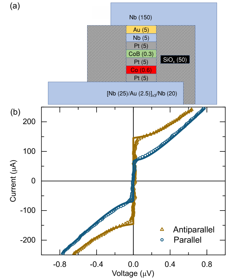
Figure 1 (a) shows the schematic of our final device and the full structure of our multilayer. The Au layers in the structure were sufficiently thin to be heavily proximitized by the adjacent Nb layers. The superconducting electrodes on either side of the weak link were split into separate voltage and current lines. Exemplar I-V curves are shown in Figure 1 (b), which demonstrates the essential function of our device. Measured at a temperature of 1.5 K at zero applied field, the critical current of the junction can be tuned by the relative orientation of the two F layers. The I-V characteristics of our devices follow the standard square-root form, , for as expected for over-damped Josephson junctionsBarone and Paterno (1982) and fits to the data are shown by solid lines in the figure.
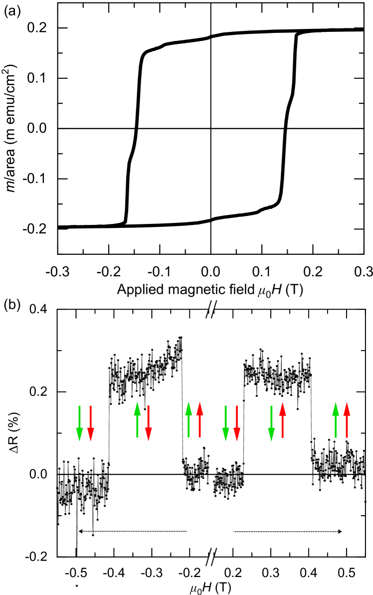
We next report the out-of-plane magnetic switching behaviour of our devices, which must be known and well controlled in order to achieve the two states shown in Figure 1 (b). Figure 2 (a) shows the switching properties of a sheet film sample. The two main magnetic switching events occur close to applied field of . First the Co layer, which has the larger magnetic moment (), switches. Then there is a small plateau in /area where the two layers align antiparallel before the second, thinner, CoB layer switches with the applied field Kikuchi et al. (2011); Metaxas et al. (2010, 2009); Moritz et al. (2004). The small drop in /area close to zero applied field is an artifact from our SQUID and is visible in these data due to the small signals from the thin magnetic layers under study. Dividing the /area by the nominal total thickness of the F layers (0.9 nm) gives a saturation magnetization of about 2190 emu/cm3, which is significantly higher than the saturation magnetization of either bulk Co or CoB. This is due to the additional contribution from polarized Pt in proximity to the F layers Geissler et al. (2001).
| Sample (state) | (V) | (fm2) | (m) | (MAm-2) |
|---|---|---|---|---|
| PSV () | ||||
| PSV () | ||||
| PSV () | ||||
| PSV () | ||||
| Pt-CoB-Pt | ||||
| Pt-Co-Pt |
We perform electrical detection of the magnetic switching in the device structure at the temperature of interest (1.5), Figure 2 (b). Our measurement geometry uses the standard approach for current perpendicular-to-plane magnetoresistance (CPP-MR). An overview of the CPP-MR method, including shortcomings, are given in the review articles Bass and Pratt (1999, 2007); Bass (2016). By using an applied current of we satisfy the condition that the junction is in the normal state (), ensuring true measurement of . R, presented in Figure 2 (b), is the % difference between the out-of-plane magnetic field sweeps in each direction. Due to the giant magnetoresistance effect, when the magnetic layers align antiparallel, a higher resistance state is expected compared to the parallel alignment Baibich et al. (1988). We see this in the device. When the field is applied such that the magnetizations are antiparallel, the resistance of the device is about 0.25% higher than the parallel case. Note that switching behaviour of the devices differ from the sheet films in two key ways. Firstly, the coercive fields of each layer have increased and secondly, the field range in which the device can be aligned antiparallel is much larger. It is known that in PMA thin films, switching occurs by rapid domain wall motion from nucleation sites Kikuchi et al. (2011); Metaxas et al. (2010); Vogel, Moritz, and Fruchart (2006). It is therefore to be expected that the magnetic switching of the patterned junctions occurs at higher applied fields than the sheet films due to the lower probability of a nucleation site in the small junction area.
For practicable memory devices, it will be important to reduce the low temperature switching fields of the ‘free’ magnetic layer, and to remove the requirement for a global applied field by incorporating on-chip switching. Routes towards reducing the coercive fields of the PMA layers include refinement of the ferromagnet thicknesses and exploration of alternative materials. Routes towards on-chip switching of PMA devices include the use of on-chip coils Finizio et al. (2019), which could be made from superconducting material. Spin-orbit torque switching of the barrier state could also be explored Miron et al. (2010); Liu et al. (2012).
For circular Josephson junctions, the (B) response can be described by the Airy function Barone and Paterno (1982),
| (1) |
where is the maximum critical current, is a Bessel function of the first kind, is the flux quantum, and is the flux through the junction,
| (2) |
where , and are the width of the junction, the London penetration depth of the electrodesLon and the total thickness of all the normal metal layers and F layers in the junction. is the applied field and is the amount is shifted from = 0. arises from a combination of an intrinsic contribution due to any in-plane magnetization of the junction, and extrinsic artifacts from trapped flux in the 3 superconducting coil used to perform the measurements. Fits to these equations are shown along with the data on our devices in Figure 3.
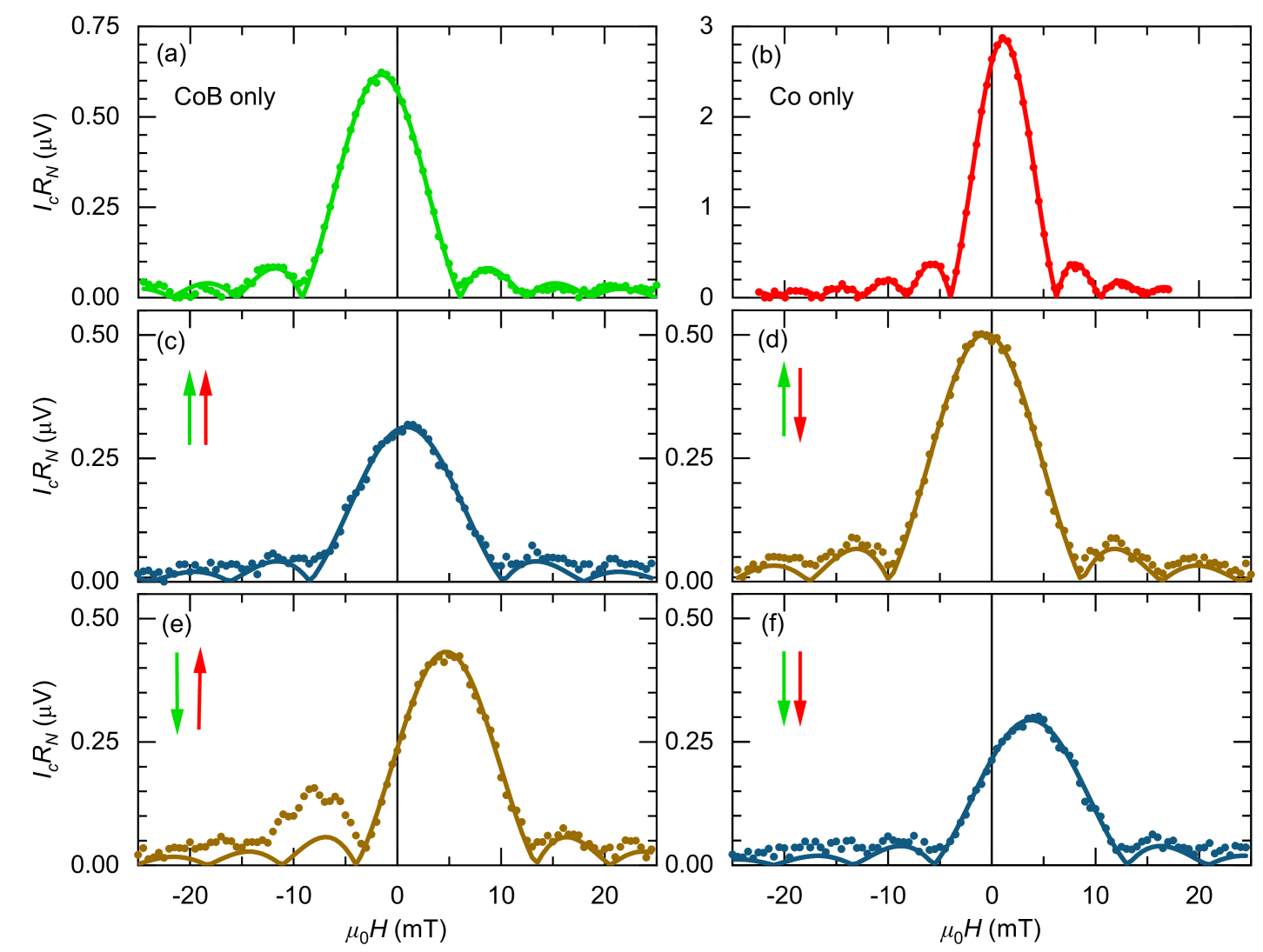
In order to study the contribution to the PSV device from each F layer individually, we fabricated two devices each with only a single F layer and otherwise unaltered structure from that shown in the schematic of Figure 1 (a). The device with Pt(10)/CoB(0.3)/Pt(5) weak link is shown in Figure 3 (a) and with Pt(5)/Co(0.6)/Pt(10) weak link in Figure 3 (b). Prior to these measurements, the junctions were saturated with a 1 out-of-plane applied field at 15 K, to avoid trapping flux vorticies in the superconductor. After the field was set back to 0, the sample was rotated so the measurement field was applied in-plane and then cooled through . The measurements were performed at the base temperature of our cryostat (1.5).
For the single F layer devices, Figure 3 (a,b), (B) is centered close to zero applied field as expected for F layers with PMA. The small in these data suggests there may be either trapped flux in our superconducting coils used to acquire these data or there is a small in-plane component of the magnetization. An in-plane magnetization component can arise either intrinsically or due to magnetization tilting by the applied field. This latter effect, however, cannot account for the , but would cause some distortion to the at larger . Since the single F layer junctions fit well to Eq (1), this tilting effect is minimal. The CoB device is fabricated to a m diameter junction and the Co to m diameter, hence the tighter pattern of the Co. The reported is normalized to the junction area, and thus allows direct comparison despite the different junction sizes. Clearly the Co is much more transparent to supercurrent compared to the CoB, which has a much lower despite being only half as thick. The of the CoB appears to be the limiting factor in the of the PSV, and hence our future research should focus on finding an alternative for the CoB F layer.
In Figure 1 (b) we studied the influence of the layer switching on the critical current at zero applied field. In ferromagnetic Josephson junctions however, the magnetization of the F layer can contribute to the magnetic flux density in the junction, introducing proportional to the magnetization of the F layer collinear with . This can be significant in magnetization in-plane devices, where can be 10’s causing the soft layer to switch prior to reaching in the (B) sweep Niedzielski et al. (2018). In our junctions, where the magnetization of the F layers is perpendicular to plane, we do not expect this to occur as the layers do not contribute significant in-plane magnetization components and cannot be switched by an in-plane applied field. Nonetheless, since there is a small in the junctions with single layers, it is important to measure (B) for each state. These measurements are to confirm that the difference in critical current in Figure 1 (b) is due to the PSV effect and not from any component of magnetization contributing magnetic flux density in the junction.
In Figure 3 (c-f) we study the (B) characteristic of the device with two F layers. To achieve the magnetic state we applied the out-of-plane fields at 15, above . Using the data in Figure 2 (b) as a guide, a saturating field was used for the parallel magnetic alignments. For the antiparallel alignments, the saturating field was followed by a set field of . As per the single layer samples, the field was set back to 0, the sample was rotated, so that the measurement field was applied in-plane, and then cooled to 1.5.
The measurements of (B) confirm that in the parallel alignment the is significantly smaller than in the antiparallel alignment. The maximum value of measured from the two parallel states was V. By contrast, in the antiparallel state the maximum measured was . This corresponds to a . In a memory scheme, the high/low states of the device form a memory bit. By measuring at a constant applied current larger than parallel and less than antiparallel, the device will either be in the superconducting or resistive state. It is also possible that the two states (parallel and antiparallel) correspond to different ground-state phase differences across the junction (0 or ), although our measurements here are not sensitive to such a change. We have summarized our experimental results in Table 1.
In conclusion, we report on pseudospin-valve Josephson junctions with perpendicular magnetic anistropy. The Co layer with thickness and CoB layer with thickness have sufficiently independent switching to allow the device to be placed in either the parallel or antiparallel magnetic configuration. The critical current of the device is strongly dependent on the magnetic configuration, with a (high)low critical current state in the (anti)parallel configuration. This demonstration shows that our work has immediate device application as a memory bit in an all superconducting computation scheme. In the future it will be possible to map a phase diagram for PSV Josephson junctions with perpendicular magnetic anisotropy to allow control of the ground-state phase differences between 0 or , and explore the use of spin-orbit coupling for additional device functionality.
The data associated with this paper are openly available from the University of Leeds data repository Not .
Acknowledgements.
We wish to thank Norman Birge and Reza Loloee for advice and helpful discussions, T. Moorsom, A.J. Huxtable, A. Walton and M. Rogers for experimental assistance. We acknowledge support from the Henry Royce Institute. The work was supported financially through the following EPSRC grants: EP/M000923/1, EP/P022464/1 and EP/R00661X/1. M Algarni acknowledges support from Jeddah University. This project has received funding from the European Unions Horizon 2020 research and innovation programme under the Marie Skłodowska-Curie Grant Agreement No. 743791 (SUPERSPIN).References
- Buzdin (2005) A. I. Buzdin, Rev. Mod. Phys. 77, 935 (2005).
- Bergeret, Volkov, and Efetov (2005) F. S. Bergeret, A. F. Volkov, and K. B. Efetov, Rev. Mod. Phys. 77, 1321 (2005).
- Eschrig (2011) M. Eschrig, Phys. Today 64, 43 (2011).
- Linder and Robinson (2015) J. Linder and J. W. A. Robinson, Nat. Phys. 11, 307 (2015).
- Eschrig (2015) M. Eschrig, Rep. Prog. Phys 78, 104501 (2015).
- Buzdin, Bulaevskii, and Panyukov (1982) A. Buzdin, L. Bulaevskii, and S. Panyukov, JETP Lett 35, 178 (1982).
- Ryazanov et al. (2001) V. V. Ryazanov, V. A. Oboznov, A. Y. Rusanov, A. V. Veretennikov, A. A. Golubov, and J. Aarts, Phys. Rev. Lett. 86, 2427 (2001).
- Kontos et al. (2002) T. Kontos, M. Aprili, J. Lesueur, F. Genêt, B. Stephanidis, and R. Boursier, Phys. Rev. Lett. 89, 137007 (2002).
- Robinson et al. (2006) J. W. A. Robinson, S. Piano, G. Burnell, C. Bell, and M. G. Blamire, Phys. Rev. Lett. 97, 177003 (2006).
- Bergeret, Volkov, and Efetov (2001a) F. S. Bergeret, A. F. Volkov, and K. B. Efetov, Phys. Rev. Lett. 86, 4096 (2001a).
- Keizer et al. (2006) R. Keizer, S. Goennenwein, T. Klapwijk, G. Miao, G. Xiao, and A. Gupta, Nature 439, 825 (2006).
- Khaire et al. (2010) T. S. Khaire, M. A. Khasawneh, W. P. Pratt, and N. O. Birge, Phys. Rev. Lett. 104, 137002 (2010).
- Robinson, Witt, and Blamire (2010) J. W. A. Robinson, J. D. S. Witt, and M. G. Blamire, Science 329, 59 (2010).
- Anwar et al. (2010) M. S. Anwar, F. Czeschka, M. Hesselberth, M. Porcu, and J. Aarts, Phys. Rev. B 82, 100501 (2010).
- Martinez, Pratt, and Birge (2016) W. M. Martinez, W. P. Pratt, and N. O. Birge, Phys. Rev. Lett. 116, 077001 (2016).
- Lahabi et al. (2017) K. Lahabi, M. Amundsen, J. A. Ouassou, E. Beukers, M. Pleijster, J. Linder, P. Alkemade, and J. Aarts, Nat. Commun. 8, 2056 (2017).
- Birge (2018) N. O. Birge, Philos. Trans. Royal Soc. A 376, 20150150 (2018).
- Bergeret, Volkov, and Efetov (2001b) F. S. Bergeret, A. F. Volkov, and K. B. Efetov, Phys. Rev. Lett. 86, 3140 (2001b).
- Krivoruchko and Koshina (2001) V. N. Krivoruchko and E. A. Koshina, Phys. Rev. B 64, 172511 (2001).
- Golubov, Kupriyanov, and Fominov (2002) A. A. Golubov, M. Y. Kupriyanov, and Y. V. Fominov, J. Exp. Theor. Phys 75, 190 (2002).
- Barash, Bobkova, and Kopp (2002) Y. S. Barash, I. V. Bobkova, and T. Kopp, Phys. Rev. B 66, 140503 (2002).
- Blanter and Hekking (2004) Y. M. Blanter and F. W. J. Hekking, Phys. Rev. B 69, 024525 (2004).
- Pajović et al. (2006) Z. Pajović, M. Božović, Z. Radović, J. Cayssol, and A. Buzdin, Phys. Rev. B 74, 184509 (2006).
- Crouzy, Tollis, and Ivanov (2007) B. Crouzy, S. Tollis, and D. A. Ivanov, Phys. Rev. B 75, 054503 (2007).
- Holmes, Ripple, and Manheimer (2013) D. S. Holmes, A. L. Ripple, and M. A. Manheimer, IEEE Trans. Appl. Supercond 23, 1701610 (2013).
- Soloviev et al. (2017) I. I. Soloviev, N. V. Klenov, S. V. Bakurskiy, M. Y. Kupriyanov, A. L. Gudkov, and A. S. Sidorenko, Beilstein J. Nanotechnol 8, 2689 (2017).
- McDermott et al. (2018) R. McDermott, M. Vavilov, B. Plourde, F. Wilhelm, P. Liebermann, O. Mukhanov, and T. Ohki, Quantum Sci. Technol. 3, 024004 (2018).
- Bell et al. (2004) C. Bell, G. Burnell, C. W. Leung, E. J. Tarte, D.-J. Kang, and M. G. Blamire, Appl. Phys. Lett. 84, 1153 (2004).
- Bell et al. (2005) C. Bell, G. Burnell, C.W. Leung, E. J. Tarte, and M. G. Blamire, IEEE Trans. Appl. Supercond 15, 908 (2005).
- Baek et al. (2014) B. Baek, W. H. Rippard, S. P. Benz, S. E. Russek, and P. D. Dresselhaus, Nat. Commun. 5, 3888 (2014).
- Abd El Qader et al. (2014) M. Abd El Qader, R. K. Singh, S. N. Galvin, L. Yu, J. M. Rowell, and N. Newman, Appl. Phys. Lett. 104, 022602 (2014).
- Baek et al. (2015) B. Baek, W. H. Rippard, M. R. Pufall, S. P. Benz, S. E. Russek, H. Rogalla, and P. D. Dresselhaus, Phys. Rev. Applied 3, 011001 (2015).
- Gingrich et al. (2016) E. C. Gingrich, B. M. Niedzielski, J. A. Glick, Y. Wang, D. L. Miller, R. Loloee, W. P. Pratt, and N. O. Birge, Nat. Phys. 12, 564 (2016).
- Dayton et al. (2018) I. Dayton, T. Sage, E. Gingrich, M. Loving, T. Ambrose, N. Siwak, S. Keebaugh, C. Kirby, D. Miller, A. Herr, Q. Herr, and O. Naaman, IEEE Magn. Lett. 9, 3301905 (2018).
- Niedzielski et al. (2018) B. M. Niedzielski, T. J. Bertus, J. A. Glick, R. Loloee, W. P. Pratt, and N. O. Birge, Phys. Rev. B 97, 024517 (2018).
- Glick et al. (2018) J. A. Glick, V. Aguilar, A. B. Gougam, B. M. Niedzielski, E. C. Gingrich, R. Loloee, W. P. Pratt, and N. O. Birge, Sci. Adv. 4, eaat9457 (2018).
- Madden et al. (2018) A. E. Madden, J. C. Willard, R. Loloee, and N. O. Birge, Supercond. Sci. Technol 32, 015001 (2018).
- Birge, Madden, and Naaman (2018) N. O. Birge, A. E. Madden, and O. Naaman, in Spintronics XI, Vol. 10732, edited by H.-J. Drouhin, J.-E. Wegrowe, M. Razeghi, and H. Jaffrès, International Society for Optics and Photonics (SPIE, 2018) pp. 124 – 134.
- Robinson et al. (2007) J. W. A. Robinson, S. Piano, G. Burnell, C. Bell, and M. G. Blamire, Phys. Rev. B 76, 094522 (2007).
- Khasawneh, Pratt, and Birge (2009) M. A. Khasawneh, W. P. Pratt, and N. O. Birge, Phys. Rev. B 80, 020506 (2009).
- Satchell and Birge (2018) N. Satchell and N. O. Birge, Phys. Rev. B 97, 214509 (2018).
- Satchell, Loloee, and Birge (2019) N. Satchell, R. Loloee, and N. O. Birge, Phys. Rev. B 99, 174519 (2019).
- (43) The Royce Deposition System is a multi-chamber, multi-technique thin film deposition tool based at the University of Leeds as part of the Henry Royce Institute.
- Wang, Pratt, and Birge (2012) Y. Wang, W. P. Pratt, and N. O. Birge, Phys. Rev. B 85, 214522 (2012).
- (45) P. Quarterman, N. Satchell, B.J. Kirby, R. Loloee, G. Burnell, N.O. Birge, and J.A. Borchers, In Preparation.
- Barone and Paterno (1982) A. Barone and G. Paterno, Physics and Applications of the Josephson Effect (Wiley, 1982).
- Kikuchi et al. (2011) N. Kikuchi, Y. Suyama, S. Okamoto, and O. Kitakami, J. Appl. Phys 109, 07B904 (2011).
- Metaxas et al. (2010) P. J. Metaxas, R. L. Stamps, J.-P. Jamet, J. Ferré, V. Baltz, B. Rodmacq, and P. Politi, Phys. Rev. Lett. 104, 237206 (2010).
- Metaxas et al. (2009) P. J. Metaxas, P.-J. Zermatten, J.-P. Jamet, J. Ferré, G. Gaudin, B. Rodmacq, A. Schuhl, and R. L. Stamps, Appl. Phys. Lett. 94, 132504 (2009).
- Moritz et al. (2004) J. Moritz, F. Garcia, J. C. Toussaint, B. Dieny, and J. P. Nozières, EPL 65, 123 (2004).
- Geissler et al. (2001) J. Geissler, E. Goering, M. Justen, F. Weigand, G. Schütz, J. Langer, D. Schmitz, H. Maletta, and R. Mattheis, Phys. Rev. B 65, 020405 (2001).
- Bass and Pratt (1999) J. Bass and W. P. Pratt, J. Magn. Magn. Mater 200, 274 (1999).
- Bass and Pratt (2007) J. Bass and W. P. Pratt, J. Phys.: Condens. Matter 19, 183201 (2007).
- Bass (2016) J. Bass, J. Magn. Magn. Mater 408, 244 (2016).
- Baibich et al. (1988) M. N. Baibich, J. M. Broto, A. Fert, F. N. Van Dau, F. Petroff, P. Etienne, G. Creuzet, A. Friederich, and J. Chazelas, Phys. Rev. Lett. 61, 2472 (1988).
- Vogel, Moritz, and Fruchart (2006) J. Vogel, J. Moritz, and O. Fruchart, C R Phys 7, 977 (2006).
- Finizio et al. (2019) S. Finizio, K. Zeissler, S. Wintz, S. Mayr, T. Weßels, A. J. Huxtable, G. Burnell, C. H. Marrows, and J. Raabe, Nano Lett. 19, 7246 (2019).
- Miron et al. (2010) I. M. Miron, G. Gaudin, S. Auffret, B. Rodmacq, A. Schuhl, S. Pizzini, J. Vogel, and P. Gambardella, Nat. Mater. 9, 230 (2010).
- Liu et al. (2012) L. Liu, C.-F. Pai, Y. Li, H. W. Tseng, D. C. Ralph, and R. A. Buhrman, Science 336, 555 (2012).
- (60) Equation 2 in the text is valid when the bottom and top superconducting electrodes have identical London penetration depths and , the thickness of the superconductor. In this case, we must take into account that the bottom electrode is a Nb/Au multilayer ( nmQua ; Madden et al. (2018)) and the top electrode is single layer Nb ( nmFlokstra et al. (2018)). in equation 2 should therefore be replaced by ( + ), where the effective London penetration depth , see reference Barone and Paterno (1982). These considerations are taken into account in our calculations .
- (61) N. Satchell, University of Leeds data repository, 2019, https://doi.org/10.5518/741.
- Flokstra et al. (2018) M. G. Flokstra, R. Stewart, N. Satchell, G. Burnell, H. Luetkens, T. Prokscha, A. Suter, E. Morenzoni, S. Langridge, and S. L. Lee, Phys. Rev. Lett. 120, 247001 (2018).