Comparison between the linear and nonlinear homogenization of graphene and silicon metasurfaces
Abstract
In this paper, we use a versatile homogenization approach to model the linear and nonlinear optical response of two metasurfaces: a plasmonic metasurface consisting of a square array of graphene cruciform patches and a dielectric metasurface consisting of a rectangular array of photonic crystal (PhC) cavities in a silicon PhC slab waveguide. The former metasurface is resonant at wavelengths that are much larger than the graphene elements of the metasurface, whereas the resonance wavelengths of the latter one are comparable to the size of its resonant components. By computing and comparing the effective permittivities and nonlinear susceptibilities of the two metasurfaces, we infer some general principles regarding the conditions under which homogenization methods of metallic and dielectric metasurfaces are valid. In particular, we show that in the case of the graphene metasurface the homogenization method describes very well both its linear and nonlinear optical properties, whereas in the case of the silicon PhC metasurface the homogenization method is less accurate, especially near the optical resonances.
I Introduction
Metamaterials, whose emergence has opened up exciting new opportunities to create novel media with pre-designed physical properties, have been proving to have a significant impact on the development of new approaches and devices for controlling light interaction with matter and achieving key functionalities, including light focusing xkpj16nc ; gzcql10oe ; cz10oe , perfect lensing ss12njp ; gm15prl , perfect absorption nsjd08prl ; sk12prb ; rmcf12oe ; jsns11oe ; sqlf13n , electromagnetic cloaking djbs06s ; ps09mt ; dyygs12nc , imaging with sub-diffraction resolution ag03ieee ; dbcn10oe ; dtem06prl ; zshyycx07oe ; cpl08prl , and optical sensing obt13prl ; apswg09nm ; kymem16nm ; cjxsn13acs . One of the most important functionalities provided by metamaterials is the enhancement of the local optical field igmha13prb ; pegwc11jo ; jwzxs14oe ; zarra08m ; baj09prb ; mdbai14nl ; fzp06nl ; kwb15acsp . This feature is particularly relevant to nonlinear optics since nonlinear optical interactions grow nonlinearly with the applied field. Promising applications of metamaterials can be found in a broad area of science and engineering, including optical filters, sensing and infrastructure monitoring, medical devices, remote aerospace applications, and smart solar power management.
As research in metamaterials advanced, it became clear that the two-dimensional (2D) counterpart of metamaterials, the so-called metasurfaces, would offer the fastest route to functional devices and applications. This is so chiefly because most nanofabrication techniques can conveniently be applied to the planar configuration of metasurfaces. These ultrathin and lightweight optical devices are generally made of sub-wavelength dielectric or metallic elements arranged in one-dimensional (1D) or 2D periodic arrays. Equally important from a practical perspective, the single-layer characteristics of photonic devices based on metasurfaces make them particularly amenable to system integration. Because of their small thickness, light-matter interaction occurs in a reduced volume and as such optical losses in metasurfaces are relatively small. Importantly in nonlinear optics applications, this reduced light propagation distance in metasurfaces means that phase-matching requirements can be relaxed, which greatly reduces the design constraints of nonlinear optical devices based on metasurfaces po07ol ; jmjma15prb ; ad11ome ; cga14prb ; egy16nc ; gst17nrm .
Metasurfaces can mainly be divided into two categories, namely metallic (plasmonic) fllfc16sa ; ya11prb and dielectric metasurfaces yidj14nc ; jimed15acs . Plasmonic metasurfaces, which exploit the resonant excitation of surface plasmons at specific frequencies j15nn ; gja11ome ; kejtn10prl , can greatly enhance the local optical field, but this phenomenon is usually accompanied at optical frequencies by large dissipative losses. Dielectric metasurfaces, on the other hand, experience much smaller optical losses but only provide limited optical field enhancement. Moreover, another difference between the two classes of metasurfaces, which is directly related to the magnitude of the optical losses, is that whereas the resonances in the plasmonic metasurfaces are relatively broad, the (Mie) resonances associated to dielectric metasurfaces are particularly narrow. As a result, dielectric metasurfaces are usually much more dispersive than the plasmonic ones. One effective approach to study metasurfaces is using homogenization methods, which reduce the metasurface to a homogeneous material with specific linear and nonlinear retrieved optical coefficients. These effective physical quantities are determined in such a way that the metasurface and homogenous layer of material have the same optical response.
In this paper, we propose a homogenization method and investigate its accuracy when applied to plasmonic and dielectric metasurfaces. As plasmonic metasurface we consider a graphene metasurface fdf11nl ; smt12nm ; zkfs15sr consisting of a square array of free-standing graphene cruciform patches, whereas the dielectric metasurface is made of a rectangular array of photonic crystal (PhC) cavities possessing high- optical modes, embedded in a silicon PhC slab waveguide. The rationale for our choice is that the two metasurfaces capture the general characteristics of the two main classes of metasurfaces, i.e. plasmonic and dielectric metasurfaces. In particular, the cruciform graphene patches possess strong plasmon resonances characterized by highly confined, enhanced optical near-field. As optical nonlinearity, we consider second-harmonic generation (SHG) by the nonlocal nonlinear polarization, as symmetry considerations imply that the SHG by the the local nonlinear polarization is zero h91BookCh ; psl18jo . Moreover, the silicon PhC cavities were designed so as to possess two high- optical cavity modes separated by the Raman frequency of silicon, which ensures a strong effective Raman nonlinearity of the metasurface ryp18oe .
The remainder of the paper is organized as follows: In the next section we present the geometrical configurations and material parameters characterizing the two metasurfaces considered in this work. Then, in Sec. III, we introduce the linear and nonlinear homogenization method used to extract the constitutive parameters of the metasurfaces, whereas in Sec. IV we apply our homogenization approach to the two metasurfaces and derive general principles regarding the conditions in which the predictions of the homogenization method are valid. In particular, we extract the linear and nonlinear constitutive parameters of the metasurfaces and then compare the optical response of the metasurfaces with that of their homogenized counterparts. Finally, we conclude our paper by summarizing the main findings of our study and discussing some of their implications to future developments pertaining to metamaterials research.
II Description of the graphene and silicon metasurfaces
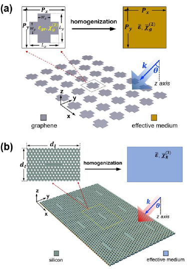
In this section, we describe the geometrical configuration and material parameters of the two metasurfaces investigated in this work, namely the graphene cruciform metasurface illustrated in figure 1(a) and the silicon PhC nanocavity metasurface shown in figure 1(b). In addition, we explain the rationale for our choice of metasurfaces by presenting their main physical properties.
II.1 Geometrical configuration of the graphene and silicon metasurfaces
The graphene metasurface lies in the - plane and consists of a square array of cruciform graphene patches. The symmetry axes of the array coincide with the - and -axes and are oriented along the arms of the crosses, as per figure 1(a). The length and width of the arms of the crosses along the two axes are () and (), respectively, whereas the corresponding periods of the metasurface are and . In this, work, unless otherwise specified, , , and .
The relative electric permittivity of graphene is given by the relation:
| (1) |
where is the thickness of graphene, is the frequency, and the graphene surface conductivity, , is described by the Kubo’s formula gp16book :
| (2) | |||||
Here, , , and are the chemical potential, temperature, and relaxation time, respectively. In this study, we use , , and .
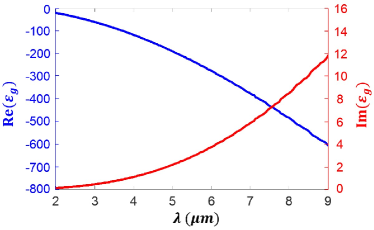
The wavelength dependence of the real and imaginary parts of graphene permittivity, as described by Eq. (1) in conjunction with Eq. (2), are depicted in figure 2. It can be seen in this figure that and , which are spectral characteristics shared by most noble metals.
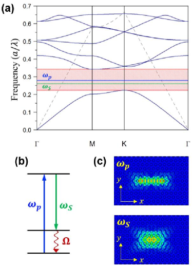
The silicon metasurface, illustrated in figure 1(b), consists of a rectangular array of PhC cavities embedded in a PhC slab waveguide made of silicon () ryp18oe . The PhC slab waveguide comprises a 2D hexagonal lattice of air holes in a silicon slab with the hole radius and slab thickness , where is the lattice constant. Moreover, the optical nanocavities are the so-called PhC cavities, namely they are created by filling in 5 consecutive holes oriented along the symmetry axis of the hexagonal lattice. The periods of the PhC metasurface, defined as the center-to-center distance along the - and -axes between adjacent PhC cavities, are and , respectively. In order to increase the -factor of the optical modes of this PhC nanocavity, we shifted outwardly the end-holes of the cavity by yw05oe .
The PhC cavity is designed in such a way that it possesses two optical modes whose frequencies are separated by the Raman frequency of silicon, th73prb . This ensures a very strong nonlinear coupling between the two optical modes, both because of the large optical field enhancement inside the cavities and also due to favorable spatial overlap between the two optical modes. Consequently, one can achieve an efficient Raman interaction between the two optical modes. This means that the PhC nanocavities can be viewed as artificially engineered, strongly nonlinear “silicon meta-atoms”, which when arranged in some spatial pattern give rise to photonic metasurfaces with large Raman nonlinearity. In particular, if one chooses the lattice constant , the resonance frequency of the pump and Stokes modes are and , respectively, and therefore the condition is fulfilled. Expressed in terms of normalized frequency of , the frequencies of the two optical modes are and . Also, the -factors of the two modes are and . Note that the photonic band structure of the PhC slab and the corresponding cavity modes were computed with RSoft’s BandSOLVE rsoft , with the cavity modes lying in the transverse-magnetic bandgap of the PhC slab waveguide (see figure 3).
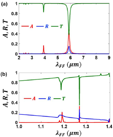
The linear optical response of graphene and silicon metasurfaces is presented in figures 4(a) and 4(b), respectively, and correspond to an -polarized plane wave normally incident onto the metasurface. This figure clearly shows that, in the case of the graphene metasurface, absorption, , reflectance, , and transmittance, , have a series of spectral resonances occurring at common wavelengths. These resonances are due to the generation of localized surface plasmons in the graphene crosses, the resonance wavelength of the fundamental plasmon being . Moreover, it can be seen that the excitation of surface plasmons is accompanied by a large increase of the optical absorption, which suggests that at the corresponding resonance wavelengths the optical near-field is significantly enhanced. Moreover, the spectra of the silicon metasurface show two resonances at the frequencies of the two cavity modes, the width of these resonances being much smaller than that of plasmon resonances.
III Linear and nonlinear homogenization method
In this section, we present first the homogenization approach used to describe the effective optical response of the metasurfaces investigated in this paper and retrieve their effective permittivities and nonlinear susceptibilities and then compare the linear optical response of the original and homogenized metasurfaces so as to clarify the circumstances in which our homogenization approach is accurate.
III.1 Theory of the effective permittivity of metasurfaces
The general linear homogenization method presented here amounts to establishing a relationship between the averaged electric displacement field, D, and the electric field, E, and is known as the field averaging method. It will be expanded later on to the nonlinear case. As it is well known, the constitutive relation of a linear anisotropic material is expressed as , where is the permittivity tensor and the subscripts . The field-average method relies on this relation, the effective permittivity of the medium being defined via a similar relation between the electric field and the electric displacement field:
| (3) | |||||
| (4) |
This method is particularly suitable for describing metasurfaces, because in this case the averaging domain can be naturally defined as the unit cell of the metasurface. Therefore, in the equations above, is the volume of the unit cell of the metasurface.
According to the field averaging method, for an isotropic medium whose permittivity tensor is diagonal, the effective permittivity is evaluated as . This definition can be extended to anisotropic media as follows: First, one defines an auxiliary quantity, , and express the displacement field as , and then calculate the averaged value of each component of the auxiliary quantity:
| (5) |
If we assume that the averaged fields are related by a constitutive relation similar to that corresponding the local fields, namely , and by requiring that the average of the field of the metasurface and the field in the homogenized layer of material are termwise equal, the effective permittivity is determined by the following equation:
| (6) |
This formula has been used to determine the effective permittivity of both metasurfaces. Before moving on to the calculation of the effective nonlinear susceptibilities of the metasurfaces, we note that in the case of the graphene metasurface the volume integrals can be reduced to surface integrals across the midsection of the graphene sheet because the fields across the ultrathin graphene layer vary only slightly.
III.2 Calculation of effective second-order susceptibility of graphene metasurfaces
As we assume that the graphene crosses are free standing, symmetry considerations imply that the dipole (local) nonlinear polarization at the second harmonic (SH) exactly cancels. Consequently, the lowest order SHG is due to the nonlocal nonlinear polarization whose sources are magnetic dipoles and electric quadrupoles oscillating at the SH frequency. It should be noted that if the graphene patches lie onto a substrate the inversion symmetry is broken and consequently the generated SH is due to the dipole nonlinear polarization. The homogenization of such graphene metasurfaces has been recently studied ryp19prb .
This nonlinear polarization and the associated nonlinear surface current in the case of graphene metasurfaces characterized by nonlocal nonlinear polarization can be expressed as h91BookCh :
| (7) | |||
| (8) |
where and are the bulk nonlinear second-order susceptibility and surface nonlinear second-order optical conductivity, respectively, and are related by the following formula:
| (9) |
We stress that instead of a bulk nonlinear susceptibility one can use a surface one, defined as , but we decided to use bulk quantities so that it is more convenient to compare these nonlinear optical coefficients of graphene with those of other centrosymmetric materials.
The surface nonlinear second-order optical susceptibility of graphene has been recently derived in csa16acsn and is given by the following equation:
| (10) |
where the scalar part of the surface second-order conductivity tensor is:
| (11) |
Componentwise, the nonlinear polarization can be evaluated as:
| (12) |
where we introduced a new nonlinear auxiliary quantity defined as . Moreover, the spatial average of this quantity is:
| (13) |
where if r corresponds to a point inside the graphene crosses and if r is in the air region.
If we express the nonlinear polarization in the homogenized metasurface as:
| (14) |
where is the effective nonlinear second-order susceptibility of the homogenized metasurface, and impose the condition that the spatial average of the nonlinear polarization described by Eq. (12) is termwise equal to the polarization in Eq. (14), we obtain the following formula for the effective nonlinear susceptibility:
| (15) |
In this formula and in Eq. (14), the quantity is defined as:
| (16) |
III.3 Theory of effective Raman susceptibility of silicon metasurfaces
The calculation of the effective Ramman susceptibility of the silicon based PhC metasurface described in Sec. 2 is similar to that of the effective second-order susceptibility presented in the preceding subsection, so that here we present only the main steps. A more detailed derivation can be found in ryp18oe .
We start our analysis with the nonlinear Raman polarization at the Stokes frequency, , which can be written as:
| (17) |
where is the Raman susceptibility and and are the optical fields at the pump and Stokes frequencies, respectively. For the sake of simplicity, we assume that the symmetry axes of the array of PhC cavities coincide both with the - and -axes and with the principal axes of silicon. Under these circumstances, the nonzero components of are , with and . The value at resonance of the only independent component is jcd04tap .
We then define the spatially averaged effective Raman polarization:
| (18) |
where the volume integration is taken over the unit cell of the metasurface, together with the effective Raman polarization in a homogenized slab of nonlinear optical medium with the same thickness as that of the PhC slab:
| (19) |
Here, is the effective Raman susceptibility of the homogenized metasurface.
As in the case of the graphene metasurface, we cannot simply impose the condition that the components of the nonlinear polarizations in Eq. (18) and Eq. (19) are equal because in the general case the effective Raman susceptibility tensor, , has 81 independent components, so that the corresponding system of equations is overdetermined. Consequently, we impose the condition that the r.h.s. of equations Eq. (18) and Eq. (19) are termwise identical. Using this constraint, it can be seen that the components of are determined by the following relations:
| (20) |
Note that the components of and cancel for the same set of indices , , , and .
IV Results and Discussions
In this section, we study the circumstances in which our method produces accurate results and use it to understand the main differences between the physical properties of graphene and silicon PhC metasurfaces.
IV.1 Effective permittivities of the graphene and silicon photonic crystal metasurfaces
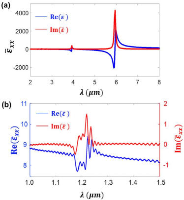
Based on our theoretical analysis, the effective permittivity of the two metasurfaces investigated in this work can be calculated using Eq. (6). The results of our calculations, corresponding to the graphene and silicon PhC metasurfaces, are presented in Fig. 5(a) and Fig. 5(b), respectively. These figures show some similarities between the two spectra but also significant differences. Thus, the effective permittivity of graphene metasurface displays a series of spectral resonances of Lorentzian nature, which occur at the plasmon resonance wavelengths of the graphene crosses. This means that the graphene crosses behave as meta-atoms that possess a series of resonant states, the overall optical response of the metasurface being primarily determined by these resonances. The main reason for this behavior can be traced to the size of the graphene crosses relative to the resonance wavelengths of the plasmons of the graphene crosses. Specifically, since the size of the crosses is much smaller than the plasmon wavelengths, the overall optical response of the graphene metasurface can be viewed as a superposition of the response of weakly interacting Lorentz-type oscillators.
The spectrum of the effective permittivity of the silicon PhC metasurface, on the other hand, presents a series of complex features, which are the result of several phenomena. Thus, the two main resonances of the effective permittivity are due the excitation of the two optical modes of the PhC cavity. The spectral separation between the frequencies of the two cavity modes is relatively small and this leads to interference features in the spectrum of the effective permittivity. The other, weaker spectral peaks are presumably due to leaky modes of the PhC slab.
IV.2 Validation of the homogenization approach
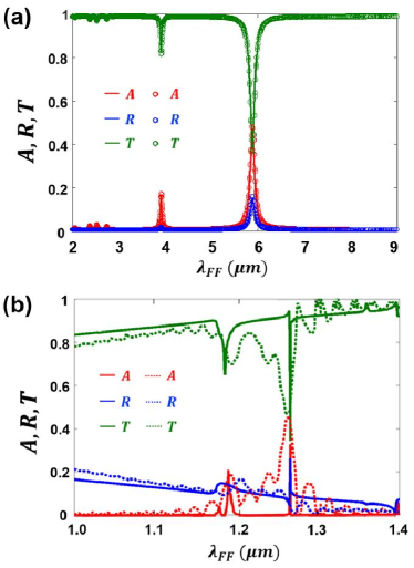
In order to validate the conclusions drawn in the preceding subsection and to investigate the situations in which our homogenization method is accurate, we calculated the absorption, , reflectance, , and transmittance, of both metasurfaces and their homogenized counterparts. The main results of these calculations are summarized in Fig. 6 and they reveal several important ideas. Thus, it can be seen in this figure that in the case of the graphene metasurface the resonances of the transmittance occur at the same wavelengths as the resonances of the effective permittivity, whereas for the silicon PhC metasurface the the two sets of resonances differ to some extent. In order to explain these results, one should note that generally the resonances of the transmittance of a planar optical system correspond to excitation of bound modes of the optical system. In the cases investigated here, the bound modes are localized surface plasmons of graphene crosses for the graphene metasurface and optical modes of the PhC cavities and leaky modes of the PhC slab. Moreover, the excitation of these resonances induces a resonant response of the medium, via the polarization of the medium, which in turn leads to resonances in the spectrum of the effective permittivity of the homogenized metasurfaces.
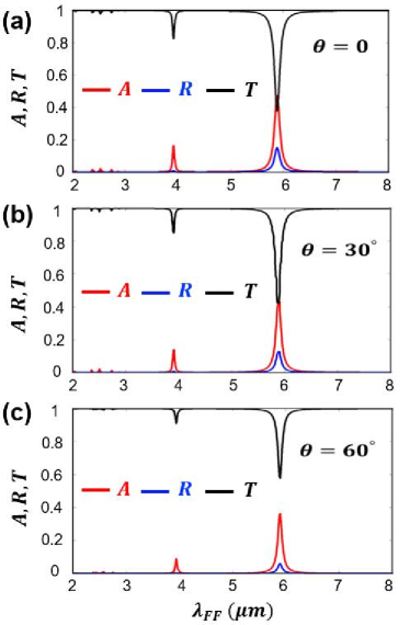
Fig. 6(b) also shows that whereas the linear optical responses of the graphene metasurface and its homogenized counterpart are almost identical, in the case of the silicon PhC metasurface they markedly differ from each other. The main reason for this dichotomy is that the graphene crosses are much smaller than the operating wavelength, which makes them respond to the incident optical field as if they were point-like resonators. By contrast, the size of the PhC cavities is comparable to the resonance wavelength of the cavity modes, which renders our homogenization method to be less accurate in this case. It should also be noted, however, that although the homogenization approach for silicon PhC metasurface cannot provide extremely accurate quantitative values for the effective permittivity, it can still provide us valuable qualitative insights into the governing physics.
These ideas are further illustrated by the dependence of the linear optical response of the graphene metasurface on the angle of incidence, , of the incoming plane wave, which is presented in Fig. 7. Thus, it can be observed that the spectral resonances of the graphene metasurface, calculated for , only slightly varies with , whereas the values of , , and at the resonance wavelengths depend more pronouncedly on . These findings are explained by the fact that the plasmon resonances depend chiefly on the shape of the graphene nano-patches, and thus are independent on , whereas the particular values of , , and depend on the coupling between the incident field and graphene crosses, more specifically on the spatial overlap between the incident wave and the optical field of the graphene plasmons, which is obviously -dependent.
IV.3 Effective second-harmonic susceptibility of graphene metasurfaces
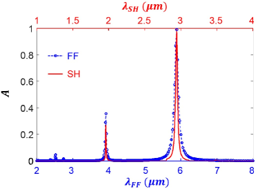
Let us now consider the nonlinear optical properties of the two optical structures and start with the graphene metasurface. The excitation of graphene localized plasmons at the fundamental frequency (FF) induces a strong optical near-field and consequently enhanced nonlinear polarization, which is the source of the generated SH. This phenomenon can be clearly seen in Fig. 8, where we present the absorption spectra at the FF and SH. In particular, it can be observed in this figure that the occurrence of a resonance at the FF is accompanied by a resonance at half of its wavelength in the SH spectrum. For example, the plasmon resonance at the FF of has a correspondent in the SH spectrum at .
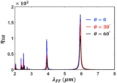
As can be easily inferred from Eq. (9) and Eq. (10), the dominant components (in absolute value) of the second-order susceptibility of graphene are . The value of this component, determined for a FF wavelength , is . Moreover, as a consequence of our approach to the calculation of the effective second-order susceptibility, it is equal to zero for the same set of indices for which the graphene second-order susceptibility is equal to zero. Therefore, in order to quantify the enhancement of the nonlinear optical response of the graphene metasurface, we computed the enhancement factor, , for several values of the angle of incidence, . We summarize the results of these calculations in Fig. 9.
The most important conclusion of this analysis is that, at the wavelength of the fundamental plasmon, the effective second-order susceptibility of the homogenized graphene metasurface is enhanced by almost . More precisely, the maximum achievable enhancement factor is , which means that the maximum value of the effective second-order susceptibility of the homogenized graphene metasurface is . For comparison, the bulk second-order susceptibility of two centrosymmetric materials widely used in nonlinear optics, gold and silicon, are (gold at ) ktr04jap and (silicon at ) fam01ss . Moreover, it can be inferred from Fig. 9 that the enhancement factor is smaller for higher-order plasmons, as in this case the plasmon-induced field enhancement decreases. Another feature revealed by Fig. 9 is that the enhancement factor decreases as the angle of incidence increases, a finding explained by the fact that when increases the spatial overlap between the incident wave and the plasmon mode becomes less favorable and thus the enhancement of the local optical field decreases.
IV.4 Effective Raman susceptibility of the silicon photonic crystal metasurface
Due to the symmetry properties of the silicon PhC metasurface and the orientation of the cavity array with respect to the principal axes of silicon, the only non-zero component of the effective Raman susceptibility of the metasurface is . Therefore, similarly to the case of the graphene metasurface, we define the enhancement factor , where is the dominant component of the Raman susceptibility of silicon. The parameter quantifies the enhancement of the Raman nonlinearity of the silicon PhC metasurface. Moreover, in order to investigate the dependence of the enhancement factor on the angle of incidence, these calculations were performed for .
Following the procedure we just described, we found out that for the values of the incidence angle of , the enhancement factor was , respectively. Thus, it can be seen that a giant enhancement of the effective Raman susceptibility of the silicon PhC metasurface of more than 4 orders of magnitude can be achieved at normal incidence. In order to understand the main reason for this remarkable nonlinearity enhancement, one should note that due to the large -factor of the pump and Stokes cavity modes the field is significantly enhanced as compared to the amplitude of the incident wave, which in conjunction with the fact that the Raman intensity is proportional to the local field to the power of 6, leads to the extremely large resonant enhancement of the Raman response of the silicon PhC metasurface. Moreover, the cavity field enhancement decreases when the angle of incidence increases, due to a weaker coupling between the incoming wave and the cavity modes, which results in reduced nonlinearity enhancement at larger .
As a final remark, it should be noted that the specific design of our metasurface ensures a particularly efficient Raman amplification. To be more specific, let us compare the spectral width of Raman interaction in silicon, opd09aop , with the spectral width of the cavity mode at the Stokes frequency, . Thus, since , an efficient Raman interaction can be achieved.
V Conclusion
In summary, two generic metasurfaces, a graphene metasurface based on graphene cruciform patches and a silicon metasurface with photonic crystal cavities as building blocks, are studied using a versatile and powerful homogenization method. In particular, in order to quantify the linear and nonlinear optical response of the two metasurfaces, we computed their effective permittivities and nonlinear susceptibilities. Our calculations revealed that, in both cases, the nonlinear optical response of the metasurfaces was enhanced by several orders of magnitude at the resonances of the metasurface building blocks. Moreover, by comparing the optical response of the metasurfaces and their homogenized counterparts, we showed that the homogenization approach is more suitable for graphene-based metasurfaces, because in this case the size of the resonant graphene nanostructures is much smaller than the operating wavelength. Even though the homogenization approach for silicon-based metasurfaces appeared to be less accurate, it could still provide valuable qualitative insights into their nonlinear optical response.
It should be noted that our homogenization approach is rather general, in that it can be readily extended to metasurfaces of different configurations or made of optical media with various dispersive and nonlinear optical properties. Moreover, the ideas presented in this paper have broad applicability, as they can be easily extended to other nonlinear optical interactions of practical interest, including third-harmonic generation, four-wave mixing, and sum- and difference frequency generation.
Funding
European Research Council (ERC) (ERC-2014-CoG-648328); China Scholarship Council (CSC) and University College London (UCL) (201506250086).
References
- (1) M. Veysi, C. Guclu, O. Boyraz, and F. Capolino, “Thin anisotropic metasurfaces for simultaneous light focusing and polarization manipulation,” J. Opt. Soc. Am. B 32, 318-323 (2015).
- (2) G. Ren, Z. Lai, C. Wang, Q. Feng, L. Liu, K. Liu, and X. Luo, “Subwavelength focusing of light in the planar anisotropic metamaterials with zone plates,” Opt. Express 18, 18151-18157 (2010).
- (3) C. Ma and Z. Liu, “Focusing light into deep subwavelength using metamaterial immersion lenses,” Opt. Express 18, 4838-4844 (2010).
- (4) S. Maslovski and S. Tretyakov, “Perfect lensing with phase-conjugating surfaces: toward practical realization,” New J. Phys. 14, 035007 (2012).
- (5) G. Rosenblatt and M. Orenstein, “Perfect lensing by a single interface: defying loss and bandwidth limitations of metamaterials,” Phys. Rev. Lett. 115, 195504 (2015).
- (6) N. I. Landy, S. Sajuyigbe, J. J. Mock, D. R. Smith, and W. J. Padilla, “Perfect metamaterial absorber,” Phys. Rev. Lett. 100, 207402 (2008).
- (7) S. Feng and K. Halterman, “Coherent perfect absorption in epsilon-near-zero metamaterials,” Phys. Rev. B 86, 165103 (2012).
- (8) R. Alaee, M. Farhat, C. Rockstuhl, and F. Lederer, “A perfect absorber made of a graphene micro-ribbon metamaterial,” Opt. Express 20, 28017-28024 (2012).
- (9) Y. Jin, S. Xiao, N. A. Mortensen, and S. He, “Arbitrarily thin metamaterial structure for perfect absorption and giant magnification,” Opt. Express 19, 11114-11119 (2011).
- (10) S. Song, Q. Chen, L. Jin, and F. Sun, “Great light absorption enhancement in a graphene photodetector integrated with a metamaterial perfect absorber,” Nanoscale 5, 9615-9619 (2013).
- (11) D. Schurig, J. J. Mock, B. J. Justice, S. A. Cummer, J. B. Pendry, A. F. Starr, and D. R. Smith, “Metamaterial electromagnetic cloak at microwave frequencies,” Science 314, 977-980 (2006).
- (12) P. Alitalo and S. Tretyakov, “Electromagnetic cloaking with metamaterials,” Mater. Today 12, 22-29 (2009).
- (13) D. Shin et al, “Broadband electromagnetic cloaking with smart metamaterials,” Nat. Commun. 3, 1213 (2012).
- (14) C. Luo, S. G. Johnson, J. D. Joannopoulos, and J. B. Pendry, “Subwavelength imaging in photonic crystals,” Phys. Rev. B 68, 045115 (2003).
- (15) S. Foteinopoulou and C. M. Soukoulis, “Electromagnetic wave propagation in two-dimensional photonic crystals: A study of anomalous refractive effects,” Phys. Rev. B 72, 165112 (2005).
- (16) T. Decoopman, G. Tayeb, S. Enoch, D. Maystre, and B. Gralak, “Photonic crystal lens: from negative refraction and negative index to negative permittivity and permeability,” Phys. Rev. Lett. 97, 073905 (2006).
- (17) Z. Liu, S. Durant, H. Lee, Y. Pikus, Y. Xiong, C. Sun, and X. Zhang, “Experimental studies of far-field superlens for sub-diffractional optical imaging,” Opt. Express 15, 6947-6954 (2007).
- (18) R. Chatterjee, N. C. Panoiu, K. Liu, Z. Dios, M. B. Yu, M. T. Doan, L. J. Kaufman, R. M. Osgood, and C. W. Wong, “Achieving Subdiffraction Imaging through Bound Surface States in Negative Refraction Photonic Crystals in the Near-Infrared Range,” Phys. Rev. Lett. 100, 187401 (2008).
- (19) E. J. Osley, C. G. Biris, P. G. Thompson, R. R. F. Jahromi, P. A. Warburton, and N. C. Panoiu, “Fano Resonance Resulting from a Tunable Interaction between Molecular Vibrational Modes and a Double Continuum of a Plasmonic Metamolecule,” Phys. Rev. Lett. 110, 087402 (2013).
- (20) A. V. Kabashin, P. Evans, S. Pastkovsky, W. Hendren, G. A. Wurtz, R. Atkinson, R. Pollard, V. A. Podolskiy, and A. V. Zayats, “Plasmonic nanorod metamaterials for biosensing,” Nat. Mater. 8, 867 (2009).
- (21) K. V. Sreekanth, Y. Alapan, M. ElKabbash, E. Ilker, M. Hinczewski, U. A. Gurkan, A. De Luca, and G. Strang, “Extreme sensitivity biosensing platform based on hyperbolic metamaterials,” Nat. Mater. 15, 621 (2016).
- (22) C. Cao et al, “Metamaterials-based label-free nanosensor for conformation and affinity biosensing,” ACS Nano 7, 7583-7591 (2013).
- (23) I. Al-Naib et al, “Effect of local field enhancement on the nonlinear terahertz response of a silicon-based metamaterial,” Phys. Rev. B 88, 195203 (2013).
- (24) P. Ding, E. Liang, G. Cai, W. Hu, C. Fan, and Q. Xue, “Dual-band perfect absorption and field enhancement by interaction between localized and propagating surface plasmons in optical metamaterials,” J. Opt. 13, 075005 (2011).
- (25) J. Zhang, W. Liu, Z. Zhu, X. Yuan, and S. Qin, “Strong field enhancement and light-matter interactions with all-dielectric metamaterials based on split bar resonators,” Opt. Express 22, 30889-30898 (2014).
- (26) Z. Liu, A. Boltasseva, R. H. Pedersen, R. Bakker, A. V. Kildishev, V. P. Drachev, and V. M. Shalaev, “Plasmonic nanoantenna arrays for the visible,” Metamaterials 2, 45-51 (2008).
- (27) B. Kante, A. de Lustrac, and J. M. Lourtioz, “In-plane coupling and field enhancement in infrared metamaterial surfaces,” Phys. Rev. B 80, 035108 (2009).
- (28) M. R. Shcherbakov et al, “Enhanced third-harmonic generation in silicon nanoparticles driven by magnetic response,” Nano Lett. 14, 6488-6492 (2014).
- (29) W. Fan, S. Zhang, N. C. Panoiu, A. Abdenour, S. Krishna, R. M. Osgood, K. J. Malloy, and S. R. J. Brueck, “Second Harmonic Generation from a Nanopatterned Isotropic Nonlinear Material,” Nano Lett. 6, 1027-1030 (2006).
- (30) S. Kruk, M. Weismann, A. Y. Bykov, E. A. Mamonov, I. A. Kolmychek, T. Murzina, N. C. Panoiu, D. N. Neshev, and Y. S. Kivshar, “Enhanced Magnetic Second-Harmonic Generation from Resonant Metasurfaces,” ACS Photon. 2, 1007-1012 (2015).
- (31) N. C. Panoiu and R. M. Osgood, “Enhanced optical absorption for photovoltaics via excitation of waveguide and plasmon-polariton modes,” Opt. Lett. 32, 2825-2827 (2007).
- (32) J. S. Gomez-Diaz, M. Tymchenko, J. Lee, M. A. Belkin, and A. Alu, “Nonlinear processes in multi-quantum-well plasmonic metasurfaces: electromagnetic response, saturation effects, limits, and potentials,” Phys. Rev. B 92, 125429 (2015).
- (33) A. Rose and D. R. Smith, “Overcoming phase mismatch in nonlinear metamaterials,” Opt. Mater. Express 1, 1232-1243 (2011).
- (34) C. Argyropoulos, G. D. Aguanno, and A. Alu, “Giant second-harmonic generation efficiency and ideal phase matching with a double e-near-zero cross-slit metamaterial,” Phys. Rev. B 89, 235401 (2014).
- (35) E. Almeida, G. Shalem, and Y. Prior, “Subwavelength nonlinear phase control and anomalous phase matching in plasmonic metasurfaces,” Nat. Commun. 7, 10367 (2016).
- (36) G. Li, S. Zhang, and T. Zentgraf, “Nonlinear photonic metasurfaces,” Nat. Rev. Mater. 2, 17010 (2017).
- (37) F. Qin et al, “Hybrid bilayer plasmonic metasurface efficiently manipulates visible light,” Sci. Adv. 2, e1501168 (2016).
- (38) Y. Zhao and A. Alu, “Manipulating light polarization with ultrathin plasmonic metasurfaces,” Phys. Rev. B 84, 205428 (2011).
- (39) Y. Yang, I. I. Kravchenko, D. P. Briggs, and J. Valentine, “All-dielectric metasurface analogue of electromagnetically induced transparency,” Nat. Commun. 5, 5753 (2014).
- (40) J. Sautter, I. Staude, M. Decker, E. Rusak, D. N. Neshev, I. Brener, and Y. S. Kivshar, “Active tuning of all-dielectric metasurfaces,” ACS Nano 9, 4308-4315 (2015).
- (41) J. B. Khurgin, “How to deal with the loss in plasmonics and metamaterials,” Nat. Nanotechnol. 10 2 (2015).
- (42) G. V. Naik, J. Kim, and A. Boltasseva, “Oxides and nitrides as alternative plasmonic materials in the optical range,” Opt. Mater. Express 1, 1090-1099 (2011).
- (43) K. Tanaka, E. Plum, J. Y. Ou, T. Uchino, and N. I. Zheludev, “Multifold enhancement of quantum dot luminescence in plasmonic metamaterials,” Phys. Rev. Lett. 105, 227403 (2010).
- (44) F. H. Koppens, D. E. Chang, and F. J. Garcia de Abajo, “Graphene plasmonics: a platform for strong light–matter interactions,” Nano Lett. 11, 3370-3377 (2011).
- (45) S. H. Lee et al, “Switching terahertz waves with gate-controlled active graphene metamaterials,” Nat. Mater. 11, 936 (2012).
- (46) Z. Li, K. Yao, F. Xia, S. Shen, J. Tian, and Y. Liu, “Graphene plasmonic metasurfaces to steer infrared light,” Sci. Rep. 5, 12423 (2015).
- (47) T. F. Heinz, “Second-order nonlinear optical effects at surfaces and interfaces. In Modern Problems in Condensed Matter Sciences,” in Nonlinear Surface Electromagnetic Phenomena, H.E. Ponath and G.I. Stegeman, eds. (Amsterdam: Elsevier, 1991), 29, pp. 353-416.
- (48) N. C. Panoiu, W. E. I. Sha, D. Y. Lei, and G. C. Li, “Nonlinear optics in plasmonic nanostructures,” J. Opt. 20, 083001 (2018).
- (49) Q. Ren, J. W. You, and N. C. Panoiu, “Giant enhancement of the effective Raman susceptibility in metasurfaces made of silicon photonic crystal nanocavities,” Opt. Express 26, 30383-30392 (2018).
- (50) P. A. D. Goncalves and N. M. Peres, An introduction to graphene plasmonics (World Scientific, Singapore, 2016).
- (51) X. Yang and C. W. Wong, “Design of photonic band gap nanocavities for stimulated Raman amplification and lasing in monolithic silicon,” Opt. Express 13, 4723-4730 (2005).
- (52) P. A. Temple and C. E. Hathaway, “Multiphonon Raman spectrum of silicon,” Phys. Rev. B 7, 3685 (1973).
- (53) BandSOLVETM, https://www.synopsys.com.
- (54) Q. Ren, J. W. You, and N. C. Panoiu, “Large enhancement of the effective second-order nonlinearity in graphene metasurfaces,” Phys. Rev. B 99, 205404 (2019).
- (55) J. D. Cox, I. Silveiro, and F. J. Garcia de Abajo, “Quantum effects in the nonlinear response of graphene plasmons,” ACS Nano 10, 1995-2003 (2016).
- (56) B. Jalali and S. Fathpour, “Silicon photonics,” J. Lightwave Technol. 24, 4600-4615 (2006).
- (57) D. Krause, C. W. Teplin, and C. T. Rogers, “Optical surface second harmonic measurements of isotropic thin-film metals: Gold, silver, copper, aluminum, and tantalum,” J. Appl. Phys. 96, 3626-3634 (2004).
- (58) M. Falasconi, L. C. Andreani, A. M. Malvezzi, M. Patrini, V. Mulloni, and L. Pavesi, “Bulk and surface contributions to second-order susceptibility in crystalline and porous silicon by second-harmonic generation,” Surf. Sci. 481, 105-112 (2001).
- (59) R. M. Osgood, N. C. Panoiu, J. I. Dadap, X. Liu, X. Chen, I. W. Hsieh, E. Dulkeith, W. M. J. Green, and Y. A. Vlasov, “Engineering nonlinearities in nanoscale optical systems: physics and applications in dispersion-engineered silicon nanophotonic wires,” Adv. Opt. Photon. 1, 162-235 (2009).