\carlitoPoisson_CCD: A dedicated simulator for modeling CCDs
Abstract
Keywords:
LSST, modeling, camera, CCD, simulation, diffusion, image processing.
A dedicated simulator, \carlitoPoisson_CCD, has been constructed which models astronomical CCDs by solving Poisson’s equation numerically and simulating charge transport within the CCD. The potentials and free carrier densities within the CCD are self-consistently solved for, giving realistic results for the charge distribution within the CCD storage wells. The simulator has been used to model the CCDs which are being used to construct the LSST digital camera. The simulator output has been validated by comparing its predictions with several different types of CCD measurements, including astrometric shifts, brighter-fatter induced pixel-pixel covariances, saturation effects, and diffusion spreading. The code is open source and freely available.
1 Introduction
Charge Coupled Devices (CCDs) have been the workhorse devices for astronomical imaging for some time. George Smith’s Nobel lecture at [1] gives an excellent summary of the early history. While other detectors are making inroads, CCDs are still the dominant imaging device in astronomical applications. In recent years thick, fully depleted CCDs with their wide spectral response have been applied to spectroscopic applications as well as imaging. Although these devices have high quantum efficiency, relatively good linearity, and acceptable dynamic range, they have a number of problematic effects that can impact the precision and accuracy of astronomical data. It is important that these effects are well understood so that they can be accounted for during image processing. To help understand these effects, we have built a dedicated simulator, \carlitoPoisson_CCD, which solves the electrostatics in the bulk silicon of the CCD, and propagates incoming charges down to the collecting wells where they are collected and stored. The simulator has proven very useful for understanding a number of CCD effects, which will be described in this paper.
Of course, detailed semiconductor modeling codes already exist, are commercially available, and have been validated against silicon results. What is the purpose of developing yet another simulator? The answer is severalfold. First, commercial semiconductor codes typically use proprietary source codes and are quite expensive, while the code described here is open source and freely available [2]. Second, using a commercial semiconductor device simulator requires spending quite a bit of time learning to use the code and set up the initial conditions. The code described here sets up the initial conditions for a typical CCD with a few simple configuration parameters. A third reason is that some of the commercial tools have trouble handling grids physically large enough to simulate a meaningful number of pixels. This code circumvents this by using a variable grid spacing, as described in Section 2.1. Also, it is hoped that this code is simple enough that it can be mastered by people who are not semiconductor experts. The target user group is people in the astronomy field who want to answer questions about CCDs without investing a great deal of time learning the details of semiconductor physics.
The code was developed as part of the development effort of the LSST. The LSST, originally known as the Large Synoptic Survey Telescope, is now known as the Simonyi Survey Telescope at the Vera Rubin Observatory, and will be used to conduct a ten-year survey of the southern sky known as the Legacy Survey of Space and Time. This instrument is an innovative, large, fast survey facility currently under construction at Cerro Pachon in Chile [3]. The digital camera, also currently under construction, consists of approximately 3.2 gigapixels and is the largest digital camera ever constructed. The camera uses fully-depleted silicon CCDs which are back illuminated and 100 microns thick in order to optimize quantum efficiency in the near infrared. The imaging area consists of 189 CCDs, with each CCD containing 16 imaging regions laid out in an 8x2 array. Each imaging region has a pixel array with approximately 500x2000 10 micron square pixels, giving 16 Megapixels total. Each imaging region also has its own independent amplifier ([4], [5]). The focal plane contains CCDs from two different vendors, the ITL STA3800C from the University of Arizona Imaging Technology Laboratory [6], and the E2V CCD250 from Teledyne E2V [7]. However, although this code was developed and tested against these two CCDs from the LSST project, it has already found more general use on other CCDs ([8]), and the hope is that this will continue.
This paper is divided into several sections. In Section 2, we give an overview of the simulator, describing the basic structure of the simulation volume, how we solve the semiconductor equations, and how we treat incoming photons. We also show a number of examples of the outputs available from the simulator. In Section 3, we review a number of the validation tests that were performed to validate the simulation results against measured data of different kinds, and finally we conclude.
2 Overview
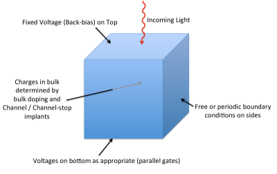
The simulator performs two basic tasks, as shown in Figure 1. First, given the charges in the silicon bulk and the boundary conditions determined by potentials applied to the silicon surface, the simulator solves Poisson’s equation numerically to determine the potentials and electric fields in the silicon bulk. The solution to Poisson’s equation is determined using the technique of successive over-relaxation (SOR - see for example [9]), and using multi-grid methods (see Section 2.4) to speed convergence. In regions where there are mobile carriers (holes and electrons) quasi-Fermi level methods are used to simultaneously solve for the potentials and free carrier densities in the device. The electric fields are determined by numerically differentiating the electrostatic potential. In general, the simulator only solves for the potentials and free-carrier densities in equilibrium, and is not intended to give transient solutions. However, it is possible to repeatedly solve the equations with slight changes in initial conditions in order to give transient results. This technique has been used to generate movies of the CCD charge transport, as discussed in Section 3.6.
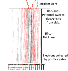
After solving for the device potentials, the second major task of the simulator comes into play. As incoming photons enter the CCD, they generate hole-electron pairs. The electric field in the CCD separates these charges, and the electrons propagate down to the collecting wells where they are collected, stored, and later counted. The simulator models this carrier transport in a physically realistic way, in order to determine in which pixel a generated carrier ends up. This is very useful for modeling pixel distortions that result from electric fields in the device, either built-in electric fields, such as those due to “tree rings”[10], or electric fields due to collected charges, such as those that lead to the brighter-fatter (BF) effect ([11], [12], [13], [14], [15]). Note that in an astronomical CCD, the time between incoming charges (on the order of msec) is typically much longer than the time required for a charge to propagate down to the bottom (on the order of nsec). Also, a single charge has little impact on the existing potentials and fields. So it is an excellent approximation to assume that a single charge propagates in a frozen electric field. The simulator is designed so that if multiple charges are being added, the user can choose how often to re-solve Poisson’s equation. A comment here about the nature of the charges is in order. The simulator is designed for N-channel CCDs (with P-type substrate), where the collected charges are electrons, and for the rest of the paper we will make that assumption. There is no physical reason why it will not work for P-channel CCDs (with N-type substrate), but it is not currently designed to support them. Most of the work in adapting it for P-channel CCDs would be nomenclature related, basically interchanging the names of holes and electrons, but adjustment of parameters like mobilities and effective masses would also be needed. This could be done if there is demand for it.
2.1 Basic structure of the simulations
The simulator is written in C++, and is controlled by a text-based configuration file, which contains all of the information about the silicon volume, pixel sizes, number of pixels, any non-pixel regions, etc. The configuration file also defines the problem being solved. By convention the configuration file has a .cfg extension, but this is not necessary. Appendix A lists the configuration parameters. As the simulation progresses, it writes out a number of files. Large files containing information like potentials, charge densities, electric fields at each grid point are written as high-density HDF5 files, having file extension .hdf5. Several smaller text files, with a .dat extension, are written which contain information on the grids or the number of electrons in each pixel. After the simulation has completed, easily modifiable Python scripts are used to plot out results as desired.
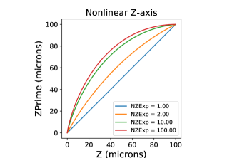
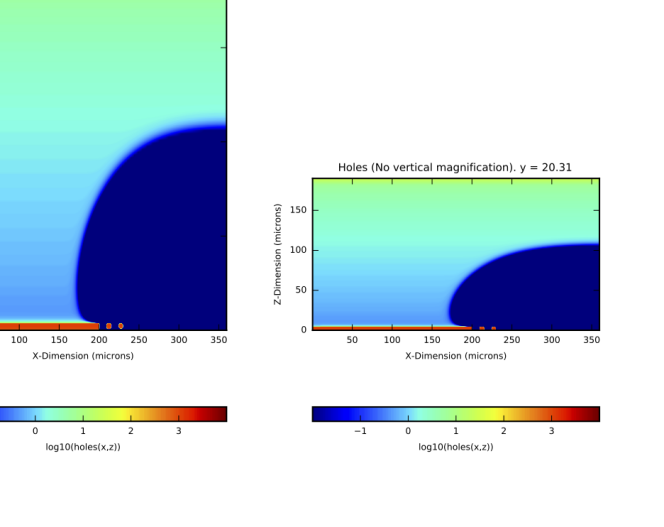
The simulation volume is set up on a fixed three-dimensional rectangular grid, which does not change once the simulation has started. One begins by deciding the number of grid cells in each dimension. Because multi-grid methods are used (see Section 2.4), the number of grid cells in each dimension must be a multiple of 32. Note that as a convention, we refer to the side of the CCD where the circuitry is patterned as the bottom, and the side where the incident light comes in as the top. For the LSST CCDs, which are 100 microns thick and have pixels 10 microns square, a typical resolution is to have 32 simulation grid cells per pixel, so that each grid cell is 0.31 microns. Initially, the grid was defined to be completely uniform in all three dimensions. However, for thick CCDs like those used in the LSST, the potentials and fields change rapidly in the region near the bottom, and only very slowly near the top. When the simulation had enough resolution to be accurate in the rapidly changing region at the bottom, most grid cells were wasted near the top. Of course, adaptive grid methods solve this problem, but also make the code much more complex, which defeated the purpose of having a relatively simple simulator. The solution chosen in this work was to use a non-linear grid in the Z-dimension only. This has proven to give high resolution where needed, without adding significant complexity to the simulation code. Figure 2 shows the scheme. This introduces some additional partial derivatives, as discussed more in section 2.3, but these values can be pre-calculated and this is much simpler than an adaptive grid scheme.
2.2 Setting up the initial conditions
Because the simulator is not a general purpose semiconductor solver, and is intended to model devices with a given structure, certain assumptions are made about the structure of the CCD which simplifies building the device structure. This is one of the reasons why this code is so much simpler than a commercial device simulator. It is assumed that the CCD is a slab of silicon with a given thickness given by the parameter “SensorThickness”. It is assumed that the top surface of the CCD is at a fixed voltage given by the parameter “Vbb”. The bottom surface of the CCD has voltages specified by the various gate potentials. The doping deep in the silicon is asumed constant with a value given by “BackgroundDoping”, although a periodic variation in this doping can be introduced using the “TreeRing” parameters. The doping level is assumed to be modified by the introduction of implants from the bottom side. There are several options for these doping profiles, including a square profile of a given depth or a sum of N Gaussian profiles. Use of 1 or 2 Gaussian profiles has been found to accurately reproduce the measured doping profiles on commercial CCDs. For more details on this, see [16].
2.2.1 Pixel arrays
Setting up the initial conditions in the periodic pixel array is straightforward, and is specified by a relatively small number of parameters which describe the gate voltages and doping levels. Rather than go through these in detail, the reader is referred to Appendix A or the “pixel-itl” and “pixel-e2v” examples at [2].
2.2.2 Fixed regions
Setting up the initial conditions in non-periodic regions outside the pixel array is straightforward, but more laborious than setting up the pixel arrays. The extents, dopings, applied voltages, and quasi-Fermi levels need to be specified for each region. At present only rectangular regions are supported. Also, it is assumed that the same doping profiles which are used in the pixel array are used in the surrounding circuitry, so the only options for doping profiles are the channel doping, the channel stop doping, and no doping. Examples of simulations setting up non-periodic regions are the “edge.cfg”, “trans.cfg”, and “io.cfg” files at [2], and the results of these simulations are detailed in Section 3.
2.3 Solving for the potentials, fields, and free carrier densities
In this section we give a brief description of the methods that are used to solve Poisson’s equation on the grid. We are trying to solve the following equation, where is the potential, is the charge density, and is the dielectric constant of silicon:
| (1) |
Each of the partial derivatives can be discretized on a rectangular grid with grid spacing h as follows:
| (2) |
Giving for the discretized Poisson’s equation:
| (3) |
This can be turned into an iterative equation, and basically one just iterates until convergence:
| (4) |
Which we write in shorthand as follows:
| (5) |
where we define:
| (6) |
and we have split into a fixed charge density and a mobile charge density . However, is a highly nonlinear function of the potential , as described below. In quasi-equilibrium, the drift current and the diffusion current are equal, giving a net current of zero, so we can write (see Sze [17], for example):
| (7) |
Here is the electron charge, is the electron mobility, is the electron density in electrons per unit volume, and is the electron diffusion coefficient. This gives:
| (8) |
We also know from the Einstein relations that the mobility and diffusion coefficent are related by the following equation, where is Boltzmann’s constant and is the absolute temperature::
| (9) |
so, integrating both sides:
| (10) |
We take the constant of integration into the exponential and define the quasi-Fermi level in terms of the intrinsic carrier density , giving:
| (11) |
So we need to solve the following equation for , where is a constant:
| (12) |
which, when discretized is:
| (13) |
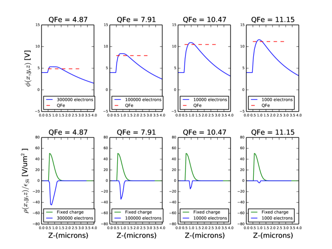
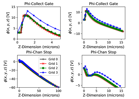
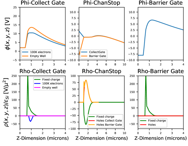
Because of the strong non-linearity, simply iterating is numerically unstable. The method that works, described in detail by Rafferty, et.al. [18] and buillding on the work of Gummel ([19]), is to take this last equation as a non-linear equation for in terms of and run a Newton’s method “inner loop” to find at each grid point. Then we iterate to convergence as before. This allows us to simultaneously solve for the potential and the carrier density. Of course, we just described the electron density here, but there is a similar equation for holes, but with opposite signs. Figure 3 shows an example of varying on the solution. Note that the quasi-Fermi level is constant in each region containing mobile carriers. In the CCD, each collecting well contains a different number of mobile carriers, so is constant in each well, but is different from well to well. However, when simulating the device, instead of knowing the value of , we typically know the number of electrons in each well. So how do we translate from the known number of electrons to the unknown value of ? The code provides two methods, selected by the value of the parameter “ElectronMethod”. With this parameter set to 1, a test simulation is run where the parameter (called QFe in the code) is varied through a range. For each value of QFe, we integrate over a pre-determined region to count the number of electrons in the well, building a look-up table of the number of electrons vs QFe. The results for a few values of QFe are shown in Figure 3. Then the code interpolates to determine the value of QFe which gives the appropriate number of electrons. In practice one can get close to the desired number of electrons, but the non-linearity causes variations from the desired number, so a second method was developed. When “ElectronMethod” has a value of 2, what is done is to place the correct number of electrons in the well, uniformly distributed in the center of the well. The code then moves the electrons around until the value of QFe is constant in the well. This allows one to get the correct number of electrons in the well without needing to know the value of the quasi-Fermi level.
There is one more complication. As discussed in Section 2.1, a non-linear Z-axis is used to concentrate grid cells in the bottom region where the potentials and charge densities are changing most strongly. In principle, any smooth funcation can be used for the Z-axis mapping. Here we chose an easily differentiable polynomial function of the following form, where z is the linear z coordinate, and zp is the non-linear coordinate, which is the actual value used in solving and plotting. Here is the silicon thickness, and NZExp is a user-defined constant that controls the non-linearity, as described in Figure 2.
| (14) |
The non-linear z-axis modifies Poisson’s equation from:
| (15) |
to:
| (16) |
In practice, the additional partial derivatives can be pre-computed, so this is simply accounted for in the discretized equations and has only a minor impact on the speed of iteration.
2.4 Multi-grid methods
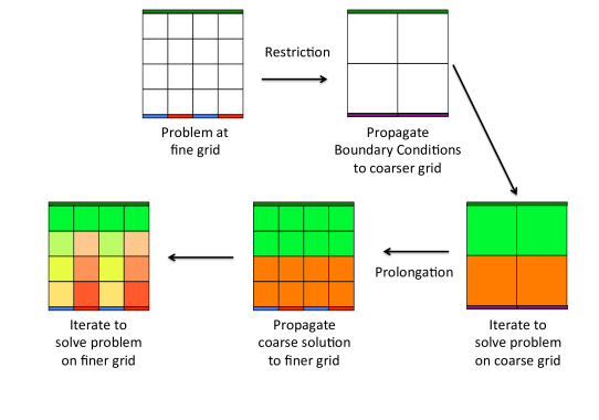
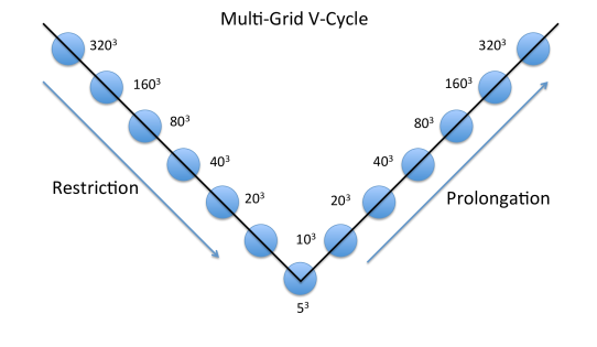
It is well known that multi-grid methods speed convergence of solutions to Poisson’s equation by getting correct solutions to the long-wavelength modes at a coarser grid where convergence is much more rapid. There is a wealth of literature on the subject, and Briggs [20] or Press [21] give excellent summaries. The basic idea is shown in Figure 4. In practice in this code, we have adopted a simpler method. Rather than use “Restriction” to propagate the boundary conditions down to the coarser grid, we simply set up the boundary conditions on all of the sub-grids at the outset of the problem. In addition, we have found that there is little value in running coarser grids than , because at this resolution the problem converges very rapidly. So for a typical problem which has perhaps grid cells, we define the finest grid and three subgrids, with the coarsest grid having grid cells. We then set up the boundary conditions on all of the subgrids, iterate the coarsest grid, “Prolongate” the solution up to the next grid, and continue until we have reached the finest grid.
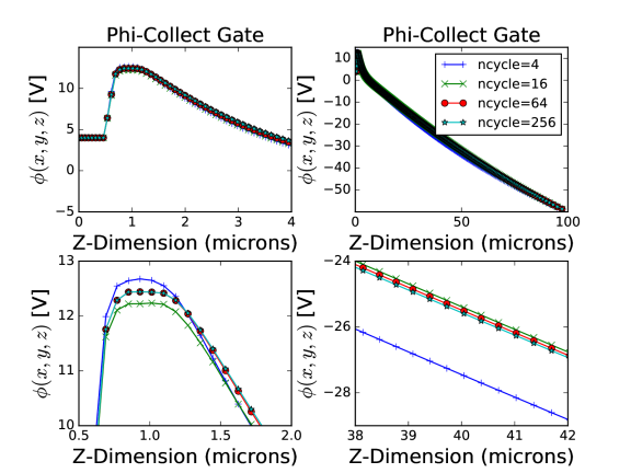
At this point it is appropriate to discuss the problem of convergence. Convergence of the SOR algorithm is notoriously slow. Multi-grid methods help a great deal, however, care must still be taken to ensure that the solution has converged adequately for your problem. The parameter “ncycle” controls the number of iterations taken at the finest grid. Each coarser grid increases the number of iterations by a factor of 4. So for example, a typical problem like one of the “pixel” examples, which has ncycle=128, the coarsest grid has 1/8 the resolution, and will run SOR cycles at the coarsest grid. Figures 5 and 6 show the convergence of a typical problem. For most problems, a value of ncycle=64 is adequate. The problems most dependent on accurate convergence have proven to be the pixel distortion simulations like those in Section 3.1. Since we are dealing with very small deviations in the pixel shapes due to the BF effect, it is important to make sure the results have converged.
2.5 Modeling carrier transport
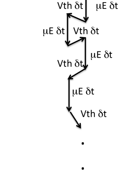
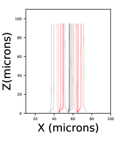
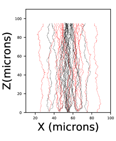
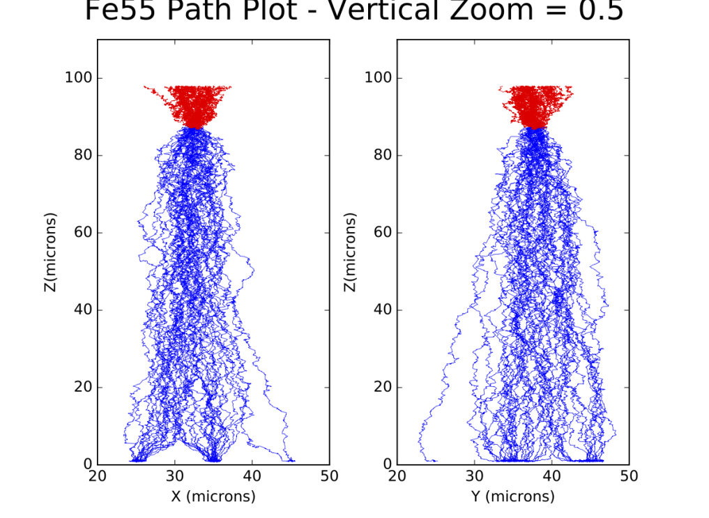
The basic scheme for modeling carrier transport is shown in Figure 7. Electrons are assumed to have lattice collisions on a time scale , which is on the order of picoseconds. At each collision, the electron is assumed to pick up a thermal velocity which is in a random direction. In addition to this thermal velocity, it also has a drift velocity given by , where the mobility is calculated as a function of electric field and temperature using the mobility model of Jacobini [22]. These two velocities are added vectorially and it travels in this direction at this velocity for a time until the next collision, and this continues until the electron reaches the bottom. The electron path is logged in the *_Pts.dat file. If the parameter “LogPixelPaths” is zero, only the initial and final positions are logged. If this parameter is one, the entire path is logged. The thermal velocity has a multiplier (“DiffMultiplier”) which can be used to tune the amount of diffusion. If this is set to zero, diffusion is turned off, with the impact as shown in Figure 8. A value has been found to accurately reproduce the amount of diffusion seen in data (see Section 3.2). Since the value of in the code is the bare electron mass, this value is equivalent to an electron effective mass of about 0.19. This is somewhat low, as Green [23] finds a value of 0.27. This value of DiffMultiplier is easily adjusted by the user, however.
The initial electron locations in X and Y can be determined in a number of ways, as determined by the “PixelBoundaryTestType” parameter. These include an equally spaced grid, a Gaussian spot, a random location within a boundary, an event, or reading in a list of locations. The starting location in Z can either be specified, or calculated given a filter band.
| Mobility: calculated from Jacobini model [22] |
| at |
| Collision time: |
| typically about 0.9 ps. |
| drawn from exponential distribution with mean of |
| Each thermal step in a random direction in 3 dimensions. |
| Typically about 1000 steps to propagate to the collecting well. |
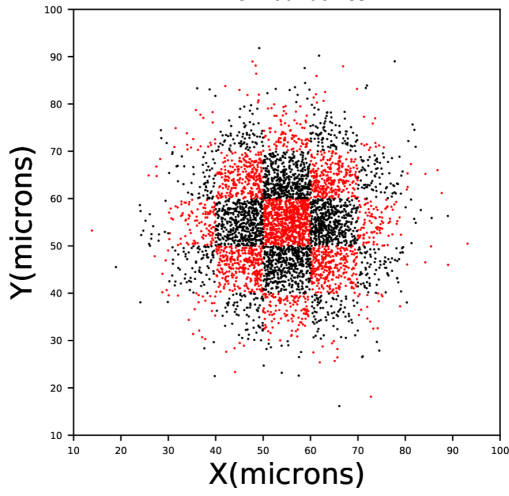
Diffusion turned off
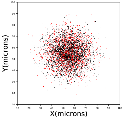
Realistic Diffusion
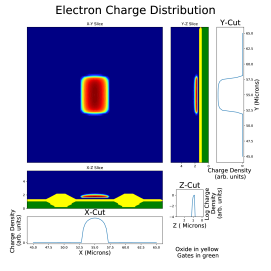
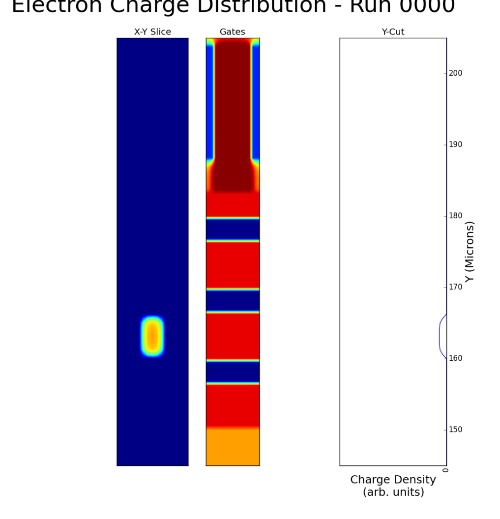
2.6 Example outputs
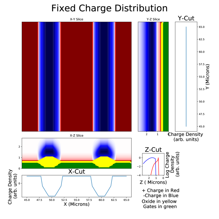
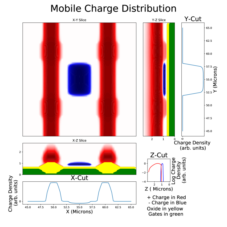
Once the simulation has run, the potential, electric fields, and charge carrier densities are available throughout the simulation volume. What one chooses to visualize depends on the problem being studied. Here we have chosen three examples (Figures 9, 10, and 11) of the type of data which is available.
3 Validation with measured data
To successfully model a CCD, an accurate physical characterization of the CCD is needed. Details such as dopant densities, layer thicknesses, and physical dimensions need to be known, at least approximately. For modeling the CCDs from the two vendors which will be used in the LSST camera, we obtained detailed physical measurements, which have been described in [16]. This has helped to make the simulations described in the next few sections as physically realistic as possible. Most of the plots in this section can be reproduced using the examples at the \carlitoPoisson_CCD code site at [2].
Regarding the parameters used in the simulations, there has been optimization of the numeric parameters, such as grid size, number of iterations, successive over-relation factor, etc. to ensure convergence and accuracy. However, the physical parameters, such as physical dimensions, voltages, doping levels, oxide thicknesses, etc. have all been directly measured. In particular, these parameters have not been tuned to improve the fit with measured data shown in the following examples.
3.1 Pixel distortions and pixel-pixel covariances
As has been extensively discussed in the literature ([11], [12], [13], [14]), as charge builds up in the central region of bright objects, the stored charge repels additional incoming charge and broadens the profile of these objects. The impact of the stored charge on the pixel shapes can be determined by measuring the pixel-pixel covariances on a large number of flat images ([11], [15]). These covariances are calculated from a large number of flat pairs of varying intensity (see [15] for example) as:
| (17) |
where is the difference in flux between the two flats at pixel i,j, and is the number of pixels summed over.
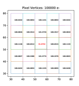
We have generated this data on a large number of flat pairs on LSST CCDs, measured on the UC Davis LSST beam simulator ([24], [14]), and would like to compare these results to simulations. For a dataset of 100 flat pairs, each with 16 million pixels with an average signal level of 50,000 electrons, this is approximately electrons. Directly simulating this data is out of the question. However, we have found a simple way to run a single simulation which reproduces the measured pixel covariances. In order to do this, we first simulate a situation where one pixel has a fixed amount of charge (typically 100,000 electrons), and all surrounding pixels are empty. After solving for the potential and resulting electric field, we can track electrons down through the silicon. As the electrons travel down through the silicon under the influence of the electric field, they eventually end up in one of the collecting wells. A binary search is used to find the bifurcation points where electrons on one side of the bifurcation point end up in one pixel, and electrons on the other side of the bifurcation point end up in an adjacent pixel. This binary search is performed with diffusion turned off in order not to introduce a stochastic element into the electron paths. These bifurcation points are identifed as the pixel boundaries. This allows us to characterize the distortion in the pixel boundaries which results from the central pixel charge. A typical result of this process is shown in Figure 12. The number of vertices used to define the distorted pixel shapes is an adjustable parameter. A minimum of 12 vertices is needed to adequately define the distortion (4 corners plus 2 points per edge). The distorted pixels shown in Figure 12 and used in Figure 13 were simulated with a total of 132 vertices (4 corners plus 32 points per edge). The distorted pixel shapes which result are what gives rise to the BF effect, with the central pixel losing area, which is gained by the surrounding pixels.
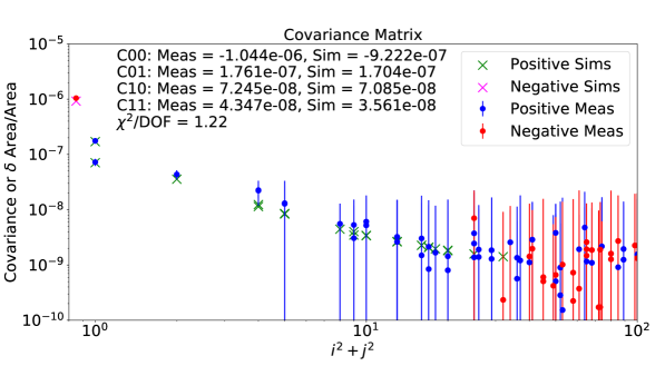
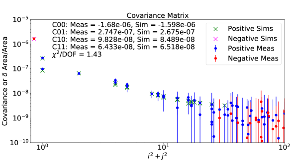
We find that the area distortions which result accurately capture the measured pixel-pixel covariances. Figure 13 shows the agreement between the measured pixel-pixel covariances on flat field images and the simulated area distortions, as measured and as simulated on LSST CCDs from both CCD vendors. The agreement is quite good. The asymmetry of the nearest neighbor pixels is correctly modeled, and the simulated values agree with the measurements within the statistical errors. These simulations are run with the “pixel-itl.cfg” and “pixel-e2v.cfg” examples at [2]. More details on these measurements and simulations are given in [14] and [25].
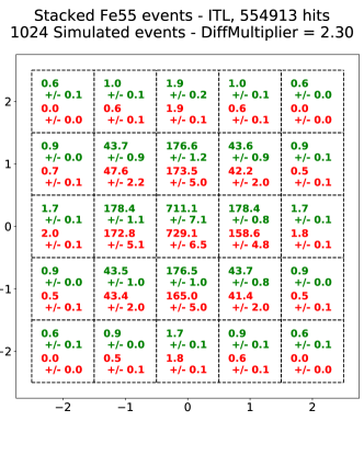
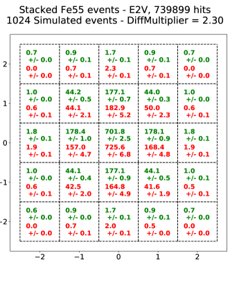
3.2 Diffusion modeling and Fe55 tests
CCDs are routinely characterized by exposing the CCD to an source. (see [26], for example). The radioactive decay produces X-rays with a known energy, with the peak being the strongest peak, typically producing 1620 hole-electron pairs when photoelectrically absorbed in the silicon. These carriers then propagate down to the collecting wells, where they are collected and counted. Because of diffusion, the carriers, which are initially produced in a small volume, spread out and occupy several pixels. To simulate these events, a special module was written. Normally photoelectrons propagate one at a time, without influence from neighboring carriers. But the carriers produced in the event are produced in a short time, so interactions between the carriers might be important. The code takes the like carrier repulsion and opposite carrier attraction into account, and the parameters “Fe55ElectronMult” and “Fe55HoleMult” can be used to turn off or modify this interaction if desired. Figure 14 shows a typical event, and Figure 15 shows stacked pixel maps compared between measurements and simulations. The spread of the charge cloud due to diffusion is well modeled. This simulation is run with the “fe55.cfg” example at [2].
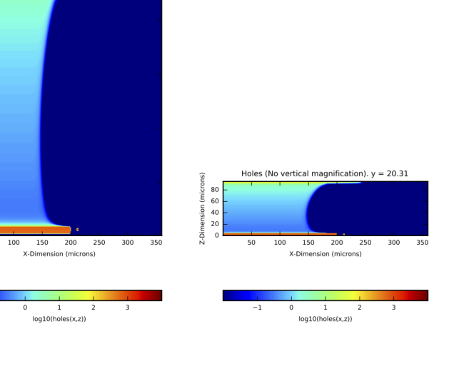
3.3 Saturation and blooming
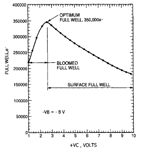
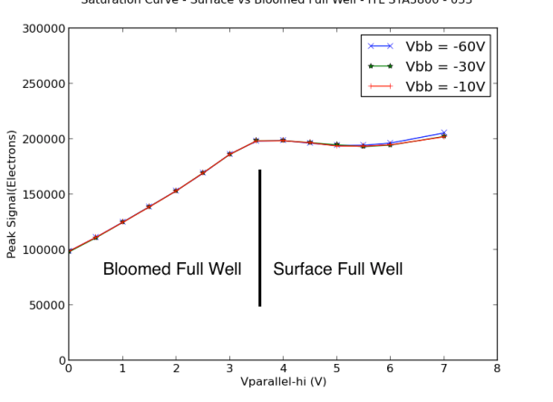
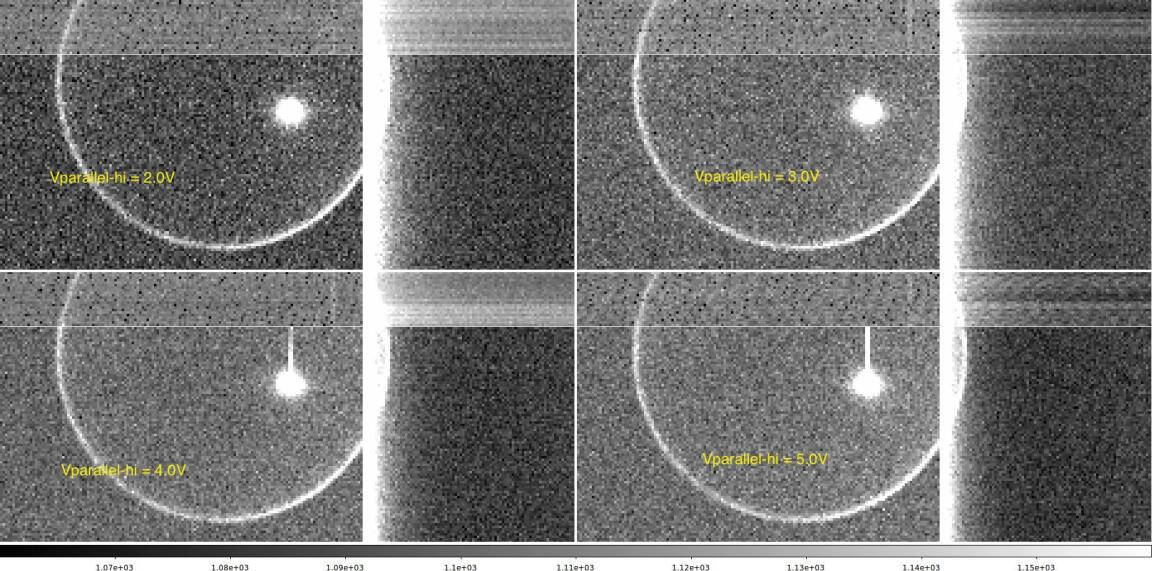
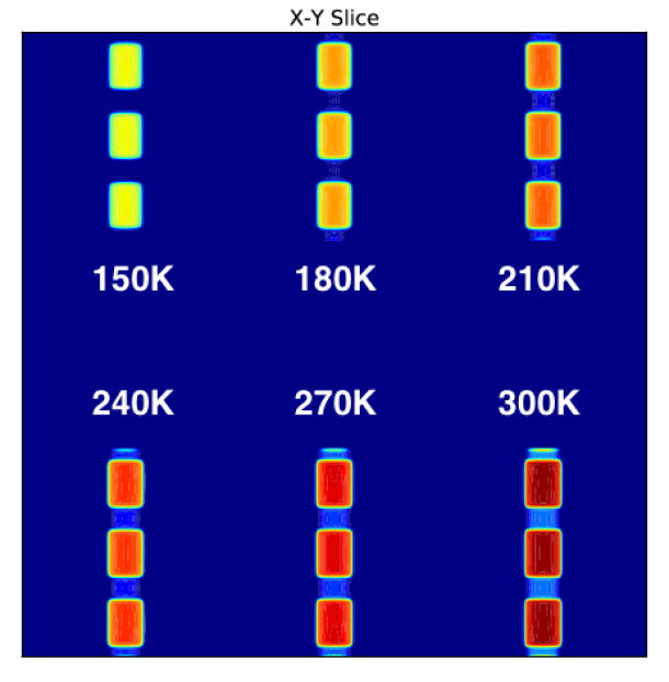
A large number of simulations have been run to better understand saturation and blooming in the ITL STA3800C device. These simulations have been very helpful to understand the physics of the device, because in the simulator one can get information which is simply not accessible to measurement. Figure 16 shows the distinction between the “bloomed full well” condition, where charge begins to bloom above the charge storage regions, and the “surface full well” condition, where charge blooms along the silicon surface. This effect is discussed in detail in Janesick [26]. The simulations in Figures 17 and 18 reproduce these conditions, and these simulations illustrate the difference between these conditions. Measurements of saturated spots in the surface full well condition, shown in Figure 19 also show that in the surface full well condition, charge is lost to traps at the silicon-silicon dioxide interface. Thus it is apparent that the surface full well condition is to be avoided.
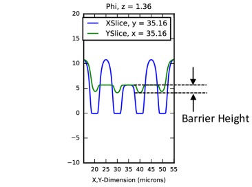
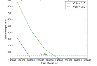
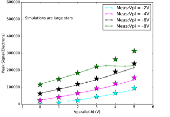
We can go further and quantitatively reproduce measurements of the onset of saturation as a function of parallel low and high voltages, as shown in Figure 20. By quantifying the barrier height between the storage wells, we show that saturation occurs when the barrier height drops below a certain value. The fit is good except in the strong surface full well condition, because the charge loss that occurs is not included in the simulations. It would be possible to modify the simulations to include this effect, but since the surface full well condition is to be avoided, this was deemed to be not worth the effort.
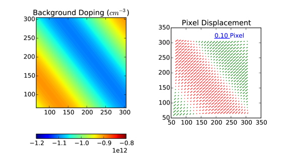
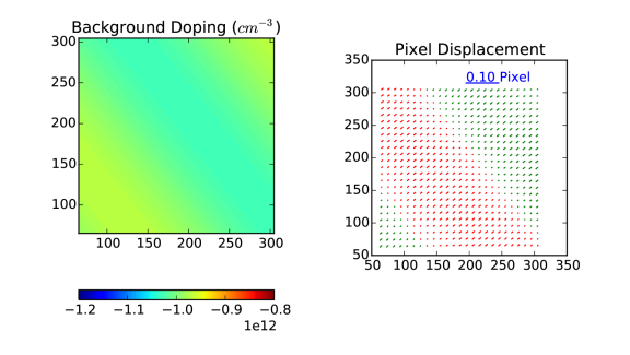
3.4 Astrometric shifts at array edges
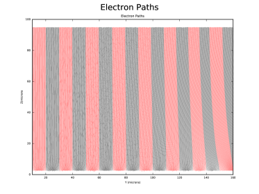
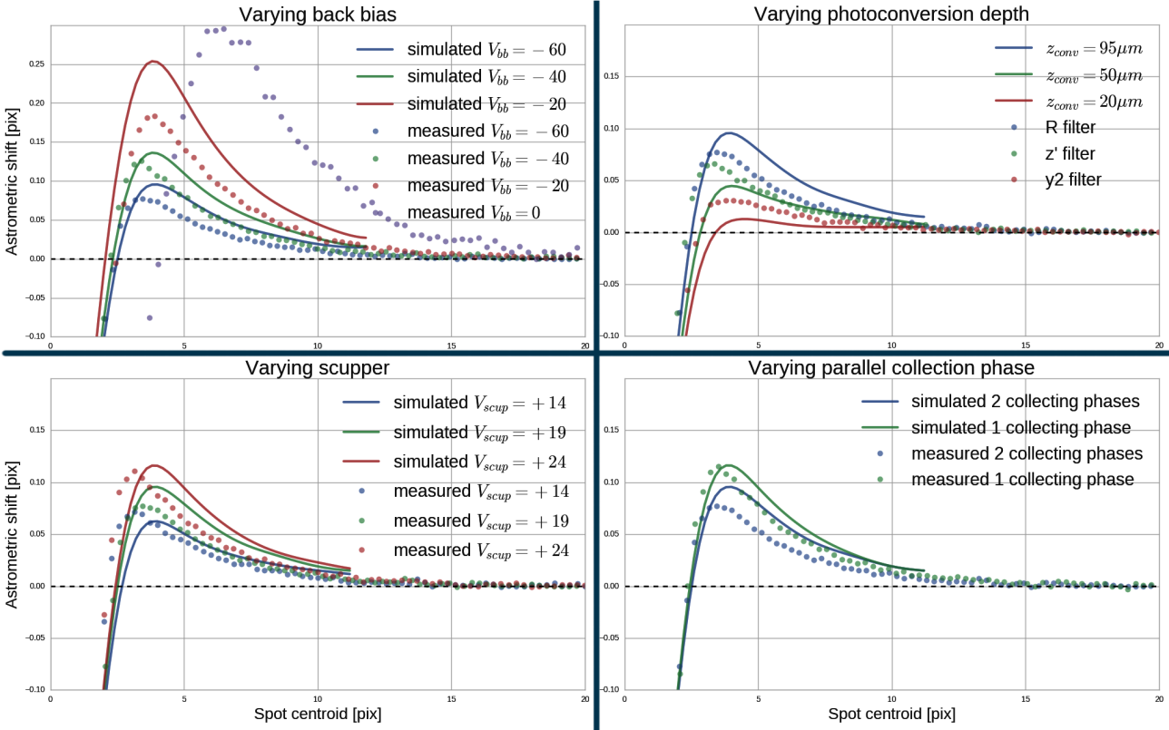
In addition to simulations of the pixel arrays, simulations can be done of the peripheral circuitry, as shown in the next two sections. At the edges of the pixel array, lateral electric fields from the surrounding circuitry can introduce pixel boundary shifts, which lead to measurable astrometric shifts. This effect has been characterized on the UC Davis LSST Optical Simulator ([24], [27]). We have then built a simulation of a portion of the pixel array which extends to the chip edge to compare the measurements to the simulations. In addition to the pixel array, it is necessary to build into the simulation the appropriate “fixed voltage regions” at the edge of the chip. Figure 21 shows the setup of this simulation. The bending of the equipotential lines near the edge of the pixel array betray the presence of a lateral electric field which deflects incoming electrons. Figure 22 shows these simulated paths (with diffusion turned off), and the edge deflection is apparent. In addition to this deflection, there is a second effect which influences the astrometric shift, which is that as the measured spot begins to “fall off’ the edge of the array, there is a resulting shift in the opposite direction. These two competing effects lead to the astrometric shifts seen in Figure 23. The shift has been characterized for a number of different measurement conditions. The simulation, while not perfect, captures all of the trends correctly. These simulations are run with the “edge.cfg” example at [2].
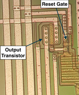
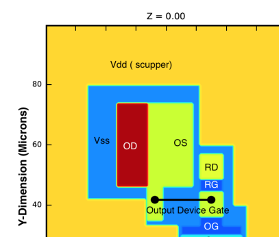
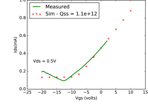
3.5 Output transistor characteristics
This section shows simulations that were done to model the output transistor of the ITL STA3800C. Figure 24 shows the simulated and measured characteristics. We obtained a relatively good fit of the transistor turn-on. This simulation is run with the “trans.cfg” example at [2].
3.6 Other qualitative tests
Some other tests have been run which have given results which are qualitatively reasonable, but which have not been compared with quantitative measurements, and three of these are reviewed here. The first of these are known as “tree rings”. As is well known, periodic dopant variations introduced during the growth of the silicon boule can lead to measurable variations in flat fields, as well as introducing astrometric pixel shifts (see, for example, [10]). This effect has been successfully simulated, as shown in Figure 25. This simulation is run with the “treering.cfg” example at [2].
A second interesting simulation is of the backside substrate connection . It is often questioned how this bias voltage, which is only connected to the CCD frontside, is conducted to the backside when the CCD is fully depleted. The answer is that there is an undepleted region near the chip edge which serves this purpose. It is interesting to simulate this connection, and the result is shown in Figure 26.
While the simulator solves for the condition of the CCD in equilibrium, and does not do transient simulations, it is possible to simulate transient effects by repeatedly solving for the state of the CCD with small incremental changes to the boundary conditions. These can then be stitched together to form a movie of the results. An example of the parallel charge transport is shown in Figure 27. Several movies constructed in this way are available at [2].
4 Conclusion
We have presented a software package optimized for simulating astronomical CCDs. The code has been optimized to be as physically realistic as possible, and accurately simulates many aspects of CCD behavior. The package is open source and freely available [2], and has been validated against a number of different types of CCD measurements. It has proven useful for analyzing sensor effects in the CCDs being used to construct the LSST focal plane, and insights gained from running these simulations are being incorporated into the software stack to be used for instrument signature removal in the LSST images. It is hoped that it will find additional uses in the future.
5 Acknowledgements
Kirk Gilmore’s help in setting up the hardware and software for the CCDs from both vendors has also been invaluable. Perry Gee has provided key support in software and networking. Merlin Fisher-Levine has patiently helped with my understanding and implementation of the LSST data management software stack. David Kirkby contributed code for including different filters. For author contributions, C.L. developed the \carlitoPoisson_CCD code, ran most of the studies described here, and drafted the paper. AB carried out the study of astrometric shifts at array edges, and provided test and debug support. JAT supervised the project. Financial support from DOE grant DE-SC0009999 and Heising-Simons Foundation grant 2015-106 are gratefully acknowledged. This paper has undergone internal review in the LSST Dark Energy Science Collaboration. The internal reviewers were Andrew Rasmussen, Douglas Tucker, and Dan Weatherill, and their inputs are much appreciated.
References
- [1] G.E. Smith. Nobel lecture: The invention and early history of the ccd. Rev. Mod. Phys., 82:2307–2312, Aug 2010.
- [2] C. Lage. Poisson solver for LSST CCDs, November 2019. https://github.com/craiglagegit/Poisson_CCD.
- [3] Ž. Ivezić, S. M. Kahn, J. A. Tyson, B. Abel, E. Acosta, R. Allsman, D. Alonso, Y. AlSayyad, S. F. Anderson, J. Andrew, and et al. LSST: From Science Drivers to Reference Design and Anticipated Data Products. Astrophys. J., 873:111, March 2019.
- [4] P. O’Connor. Uniformity and Stability of the LSST Focal Plane, 2019. arXiv:1907.00995.
- [5] P. O’Connor, P. Antilogus, P. Doherty, J. Haupt, S. Herrmann, M. Huffer, C. Juramy-Giles, J. Kuczewski, S. Russo, C. Stubbs, and R. Van Berg. Integrated system tests of the LSST raft tower modules. In Andrew D. Holland and James Beletic, editors, High Energy, Optical, and Infrared Detectors for Astronomy VII, volume 9915, pages 327 – 338. International Society for Optics and Photonics, SPIE, 2016.
- [6] University of Arizona. Imaging Technology Laboratory, 2016. http://www.itl.arizona.edu.
- [7] Teledyne E2V, 2019. https://www.teledyne-e2v.com/products/space/.
- [8] J. Villasenor, G. Prigozhin, J.P. Doty, C. Lage, S. Yazdi, G. Ricker, and R. Vanderspek. Reach-through effect in deep depletion TESS CCDs. Journal of Instrumentation, 12(04):C04025–C04025, apr 2017.
- [9] A. Hadjidimos. Successive overrelaxation (sor) and related methods. Journal of Computational and Applied Mathematics, 123(1):177–199, 2000. Numerical Analysis 2000. Vol. III: Linear Algebra.
- [10] A. A. Plazas, G. M. Bernstein, and E. S. Sheldon. On-Sky Measurements of the Transverse Electric Fields’ Effects in the Dark Energy Camera CCDs. Pub. Astron. Soc. Pacific, 126(942):750, Aug 2014.
- [11] P. Antilogus, P. Astier, P. Doherty, A. Guyonnet, and N. Regnault. The brighter-fatter effect and pixel correlations in CCD sensors. Journal of Instrumentation, 9:C03048, March 2014.
- [12] D. Gruen, G. M. Bernstein, M. Jarvis, B. Rowe, V. Vikram, A. A. Plazas, and S. Seitz. Characterization and correction of charge-induced pixel shifts in DECam. Journal of Instrumentation, 10:C05032, May 2015.
- [13] A. Guyonnet, P. Astier, P. Antilogus, N. Regnault, and P. Doherty. Evidence for self-interaction of charge distribution in charge-coupled devices. Astro. & Astrophys., 575:A41, March 2015.
- [14] C. Lage, A. Bradshaw, and J. A. Tyson. Measurements and simulations of the brighter-fatter effect in CCD sensors. Journal of Instrumentation, 12:C03091, Mar 2017.
- [15] W.R. Coulton, R. Armstrong, K.M. Smith, R.H. Lupton, and D.N. Spergel. Exploring the Brighter-fatter Effect with the Hyper Suprime-Cam. The Astronomical Journal, 155(6):258, May 2018.
- [16] C. Lage. Physical and electrical analysis of LSST sensors, 2019. https://arxiv.org/abs/1911.09577.
- [17] S.M. Sze. Physics of Semiconductor Devices. Wiley-Interscience publication. John Wiley & Sons, 1981.
- [18] C.S. Rafferty, M.R. Pinto, and R.W. Dutton. Iterative methods in semiconductor device simulation. IEEE Transactions on Electron Devices, 32(10):2018–2027, 1985.
- [19] H. K. Gummel. A self-consistent iterative scheme for one-dimensional steady state transistor calculations. IEEE Transactions on Electron Devices, 11(10):455–465, 1964.
- [20] W.L. Briggs, S.F. McCormick, et al. A multigrid tutorial, volume 72. Siam, 2000.
- [21] W. H. Press, S. A. Teukolsky, W. T. Vetterling, and B. P. Flannery. Numerical Recipes. Cambridge University Press, third edition, 2007.
- [22] C. Jacobini, C. Canali, G.. Ottaviani, and A. Quaranta. A review of some transport properties of silicon. Solid-State Electronics, 20:77–89, 1977.
- [23] M.A. Green. Intrinsic concentration, effective densities of states, and effective mass in silicon. Journal of Applied Physics, 67(6):2944–2954, 1990.
- [24] J. A. Tyson, J. Sasian, K. Gilmore, A. Bradshaw, C. Claver, M. Klint, G. Muller, G. Poczulp, and E. Resseguie. LSST optical beam simulator. In High Energy, Optical, and Infrared Detectors for Astronomy VI, volume 9154 of Society of Photo-Optical Instrumentation Engineers (SPIE) Conference Series, page 915415, July 2014.
- [25] C. Lage. Linearity and correction of the BF effect in LSST sensors, 2019. https://arxiv.org/abs/1911.09567.
- [26] J.R. Janesick. Scientific Charge-coupled Devices. Press Monograph Series. SPIE Press, 2001.
- [27] A. Bradshaw, C. Lage, E. Resseguie, and J. A. Tyson. Mapping charge transport effects in thick CCDs with a dithered array of 40,000 stars. Journal of Instrumentation, 10:C04034, April 2015.
Appendix A List of configuration parameters
| Name | type | Default | Description |
| AddTreeRings | int | 0 | 0-No tree rings, 1-Add tree rings |
| BackgroundDoping | float | -1e+12 | Background doping in |
| BottomSteps | int | 1000 | Number of diffusion steps each electron takes |
| while logging final charge location | |||
| BuildQFeLookup | int | 0 | 0-Don’t build look-up table, 1-build look-up table |
| CCDTemperature | float | 173.00 | Temperature in K |
| CalculateZ0 | int | 0 | 0 - don’t calculate - Use ElectronZ0, |
| 1 - calculate from filter and SED. | |||
| ChannelDepth | float | 1.00 | Square profile depth in microns |
| ChannelDoping | float | 5e+11 | Square profile doping in |
| ChannelDose | float | 5e+11 | Gaussian profile dose in |
| ChannelPeak | float | 0.00 | Gaussian peak depth in microns |
| ChannelProfile | int | 0 | 0 = Square profile, N = N Gaussian profiles |
| ChannelSigma | float | 0.50 | Gaussian sigma in microns |
| ChannelStopDepth | float | 1.00 | Square profile depth in microns |
| ChannelStopDoping | float | 5e+11 | Square profile doping in |
| ChannelStopDose | float | 5e+11 | Gaussian profile dose in |
| ChannelStopDotCenter | float | 5.00 | Center position in microns from pixel bottom |
| ChannelStopDotDepth | float | 1.00 | Square profile depth in microns |
| ChannelStopDotDoping | float | 5e+11 | Square profile doping in |
| ChannelStopDotDose | float | 5e+11 | Gaussian profile dose in |
| ChannelStopDotHeight | float | 0.00 | Height in microns |
| ChannelStopDotPeak | float | 0.00 | Gaussian peak depth in microns |
| ChannelStopDotProfile | int | 0 | 0 = Square profile, N = N Gaussian profiles |
| ChannelStopDotSigma | float | 0.50 | Gaussian sigma in microns |
| ChannelStopDotSurfaceCharge | float | 0.00 | Surface charge in |
| ChannelStopPeak | float | 0.00 | Gaussian peak depth in microns |
| ChannelStopProfile | int | 0 | 0 = Square profile, N = N Gaussian profiles |
| ChannelStopSideDiff | float | FieldOxideTaper | Side diffusion in microns |
| ChannelStopSigma | float | 0.50 | Gaussian sigma in microns |
| ChannelStopSurfaceCharge | float | 0.00 | Surface charge in |
| ChannelStopWidth | float | 1.00 | Width in microns |
| ChannelSurfaceCharge | float | 0.00 | Surface charge in |
| CollectedCharge[i][j] | int | 0 | Number of electron in well i,j |
| CollectingPhases | int | 1 | Number of collecting phases |
| Continuation | int | 0 | 0-No continuation, 1-continue at LastCont..Step |
| DiffMultiplier | float | 2.30 | Used to adjust amount of diffusion |
| ElectronMethod | int | 0 | Controls electron calculation |
| 0 - Leave electrons where they land from tracking (old) | |||
| 1 - Set QFe (QFe is always used in Fixed Regions) | |||
| If 1 is specified, you must provide QFe lookup params | |||
| 2 - Electron conservation and constant QFe (best) | |||
| ElectronZ0Area | float | 100.00 | Initial Z value for electrons calculating pixel areas |
| ElectronZ0Fill | float | 100.00 | Initial Z value for electrons filling pixel wells |
| EquilibrateSteps | int | 100 | Number of diffusion steps each electron takes after |
| reaching bottom and before beginning to log charge. |
| Name | type | Default | Description |
| Fe55CloudRadius | float | 0.20 | Cloud radius in microns |
| Fe55ElectronMult | float | 1.00 | Used to adjust cloud electron attraction/repulsion |
| Fe55HoleMult | float | 1.00 | Used to adjust cloud hole attraction/repulsion |
| FieldOxide | float | 0.40 | Thickness in microns |
| FieldOxideTaper | float | 0.50 | Taper width in microns |
| FilledPixelCoords[i][j] | float | 2.00 | Center x,y (in microns) of well i,j |
| FilterBand | str | none | One of u,g,r,i,z,y |
| FilterFile | str | notebooks/depth_pdf.dat | SED file |
| FixedRegionBCType | int | 0 | Fixed region description |
| FixedRegionDoping | int | 0 | Fixed region description |
| FixedRegionOxide | int | 0 | Fixed region description |
| FixedRegionQFe | float | 100.00 | Fixed region description |
| FixedRegionQFh | float | -100.00 | Fixed region description |
| FixedRegionVoltage | float | 0.00 | Fixed region description |
| FringeAngle | float | 0.00 | Fringe parameter for PixelBoundaryTestType=3 |
| FringePeriod | float | 0.00 | Fringe parameter for PixelBoundaryTestType=3 |
| GateGap | float | 0.00 | Gap between paralel gates in microns (experimental) |
| GateOxide | float | 0.15 | Thickness in microns |
| GridsPerPixelX | int | 16 | Grids per pixel at ScaleFactor = 1 |
| GridsPerPixelY | int | 16 | Grids per pixel at ScaleFactor = 1 |
| LastContinuationStep | int | 0 | Used when continuing a stopped simulation |
| LogEField | int | 0 | 0 - don’t calculate E-Field, 1 - Calc. and store E-Field |
| LogPixelPaths | int | 0 | 0 - only the final (z 0) point is logged, |
| 1 - Entire path is logged | |||
| NQFe | int | 81 | Number of steps in QFe look-up table |
| NZExp | float | 10.00 | Non-linear z axis exponent |
| NumDiffSteps | int | 1 | A speed/accuracy trade-off. A value of 1 uses the |
| theoretical diffusion step. A higher value takes | |||
| larger steps. Experimental | |||
| NumElec | int | 1000 | Number of electrons to be traced between field recalc. |
| NumPhases | int | 3 | Number of parallel phases |
| NumSteps | int | 100 | Number of steps, each one adding NumElec electrons |
| NumVertices | int | 2 | Number of vertices per side for the pixel area calc. |
| Since there are also 4 corners, there will be: | |||
| (4 * NumVertices + 4) vertices in each pixel | |||
| NumberofFilledWells | int | 0 | Self-explanatory |
| NumberofFixedRegions | int | 0 | Self-explanatory |
| NumberofPixelRegions | int | 0 | Self-explanatory |
| Nx | int | 160 | Number of grids in x at ScaleFactor = 1 |
| Ny | int | 160 | Number of grids in y at ScaleFactor = 1 |
| Nz | int | 160 | Number of grids in z at ScaleFactor = 1 |
| Nzelec | int | 32 | No. grids in z in elec & hole grids at ScaleFactor = 1 |
| PhotonList | str | PhotonList | Photon list filename |
| PixelAreas | int | 0 | -1 - Don’t calc areas, N - calc areas every Nth step |
| PixelBoundaryLowerLeft | float | 2.00 | x,y coordinates of PixelBoundary lower left corner |
| PixelBoundaryNx | int | 9 | Number of pixels in PixelBoundary |
| PixelBoundaryNy | int | 9 | Number of pixels in PixelBoundary |
| PixelBoundaryStepSize | float | 2.00 | Used with PixelBoundaryTestType=0 |
| PixelBoundaryTestType | int | 0 | 0-Trace uniform grid, 1-TraceGaussian spot, |
| 2,4-TraceRegion, 5-TraceList, 6-Fe55 cloud. |
| Name | type | Default | Description |
|---|---|---|---|
| PixelBoundaryUpperRight | float | 2.00 | x,y coordinates of PixelBoundary lower left corner |
| PixelRegionLowerLeft | float | 2.00 | PixelRegion is used for PBTestType 0,2,4 |
| PixelRegionUpperRight | float | 2.00 | PixelRegion is used for PBTestType 0,2,4 |
| PixelSizeX | float | -1.00 | Pixel size in microns |
| PixelSizeY | float | -1.00 | Pixel size in microns |
| QFemax | float | 10.00 | Max QFe in look-up table |
| QFemin | float | 5.00 | Min QFe in look-up table |
| SaturationModel | int | 0 | Experimental |
| SaveData | int | 1 | 0 - Save only Pts, N save phi,rho,E every Nth step |
| SaveElec | int | 1 | 0 - Save only Pts, N save Elec every Nth step |
| SaveMultiGrids | int | 0 | 0 - Don’t save subgrids, 1 - Save all of the grids at all scales |
| ScaleFactor | int | 1 | Power of 2 that sets the grid size |
| Seed | int | 77 | Pseudo random number seed |
| SensorThickness | float | 100.00 | Sensor Thickness in microns |
| Sigmax | float | 1.00 | Gaussian spot sigma in microns |
| Sigmay | float | 1.00 | Gaussian spot sigma in microns |
| SimulationRegionLowerLeft | float | 2.00 | x,y coordinates of lower left corner of entire simulation |
| TopAbsorptionProb | float | 0.00 | Probability an electron is absorbed if it reaches the top surface |
| TreeRingAmplitude | float | 0.00 | Fractional amplitude (i.e. 0.10 is a 10% variation) |
| TreeRingAngle | float | 0.00 | Direction of variation in degrees (0:constant in x) |
| TreeRingPeriod | float | 0.00 | Period of sinusoidal variation in microns |
| Vbb | float | -50.00 | Back bias voltage |
| VerboseLevel | int | 1 | 0 - minimal output, 1 - normal, 2 - more verbose 3-dump everything |
| Vparallel_lo | float | -8.00 | Parallel Low Voltage |
| Vparallel_hi | float | 4.00 | Parallel High Voltage |
| XBCType | int | 1 | 0 - Free BC, 1 - Periodic BC |
| Xoffset | float | 0.00 | Shift of Gaussian spot center |
| YBCType | int | 1 | 0 - Free BC, 1 - Periodic BC |
| Yoffset | float | 0.00 | Shift of Gaussian spot center |
| iterations | int | 1 | Number of VCycles |
| ncycle | int | 100 | Number of SOR cycles at each resolution |
| outputfilebase | str | Test | Output filename base |
| outputfiledir | str | data | Output filename directory |
| qfh | float | -100.00 | Hole quasi-Fermi level - applies everywhere except Fixed regions |
| w | float | 1.90 | Successive Over-Relaxation factor |
Appendix B Description of example configuration files included with the code.
The figures in this paper were generated with v1.0 of the \carlitoPoisson_CCD code, at [2]. There are a total of 14 examples included with the code. Each example is in a separate directory in the data directory, and has a configuration file of the form *.cfg. The parameters in the *.cfg files are commented to explain (hopefully) the purpose of each parameter, and a detailed listing of all configuration parameters is in Appendix A. Python plotting routines are included with instructions below on how to run the plotting routines and the expected output. The plot outputs are placed in the data/*/plots files, so you can see the expected plots without having to run the code. If you edit the .cfg files, it is likely that you will need to customize the Python plotting routines as well. The estimated run times given here are what was seen on a dual-core 1.4 GHz Intel Core i5 laptop computer.
-
•
Example 1: data/smallpixel/smallpixel.cfg
-
1.
Purpose: A single pixel and surroundings. The central pixel contains 100,000 electrons. No electron tracking or pixel boundary plotting is done. The subgrids are saved so one can look at convergence. This is useful for getting things set up rapidly
-
2.
Syntax: src/Poisson data/smallpixel/smallpixel.cfg
-
3.
Expected run time: .
-
4.
Plot Syntax: python pysrc/Poisson_Small.py data/smallpixel/smallpixel.cfg 0
-
5.
Plot Syntax: python pysrc/Poisson_Convergence.py data/smallpixel/smallpixel.cfg 0
-
1.
-
•
Example 2: data/pixel0/pixel.cfg
-
1.
Purpose: A 9x9 grid of pixels at low resolution (ScaleFactor=1). The central pixel contains 100,000 electrons. No electron tracking or pixel boundary plotting is done.
-
2.
Syntax: src/Poisson data/pixel0/pixel.cfg
-
3.
Expected run time: .
-
4.
Plot Syntax: python pysrc/Poisson_Plots.py data/pixel0/pixel.cfg 0
-
5.
Plot Syntax: python pysrc/ChargePlots.py data/pixel0/pixel.cfg 0 2
-
1.
-
•
Example 3: data/pixel-itl/pixel.cfg
-
1.
Purpose: A 9x9 grid of pixels at higher resolution (ScaleFactor=2). The central pixel contains 100,000 electrons. The parameters are set up for the ITL STA3800C CCD. This should give physically meaningful results, and is what was used in the published papers. After solving Poisson’s equation, electron tracking is done to determine the pixel distortions.
-
2.
Syntax: src/Poisson data/pixel-itl/pixel.cfg
-
3.
Expected run time: .
-
4.
Plot Syntax: python pysrc/Poisson_Plots.py data/pixel-itl/pixel.cfg 0
-
5.
Plot Syntax: python pysrc/ChargePlots.py data/pixel-itl/pixel.cfg 0 2
-
6.
Plot Syntax: python pysrc/VertexPlot.py data/pixel-itl/pixel.cfg 0 2
-
7.
Plot Syntax: python pysrc/Area_Covariance_Plot.py data/pixel-itl/pixel.cfg 0
-
1.
-
•
Example 4: data/pixel-e2v/pixel.cfg
-
1.
Purpose: A 9x9 grid of pixels at higher resolution (ScaleFactor=2). The central pixel contains 100,000 electrons. The parameters are set up for the E2V CCD250 CCD. This should give physically meaningful results, and is what was used in the published papers. After solving Poisson’s equation, electron tracking is done to determine the pixel distortions.
-
2.
Syntax: src/Poisson data/pixel-e2v/pixel.cfg
-
3.
Expected run time: .
-
4.
Plot Syntax: python pysrc/Poisson_Plots.py data/pixel-e2v/pixel.cfg 0
-
5.
Plot Syntax: python pysrc/ChargePlots.py data/pixel-e2v/pixel.cfg 0 2
-
6.
Plot Syntax: python pysrc/VertexPlot.py data/pixel-e2v/pixel.cfg 0 2
-
7.
Plot Syntax: python pysrc/Area_Covariance_Plot.py data/pixel-e2v/pixel.cfg 0
-
1.
-
•
Example 5: data/pixel1/pixel.cfg
-
1.
Purpose: A 9x9 grid of pixels at higher resolution (ScaleFactor=2). The central pixel contains 100,000 electrons. The parameters are set up for the ITL STA3800C CCD. This is included as an example of ElectronMethod=1, which iterates to find the value of the electron Quasi-Fermi level. After solving Poisson’s equation, electron tracking is done to determine the pixel distortions.
-
2.
Syntax: src/Poisson data/pixel1/pixel.cfg
-
3.
Expected run time: .
-
4.
Plot Syntax: python pysrc/Poisson_Plots.py data/pixel1/pixel.cfg 0
-
5.
Plot Syntax: python pysrc/ChargePlots.py data/pixel1/pixel.cfg 0 2
-
6.
Plot Syntax: python pysrc/VertexPlot.py data/pixel1/pixel.cfg 0 2
-
7.
Plot Syntax: python pysrc/Area_Covariance_Plot.py data/pixel1/pixel.cfg 0
-
1.
-
•
Example 6: data/smallcapf/smallcap.cfg
-
1.
Purpose: A simple field oxide capacitor for testing convergence.
-
2.
Syntax: src/Poisson data/smallcapf/smallcap.cfg
-
3.
Expected run time: .
-
4.
Plot Syntax: python pysrc/Poisson_CapConvergence.py data/smallcapf/smallcap.cfg 0
-
1.
-
•
Example 7: data/smallcapg/smallcap.cfg
-
1.
Purpose: A simple gate oxide capacitor for testing convergence.
-
2.
Syntax: src/Poisson data/smallcapg/smallcap.cfg
-
3.
Expected run time: .
-
4.
Plot Syntax: python pysrc/Poisson_CapConvergence.py data/smallcapg/smallcap.cfg 0
-
1.
-
•
Example 8: data/edgerun/edge.cfg
-
1.
Purpose: A simulation of the pixel distortion at the top and bottom edges of the ITL STA3800C CCD.
-
2.
Syntax: src/Poisson data/edgerun/edge.cfg
-
3.
Expected run time: .
-
4.
Plot Syntax: python pysrc/Poisson_Edge.py data/edgerun/edge.cfg 0
-
5.
Plot Syntax: python pysrc/Pixel_Shift.py data/edgerun/edge.cfg 0
-
1.
-
•
Example 9: data/iorun/io.cfg
-
1.
Purpose: A simulation of the output transistor region of the ITL STA3800C CCD, including the last few serial stages.
-
2.
Syntax: src/Poisson data/iorun/io.cfg
-
3.
Expected run time: .
-
4.
Plot Syntax: python pysrc/Poisson_IO.py data/iorun/io.cfg 0
-
5.
Plot Syntax: python pysrc/ChargePlots_IO.py data/iorun/io.cfg 0
-
1.
-
•
Example 10: data/treering/treering.cfg
-
1.
Purpose: A simulation of a 9x9 pixel region with a sinusoidal treering dopant variation introduced, so one can see the resulting pixel distortions.
-
2.
Syntax: src/Poisson data/treering/treering.cfg
-
3.
Expected run time: .
-
4.
Plot Syntax: python pysrc/VertexPlot.py data/treering/treering.cfg 0 4
-
1.
-
•
Example 11: data/fe55/pixel.cfg
-
1.
Purpose: A simulation of a 5x5 pixel region with a single Fe55 event above the center pixel. To determine the distribution of pixel counts, one needs to run many of these simulations with a random center point.
-
2.
Syntax: src/Poisson data/fe55/pixel.cfg
-
3.
Expected run time: .
-
4.
Plot Syntax: python pysrc/Poisson_Fe55.py data/fe55/pixel.cfg 0 40
-
1.
-
•
Example 12: data/transrun/trans.cfg
-
1.
Purpose: A simulation of the output transistor of the ITL STA3800C CCD. In order to plot the I-V characteristic, this needs to be re-run with different gate voltage values.
-
2.
Syntax: src/Poisson data/transrun/trans.cfg
-
3.
Expected run time: .
-
4.
Plot Syntax: python pysrc/Poisson_Trans.py data/transrun/trans.cfg 0
-
5.
Plot Syntax: python pysrc/ChargePlots_Trans.py data/transrun/trans.cfg 0
-
6.
Plot Syntax: python pysrc/MOSFET_Calculated_IV.py data/transrun/trans.cfg 0
-
1.
-
•
Example 13: data/satrun/sat.cfg
-
1.
Purpose: A simulation of the saturation level, as determined by the barrier lowering. Again, this needs to be run multiple times with varying parallel voltages.
-
2.
Syntax: src/Poisson data/satrun/sat.cfg
-
3.
Expected run time: .
-
4.
Plot Syntax: python pysrc/Poisson_Sat.py data/satrun/sat.cfg 0
-
5.
Plot Syntax: python pysrc/ChargePlots.py data/satrun/sat.cfg 0 9
-
6.
Plot Syntax: python pysrc/Barrier.py data/satrun/sat.cfg 0
-
7.
Plot Syntax: python pysrc/Plot_SatLevel.py data/satrun/sat.cfg 0
-
1.
-
•
Example 14: data/bfrun/bf.cfg
-
1.
Purpose: This builds up a Gaussian spot in the center of a 9x9 pixel region by sequentially solving Poisson’s equation, adding electrons, and repeating. As written, this is done 80 times, building up the central pixel charge to about 80,000 electrons.
-
2.
Syntax: src/Poisson data/bfrun/bf.cfg
-
3.
Expected run time: .
-
4.
Plot Syntax: python Poisson_Plots.py data/bfrun/bf.cfg 80
-
5.
Plot Syntax: python ChargePlots.py data/bfrun/bf.cfg 80 9
-
6.
Plot Syntax: python Plot_BF_Spots.py data/bfrun/bf.cfg 0 NumSpots 80 (Assumes this was run NumSpots times with random center locations)
-
1.