Inverse Design of Photonic Metasurface Gratings for Beam Collimation in Opto-fluidic Sensing
Abstract
Metasurfaces provide the disruptive technology enabling miniaturization of complex cascades of optical elements on a plane. We leverage the benefits of such a surface to develop a planar integrated photonic beam collimator for on-chip optofluidic sensing applications. While most of the current work focuses on miniaturizing the optical “detection” hardware, little attention is given to develop on-chip hardware for optical “excitation”. In this manuscript, we propose a flat metasurface for beam collimation in optofluidic applications. We implement an inverse design approach to optimize the metasurface using gradient descent method and experimentally compare its characteristics with conventional binary grating-based photonic beam diffractors. The proposed metasurface can enhance the illumination efficiency almost two times in on-chip applications such as fluorescence imaging, Raman and IR spectroscopy and can enable multiplexing of light sources for high throughput biosensing.
1 Introduction
Silicon photonics promises highly effective, low-cost, and scalable solutions to miniaturize electronic and photonic systems [1-3], enabling on-chip spectroscopic sensing and imaging techniques in the fields of medicine and biology [4-6], for examining the behavior of biomolecular species and living cells. Among these techniques, the most common are fluorescence imaging/microscopy, infra-red (IR) spectroscopy, and Raman spectroscopy [7-13]. Fluorescence imaging/microscopy is a powerful tool for biomedical research because it provides very high sensitivity and specificity for cellular activity detection, making it the gold standard. Over the past decade [14-15], with the advent of semiconductor image sensing technology, researchers have demonstrated on-chip contact-based fluorescence detection techniques with high throughput and scalability [12]. Takeshara et al. implemented contact fluorescence microscopy in microfluidic chips [14]. Pang et al. developed various optofluidic devices that can perform fluorescence detection, imaging and sensing [8].
Similarly, IR and Raman spectroscopic techniques based on phononic vibrational states of molecules are powerful methods to analyze their chemistry. The fact that these vibrational spectroscopic techniques are label-free methods, has evoked a renewed interest among researchers to miniaturize them to develop high throughput and high resolution lab-on-chip sensors. Perichetti et al. developed a multifunctional platform for Raman and fluorescence spectroscopic analysis [13]. Chen et al. investigated on-chip methods for Surface Raman spectroscopy integrated with thin layer chromatography [16]. Further, IMEC recently demonstrated SiN waveguide-based on-chip Raman spectroscopy that promises high throughput and better spectral resolution [17].
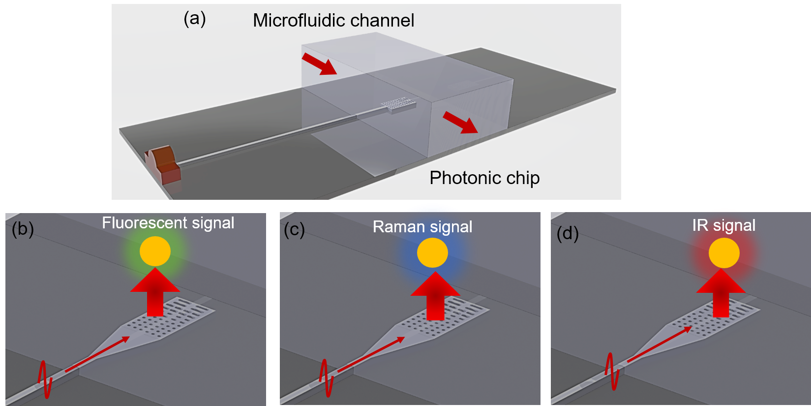
The research to date in terms of miniaturizing these techniques tends to focus more on developing hardware for on-chip “detection”. However, far too little attention is paid to on-chip hardware for “excitation”. Most of the existing work uses benchtop laser beams focused on the chip for excitation [8, 14]. A major disadvantage of this method is that photonic excitation is not spatially confined and results in high background noise, leading to poor signal-to-noise (SNR) ratio and sensitivity.
If we can develop a platform that can miniaturize the excitation and detection hardware on a small chip, it would offer a multitude of advantages. First, scaling up of the imaging field of view can be achieved by multiplexing a large number of excitation sources. Second, it provides compact hardware geometry to implement the setup at a low-cost with high volume production. Third, it offers opportunities to develop automated methods for biological analysis such as cell screening and probing.
Our planar photonic waveguide-based metasurface can enable miniaturized excitation sources which efficiently guide and manipulate photons on the chip. Researchers have previously demonstrated waveguides which guide and diffract light out of the plane using conventional grating surfaces. For example, Kerman et al used a conventional focused grating coupler design to excite samples in a microfluidic chip [18]. Such designs typically enhance fiber coupling in photonic integrated circuits [19-21]. However, these gratings employ a high degree of symmetry in their structure and so fail to a provide uniform collimated out of-the-plane excitation of the liquid sample flowing in an integrated microfluidic sensor channel. An artificial diffracting (meta) surface that can collimate the beam out of the plane uniformly over a wide area would greatly benefit on-chip microfluidic sensing [19,22-25], but meta-gratings today only focus on improving fiber to chip coupling.
In the present manuscript, we use an inverse design approach to obtain a metasurface based photonic grating structure that provides a wide collimated beam for on-chip optical excitation and detection [26-27] for bio-sensing applications. We present FDTD modeling, optimization, fabrication and demonstration of a meta collimator, and compare it with conventional grating coupling designs.
2 Meta Collimator Design, Modeling and Fabrication
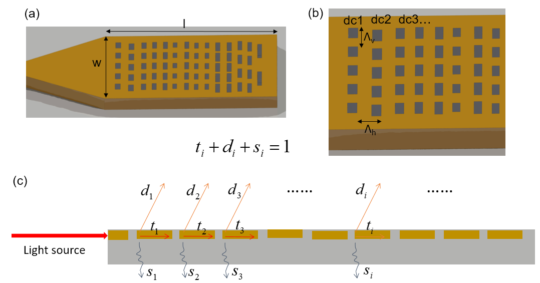
Conventional waveguide-based gratings have multiple identical diffracting grooves along the direction of light propagation that diffracts the photonic beam out-of-the-plane at a specified angle (Fig. 2c). However, the emission power of the light decreases exponentially as it progresses along the waveguide. To achieve uniform emission along the waveguide, we need to control the amount of energy diffracted from each individual diffracting groove, which is accomplished by engineering a unique distribution of light-scatterers along the direction of light propagation. We define rectangular light scattering grooves in the grating structure by their duty cycle (dc), row period () along the transverse direction, and line period (), as shown in Fig. 2b.
As a demonstration, we maintain the width, , and length, of the grating structure as 10 m and 20 m respectively (Fig. 2a). We optimize the distribution of scatterers to obtain uniform emission from the grating structure. The center wavelength of the emission spectrum is set to be in the C-band (1550 nm). Further, we ensure that the device can operate over a wide (70 nm) range of wavelengths while optimizing its structure for uniformity.
In our methodology, the optimization of the meta-grating is divided into two stages. The first optimization stage initializes the duty cycle of an individual row in the grating structure and then performs an iterative gradient descent inverse optimization to collimate the output beam. In general, gradient descent methodologies have many advantages. It allows us to optimize the photonic structure with relatively large degrees of freedom as compared to other gradient-free optimization schemes. Further, it requires fewer simulation steps and does not rely on parametric sweeps or random mathematical perturbations to find the optimum values.
2.1 Parameter Initialization
As the gradient descent method is highly sensitive to initial conditions, it is customary to initialize the parameters with relevant values. To come up with the initial values, we use an effective mirror model for the meta grating structure. The grating grooves can be approximated by the cascaded mirror model to understand the light propagation through the structure [28]. Fig. 2c shows the meta grating structure with its cascade mirror model. Transmission, diffraction, and scattering coefficients of the diffracting groove are assumed as , , and respectively. Diffraction intensity output from the first diffracting groove is proportional to , and is given by,
| (1) |
Using the cascaded mirror model, we can write intensity and in general are given by,
| (2) |
| (3) |
The collimated beam requires uniform emission from an individual groove. Mathematically, the condition is given by,
| (4) |
| (5) |
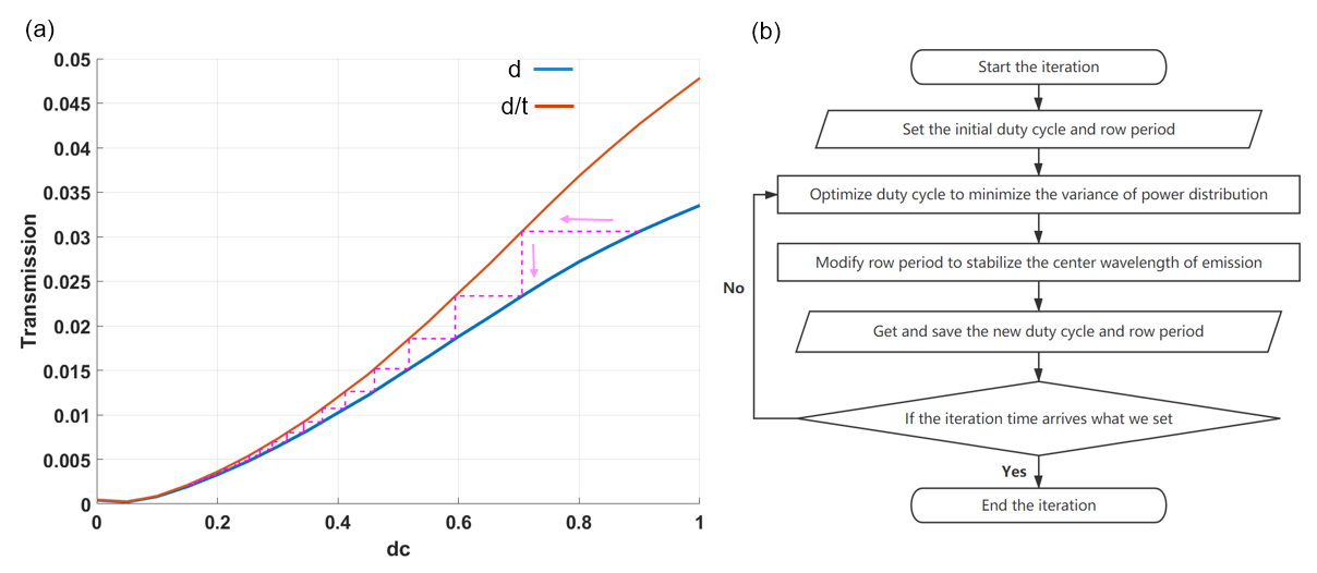
Assuming , the functions of the duty cycle, x and width w, of the groove. For constant width, we sweep the duty cycle and obtain the functions, and . Fig. 3a shows both the functions plotted for different values of the duty cycle, x.
Using the functions’ plot , we initialize the duty cycle for individual grating groove to satisfy the condition given by,
| (6) |
2.2 Iteration Method
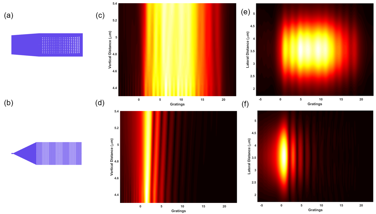
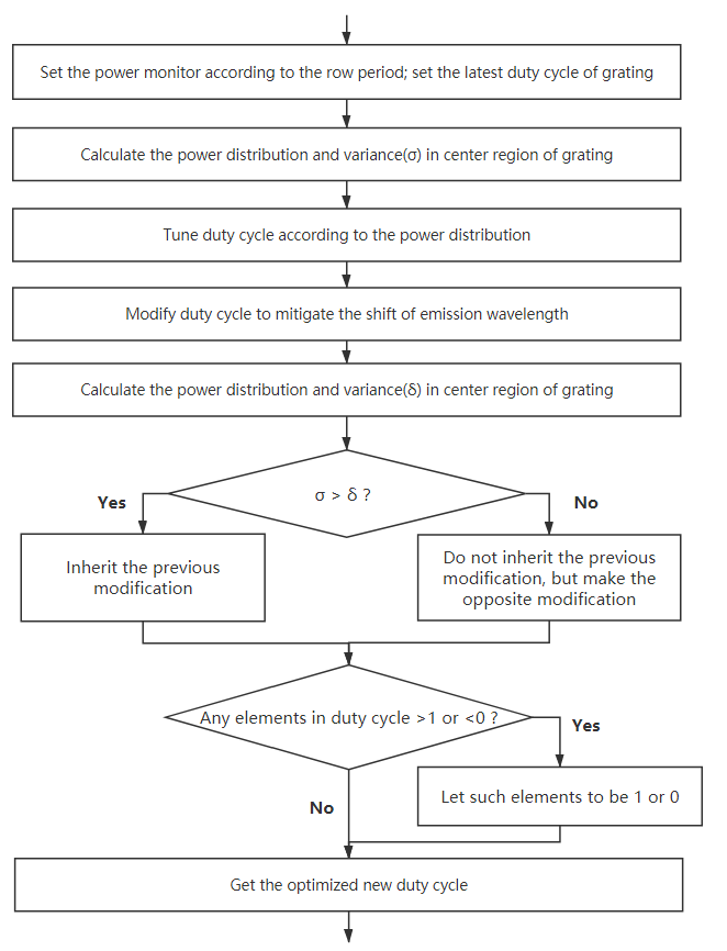
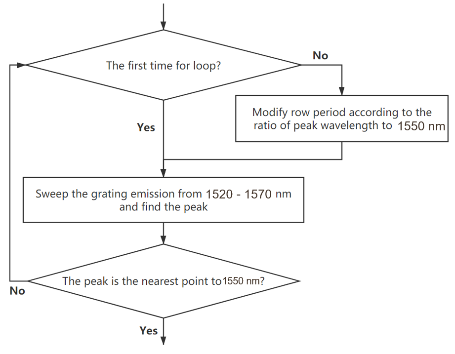
After the initialization process as explained above, we optimize the duty cycle of the individual grating groove in the meta-surface and obtain a collimated beam output. Lumerical FDTD software is used to perform the optimization which is based on the fact that the diffracted power from an individual groove increases with an increase in its duty cycle. We calculate the spatial distribution of diffracted power and its variance, then tune the duty cycle of each groove to minimize the variance. Fig. 3b shows the control flow chart of our iterative algorithm. With every iteration, the uniformity in the power distribution of the beam collimation increases. When the duty cycle and the grating period change, the effective index of the structure changes, as a result of which the center wavelength of grating emission also shifts. This may result in poor convergence of the duty cycle in the iterative procedure. Therefore, the central emission wavelength needs to be stabilized in the iterations by modifying the grating period. We add an additional step in our algorithm to tune the groove period () and stabilize the emission wavelength. Results obtained from the optimization process are shown in Fig 4. It shows the top and side view of the output beam from the optimized metasurface and compares it with a conventional binary grating structure.
After optimization, we get a collimated beam with up to 50nm of operating bandwidth. Besides, it should be noted that some spatial randomness is incorporated in each groove to avoid the lattice diffraction patterns in the profile. More details on the iterative procedure followed in the optimization can be found in the Appendix of the manuscript.
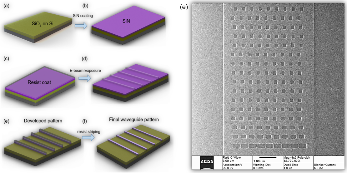
With the optimized design parameters, we fabricate the structures using the fabrication steps shown in Fig. 5. A low-pressure chemical vapor deposition (LPCVD) system is used to deposit 400 nm thick silicon nitride () layer on a 6-inch silicon dioxide wafer (3-micron oxide on Si substrate). These thermal oxide wafers are procured from Wafer Pro LLC, CA. The gratings and waveguides are then designed and patterned on silicon nitride on-insulator substrate via e-beam lithography and followed by reactive ion etching to define the geometry of the grating structures. Fluorine chemistry with a gas mixture of CHF3 and CF4 is used in the dry etching step. The leftover resist is stripped off using oxygen cleaning and acetone rinsing.
3 Design Performance and Characterization
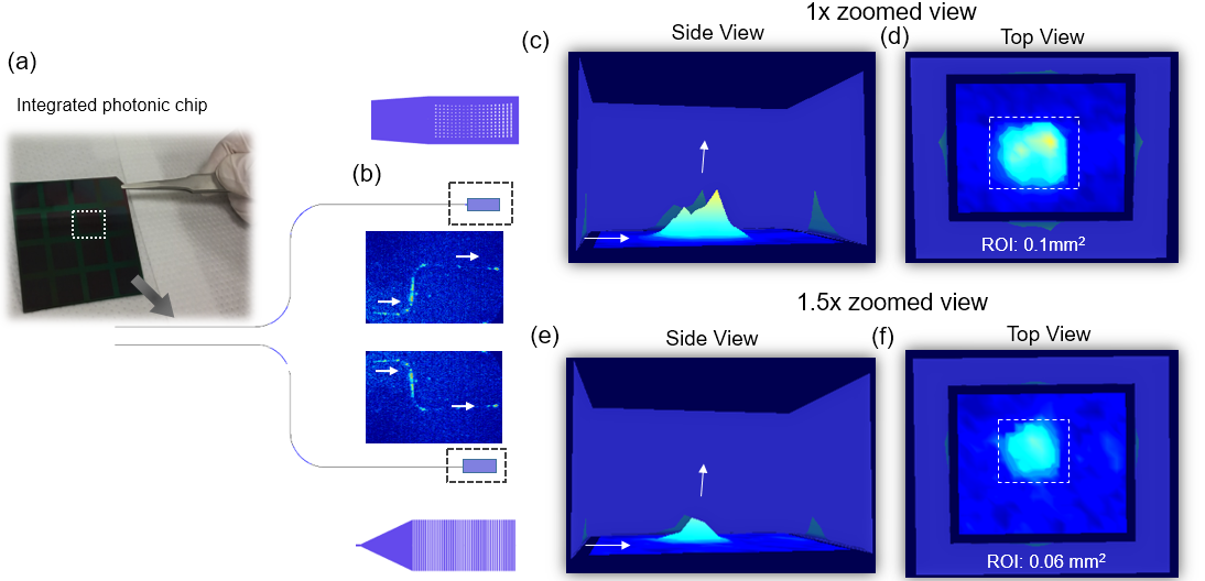
We benchmark the fabricated photonic meta-surface against a conventional binary grating-based diffractor. Fig. 6 shows the experimental analysis of the beam profile for the micro-structures. Please note that we display a 1.5x zoomed version of the beam profile from the conventional gratings for better visualization against the 1x version of the beam profile from the meta structure. During the experimental characterization, the CinCam InGasAS SWI camera (from Axiom Optics) is mounted upside down to analyze the beam. Fig 5b shows the microscopic view of the light propagating in the photonic waveguides. Fig. 6c and e compare the side view of the beam pattern, whereas the respective top views are shown in Figs. 6d and 6f. We find that the power delivered through the meta-surface is almost 1.4 times that of the conventional grating surface. The SNR of the illumination increased from 15 dB to 23 dB. The beam spot also improves from ROI of 0.06 mm2 to 0.1 mm2. Further, the homogeneity of the beam increases almost 2 times with the meta-surface enabling greater light illumination efficiency of the on-chip device.
4 Conclusion
In this manuscript, we demonstrate a meta-surface based photonic beam collimator for on-chip optofluidic probing. With renewed interest in developing chip-scale spectroscopic methods for sensing, the beam collimator would be an attractive option for miniaturized excitation sources. We adopt an inverse design strategy to optimize the meta structure. The optimization was based on a gradient descent method where the parameters were initialized using an effective mirror model. The designed meta-surface is successfully fabricated and experimentally characterized. We compare its beam profiling performance with a conventional binary grating structure. Such an excitation source when integrated with a planar waveguide-based photonic detector has the potential to miniaturize on-chip spectroscopy.
5 Appendix
We explain the optimization process in greater detail here. As stated earlier in the manuscript, the optimization parameters are the duty cycle and the grating period. The duty cycle optimization is explained in the flow chart given in Fig. 7. The flow chart for the row period optimization is shown in Fig. 8.
References
- [1] P. C. Wuytens, A. G. Skirtach, and R. Baets, “On-chip surface-enhanced Raman spectroscopy using nanosphere-lithography patterned antennas on silicon nitride waveguides,” Opt. Express, vol. 25, no. 11, p. 12926, 2017.
- [2] R. Baets et al., “Spectroscopy-on-chip applications of silicon photonics,” Integr. Opt. Devices, Mater. Technol. XVII, vol. 8627, p. 862701, 2013.
- [3] O.Yakar, Y.Nie, K.Wada, A.Agarwal and I.Ercan, “Energy Efficiency of Microring Resonator (MRR) Based Binary Decision Diagram (BDD) circuit,” IEEE International Conference on Rebooting Computing, 2019.
- [4] O. Graydon, “On-chip spectroscopy,” Nat. Photonics, vol. 12, no. 4, pp. 189–189, 2018.
- [5] R. Singh, P. Su, L. Kimerling, A. Agarwal, and B. W. Anthony, “Towards on-chip mid-infrared photonic aerosol spectroscopy,” Appl. Phys. Lett., vol. 113, no. 23, 2018.
- [6] A. C. Liapis, B. Gao, M. R. Siddiqui, Z. Shi, and R. W. Boyd, “On-chip spectroscopy with thermally tuned high-Q photonic crystal cavities,” Appl. Phys. Lett., vol. 108, no. 2, pp. 1–5, 2016.
- [7] R. Singh, D. Ma, L. Kimerling, A. M. Agarwal, and B. W. Anthony, “Chemical Characterization of Aerosol Particles Using On-Chip Photonic Cavity Enhanced Spectroscopy,” ACS Sensors, vol. 4, no. 3, pp. 571–577, 2019.
- [8] L. Pang, H. M. Chen, L. M. Freeman, and Y. Fainman, “Optofluidic devices and applications in photonics, sensing, and imaging,” Lab Chip, vol. 12, no. 19, pp. 3543–3551, 2012.
- [9] R. Singh, D. Ma, A. Agarwal, and B. Anthony, “On-chip photonic particle sensor,” vol. 1049112, no. February 2018, p. 37, 2018.
- [10] A. Dhakal, P. Wuytens, F. Peyskens, A. Z. Subramanian, N. Le Thomas, and R. Baets, “Silicon-nitride waveguides for on-chip Raman spectroscopy,” Opt. Sens. Detect. III, vol. 9141, p. 91411C, 2014.
- [11] P. C. Wuytens, A. G. Skirtach, and R. Baets, “On-chip surface-enhanced Raman spectroscopy using nanosphere-lithography patterned antennas on silicon nitride waveguides,” Opt. Express, vol. 25, no. 11, p. 12926, 2017.
- [12] R. Singh, “Whispering photons : on-chip biophotonic integrated circuits for point-of-care diagnostics,” Thesis: S.M., Massachusetts Institute of Technology, Department of Mechanical Engineering, 2018.
- [13] G. Persichetti, I. A. Grimaldi, G. Testa, and R. Bernini, “Multifunctional optofluidic lab-on-chip platform for Raman and fluorescence spectroscopic microfluidic analysis,” Lab Chip, vol. 17, no. 15, pp. 2631–2639, 2017.
- [14] H. Takehara et al., “On-chip cell analysis platform: Implementation of contact fluorescence microscopy in microfluidic chips,” AIP Adv., vol. 7, no. 9, 2017.
- [15] J. W. Dobrucki and U. Kubitscheck, “Fluorescence Microscopy,” Fluoresc. Microsc. From Princ. to Biol. Appl. Second Ed., vol. 2, no. 12, pp. 85–132, 2017.
- [16] J. Chen, J. Abell, Y. W. Huang, and Y. Zhao, “On-chip ultra-thin layer chromatography and surface-enhanced Raman spectroscopy,” Lab Chip, vol. 12, no. 17, pp. 3096–3102, 2012.
- [17] F. Peyskens, P. Wuytens, A. Raza, P. Van Dorpe, and R. Baets, “Waveguide excitation and collection of surface-enhanced Raman scattering from a single plasmonic antenna,” Nanophotonics, vol. 7, no. 7, pp. 1299–1306, 2018.
- [18] S. Kerman et al., “Integrated Nanophotonic Excitation and Detection of Fluorescent Microparticles,” ACS Photonics, vol. 4, no. 8, pp. 1937–1944, 2017.
- [19] R. Marchetti et al., “High-efficiency grating-couplers: Demonstration of a new design strategy,” Sci. Rep., vol. 7, no. 1, pp. 1–8, 2017.
- [20] L. A. Weller-Brophy and D. G. Hall, “Waveguide Diffraction Gratings In Integrated Optics,” Integr. Opt. Circuit Eng. II, vol. 0578, no. May, p. 173, 2012.
- [21] B. J. Offrein, G.-L. Bona, R. Germann, I. Massarek, M. M. Spuhler, and D. Erni, “A very short planar silica spot-size converter using a nonperiodic segmented waveguide,” J. Light. Technol., vol. 16, no. 9, pp. 1680–1685, 2002.
- [22] A. Michaels and E. Yablonovitch, “Inverse Design of Near Unity Efficiency Perfectly Vertical Grating Couplers,” Opt. Express, vol. 26, no. 4, pp. 2614–2617, 2017.
- [23] N. V. Sapra et al., “Inverse Design and Demonstration of Broadband Grating Couplers,” IEEE J. Sel. Top. Quantum Electron., vol. 25, no. 3, 2019.
- [24] S. Molesky, Z. Lin, A. Y. Piggott, W. Jin, J. Vucković, and A. W. Rodriguez, “Inverse design in nanophotonics,” Nat. Photonics, vol. 12, no. 11, pp. 659–670, 2018.
- [25] J. Jiang, J. Cai, G. P. Nordin, and L. Li, “Parallel micro genetic algorithm design for photonic crystal and waveguide structures,” Opt. Lett., vol. 28, no. 23, p. 2381, 2007.
- [26] L. F. Frellsen, Y. Ding, O. Sigmund, and L. H. Frandsen, “Topology optimized mode multiplexing in silicon-on-insulator photonic wire waveguides,” Opt. Express, vol. 24, no. 15, p. 16866, 2016.
- [27] B. Shen, P. Wang, R. Polson, and R. Menon, “Ultra-high-efficiency metamaterial polarizer,” Optica, vol. 1, no. 5, p. 356, 2014.
- [28] Larry Coldren and Scott Corzine, “Diode Lasers and Photonic Integrated Circuits,” https://doi.org/10.1002/9781118148167.ch3.