Spin coating TPB film on acrylics and measurement of its wavelength shifting efficiency
Abstract
Scintillation light from liquid noble gas in a neutrino or dark matter experiment lies typically within the vacuum ultraviolet (VUV) region and might be strongly absorbed by surrounding materials such as light guides or photomultiplier. Tetraphenyl butadiene (TPB) is a fluorescent material and acts as a wavelength shifter (WLS) which can turn the UV light to the visible light around a peak wavelength of 425 nm, enabling the light signals to be detected easily for physics study. Compared with a traditional TPB coating method using vapor deposition, we propose an alternative technique with a spin coating procedure in order to facilitate the development of neutrino and dark matter detectors. This article introduces how to fabricate the TPB film on acrylics using the spin coating method, reports measurement of sample film thickness and roughness, shows the reemission spectrum, and quantifies the wavelength shifting efficiency (WLSE).
I Introduction
Wavelength shifter (WLS) is critical in modern liquid noble gas detectors. It shifts ultraviolet light signal to visible light signal of particular wavelength. The wavelength of scintillation light form liquid noble gas is vacuum ultraviolet (VUV) varying from 80 nm to 200 nm. Light in this wavelength range would be strongly absorbed by most detector materials. Tetraphenyl butadiene (TPB) is among one of the favorite WLS options Benson:2017vbw ; Kuzniak:2018dcf ; Poehlmann:2018sto in a number of neutrino and dark matter experiments using liquid argon, such as MicroBooNE Fleming:2012gvl , DUNE Abi:2018alz , DEAP-3600 b15 ; b5 , DarkSide-20k Aalseth:2017fik and ArDM Amsler:2010yp , which absorbs UV light and re-emit lights in visible spectrum to be easily and effectively detected by photomultipliers tubes (PMT) or Silicon Photomultipliers (SiPM). WLS is also used in Cherenkov detectors to improve light yield Dai:2008cp ; Sweany:2011qh ; Joosten:2016lcl . It is of important value for current and next-generation experiments to find a cost-effective way to coat the TPB on the surface of detector container.
A vapor deposition method Bonesini:2018ubd is commonly used in TPB film fabrication, and the reference Howard:2017dqb proposes a spraying method. Since the vapor deposition method asks for the high vacuum and spraying method has no control on the film thickness, we propose a fabrication of TPB film using the spin-coating method, which can act as an alternative option. The primary purpose of this study is to make TPB films using the spin coating method and measure the film geometry as well as its capability of shifting UV lights. The light shifting capability of the TPB material is quantum efficiency (QE), which is defined as average number of photons TPB reemits when it absorbs a single photon. QE is an intrinsic property of the material itself and is independent of the film condition, e.g. thickness and roughness. Since it is hard to obtain a single photon as incident light, it is difficult to measure QE directly. Therefore, the shifting capability of the whole film under multiphoton incident light, which is called wavelength shifting efficiency (WLSE), is measured instead. WLSE turns out to be a result of folding QE with the film condition and the optical configuration. It is a more straightforward representation of TPB film performance in physics applications.
Although UV light from most of liquid noble gas has a wavelength below 200 nm and cannot even transport much longer distance in air or acrylic, the reference Benson:2017vbw shows a clear relationship of WLSE with incident light at different wavelengths. The WLSE at different wavelengths share similar trends when they vary with the film thickness Francini:2013lua . This enables us to perform our WLSE measurement at a selected wavelength of 254.5 nm, even without vacuum environment. TPB is known to form at least four polymorphic types of crystals, depending the deposition method CEC2014 ; LPR2014 . The optical response at 250 nm including the absorption and in consequence the WLSE of these different types of TPB can be quite different CG2010 . It is also known that the scinillation yield of macroscopic TPB crystals grown from solution is much higher than the yield of evaporated coatings IEEE2009 ; Pollmann:2010gs . Despite differences in the deposition method, it is assumed that the main results will still hold in the same way.
In this study, we first propose a different TPB coating technique in Sec. II. Then we describe the experimental setup to measure the optical properties from our TPB samples in Sec. III. An analysis method follows, in Sec. IV, to quantify the WLSE with an emphasis on geometrical acceptance ratio corrections. In Sec. V, we report the light reemission spectrum by our TPB samples and make a comparison of WLSE between our results and those reported in the recent study. Finally, we come to the summary and conclusion.
II Fabrication with Spin Coatings
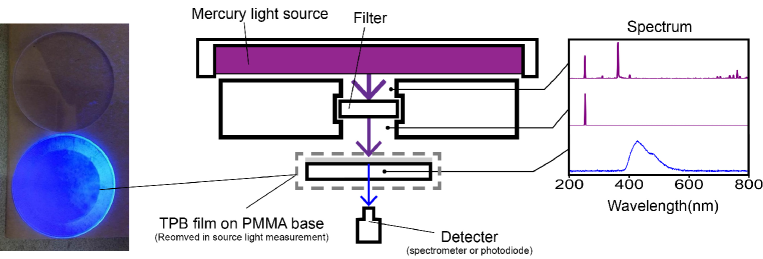
Without a loss of generality, we choose an acrylic disk as the base material for a demonstration of TPB coatings due to its high transparency in the interesting wavelength region. A description of the spin coating procedure is shown in Fig. 1.
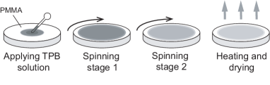
Methylbenzene was used as the solvent for the TPB powder, as its capability has been given in the literature solvant . According to the study in the literature liyan , the spinning speed was the major factor affecting the thickness of the film while the duration does not matter much.
We first sanded the surface of acrylics and applied the TPB solution with the methylbenzene as our solvent to the target surface. Then the TPB solution spreaded in stage 1 and the solvent methylbenzene volatilizes in stage 2, according to the previous study b18 ; b21 . In this way, Stage 1 affects the thickness of the film the most as TPB was carried in the spilled solution. We performed preparative experiments to find the proper speed and the duration for stage 1. The solution barely spills in stage 2 due to its viscosity and the sample thickness would no longer change any more, which allows us to choose parameters for stage 2 based on experience without a loss of generality.
The solubility of TPB in methylbenzene was roughly around 0.021 g/ml by means of weight measurement in the room temperature. The concentration of 0.02 g/ml was chosen for the fabrication of samples. The acrylic substrate in the round shape was fixed on the spinning-platform of the spin coating machine by a vacuum pump. TPB solution was added to the center of the acrylic disk manually. The spinning process consists of two stages with different speed and duration. Various combinations of speed and duration are used in a preparative experiment. The key parameters to prepare samples in the spin coating procedure are summarized in Table 1.
| Stage one | speed | 700 r/min |
|---|---|---|
| duration | 6 s | |
| Stage two | speed | 1000 r/min |
| duration | 20 s | |
| concentraion | 0.02 g/ml |
After the spinning procedure, the sample was placed on a heated table at 70∘C for 2 minutes to get dried. As an experience from experiment, the temperature and duration might not matter much as long as the film was completely dried.
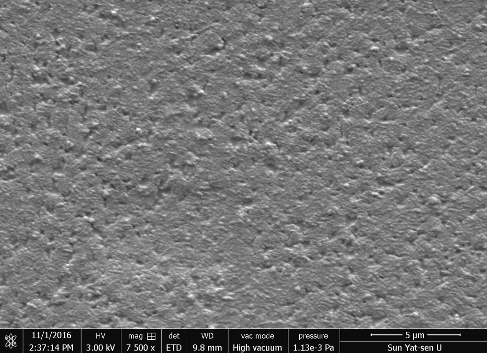
The fabricated sample looks rather uniform and stable based on finger touches. Further surface measurements by SEM were performed and given in Fig. 2 111The measurement was done in Nov. 1, 2019. The raw SEM picture had a wrong date due to the software.. We saw tiny holes, which might be caused by the fast heating and drying processes. The more uniformly the TPB film is fabricated, the better the fabrication method will be applied in the particle experiments. It deserves further investigation of temperature and cure to improve the surface roughness. Samples were preserved in dark environment to prevent degradation Chiu:2012ju ; Jones:2012hm .
We then measured the thickness and roughness of different TPB films made by the spin-coating method. A profilometer was used for our purpose. Each sample was scratched by a piece of metal to create a notch as the requirement of profilometer.
.
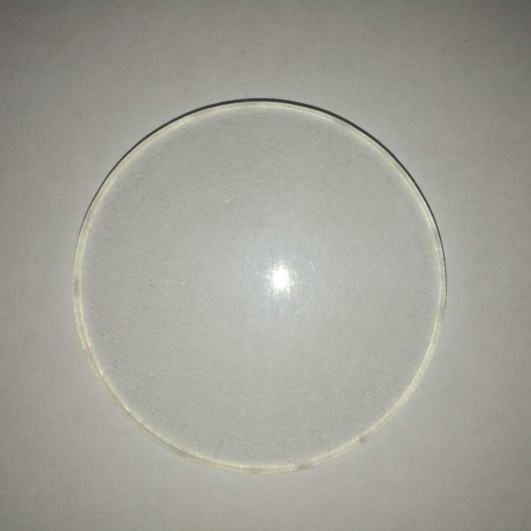
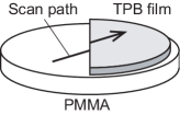
The left panel in Fig. 3 is a photo of an acrylic disk coated with the TPB film. A special kind of samples, which have only half of their surface covered by the TPB film, shown in the right panel of Fig. 3, were made for the purpose of roughness and thickness measurement. These special samples were made using the same parameter in the fabrication process except half of their surfaces were protected by a blank paper film before the TPB solution was added. The paper film was removed after the TPB solvent was completely dried. It was assumed that this half-pearl paper film would not affect the thickness and roughness of TPB film. Fig. 4 shows scanning results of a TPB half-coated film and a scratched film done by a profilometer. Each scan covered a 4 mm long path and provided the height along the path. It is then safe to consider the result on these paths representing the properties of the whole film because the film is almost uniformly distributed b16 . The peak at the boundary in the TPB half-coated sample was caused by the protection film used in the fabrication process. We consider this accumulation as the result of wet edge between the solution and the final film, and assume that the edge does not affect the TPB-coated area far from the boundary. Thus this peak would be ignored in the following steps.
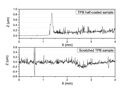
In the result of a half-coated sample, the profilometer scan path covered an edge of the TPB film so that both surfaces of the TPB film and the acrylic substrate were included. The average height of the coated part with respect to the substrate was considered as the thickness and the uncertainties in a measurement of the unscratched part was considered as a representation of roughness. The measurements had been repeated several times, as results are shown in Table 2. The scans for scratched samples used a path of 4 mm each time as well. The obvious valley represents the scratch we made on purpose. The difference between the bottom of the valley and the baseline is considered as the thickness of this sample.
| measurements | thickness() | roughness() |
|---|---|---|
| 1 | 0.15 | 0.051 |
| 2 | 0.17 | 0.100 |
| 3 | 0.22 | 0.074 |
| 4 | 0.19 | 0.081 |
| average | 0.18 | 0.076 |
As shown in Table. 2, the thickness of TPB fabricated by the spin coating method was thinner than the reported result made by the vapor deposition. Therefore, it was expected that the WLSE here was slightly lower than the thicker sample produced by the vapor deposition.
III Experimental Setup
All apparatus used in experiment are listed in Table 3. A custom apparatus setup was built for measurements of spectrum and photocurrent. A schematics of this setup is shown in Fig. 5.
| Apparatus | Type |
|---|---|
| Spectrometer | Ocean 2000ocean |
| Profilometer | KOSAKA ET150kosaka |
| UV light | WFH-204bwfh |
| The filter | Shengyakang |
| Si Photodiode | LXD-66MQ |
| Spinner | KW-4AKW |
| Voltmeter | DM3000 Seriesdm |
We take a mercury lamp with filter installed right in front of the light exit window as the light source. The lamp provides lights ranging from 245 nm to 405 nm according to the characteristic spectrum of mercury. The spectrum of source light and reemission light overlaps at the wavelength of around 400 nm to 420 nm, which hinders our optical measurement. Therefore, a second filter, an interference filter with transmission peak at a wavelength of 254.5 nm was introduced to generate the monochromatic incident light.
From now on, the upper surface of filter or the TPB film are considered as light sources. The spectrum measurements of both incident light and reemission light are done by a fiber spectrometer. The entrance of the fiber was placed at a fixed position and angle. Counting the photocurrent was done by a silicon photodiode. Due to the strong absorption of UV light in the air, the light sensor, i.e. the photodiode or the fiber entrance, was placed as close to the light source as possible. It means that the detector touches either the lower surface of filter or the acrylic substrate.
A DC power supply at 5 V was supplied to the Silicon photodiode set to work in the photoconductive mode, which was not compulsory but could slightly improve photocurrent measurements. The photodiode had been calibrated by its vendor. This spectrometer covered the range from 200 nm to 800 nm. The fiber was supposed not to bring systematic uncertainties after a careful calibration. During data taking in each measurement, ambient noise in the lab environment was measured and subtracted with the help of a control and analysis software. In principle, two configurations in the optical measurement have slightly different geometries. The geometry-related correction have been considered in our analysis later.
IV Analysis methods
WLSE is defined as the ratio between the reemission light intensity and the incident light intensity produced by the coated film. We first establish an optical model to help with the data analysis. For a monochromatic light at a wavelength of , each photon with energy of would cause the photocurrent of , where is the response of photodiode handbook . Hence, the number of photons can be calculated with the photocurrent in the following equation:
| (1) |
Given a continuous light spectrum of (a normalized factor), this equation can be transformed into the following:
| (2) |
Hence the WLSE would be:
| (3) |
where A is a geometrical acceptance ratio which represents, roughly, the geometrical difference of apparatus configurations used to measure and . The numerical value for the ratio of two integrals in the middle of Eqn. (3) is 0.96. In general, we need to measure photocurrent , using photodiode, and spectrum , by a fiber spectrometer. In order to measure the photocurrent of the light source, on one hand, the TPB film was removed and the filter surface was considered as our light source. On the other hand, during a measurement of the reemission photocurrent, the TPB film was considered as the light source. The photodiode was placed as close to the light source as possible in each measurement. Thus the distance between a photodiode and a light source shall be determined by the thickness of the acrylics or filter. Since the filter was thinner, the Si photodiode received more light in light source measurement because it was indeed closer to the light source. A geometrical acceptance ratio was introduced to take the difference into account and make our measurements more accurate and self-consistent. This factor was determined by the geometry of apparatus configurations, which was simplified into the model shown in Fig. 6 by means of geometrical optics.
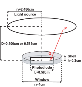
Among dimensions marked in Fig. 6, and were measured in the laboratory with a precision of 0.01 mm while was provided by its vendor. These values will be taken into account during error propagations. Although the uncertainty in was not provided, we took a conservative uncertainty at 0.2 mm. The other parameters such as and were also measured by micrometer but ignored in the error propagation, because it turned out that their influence would be less than 0.1% in our estimation. In a short summary, uncertainties of , and were considered and would be processed for further quantitative analysis.
Both source light and reemission light are considered as an even circular area Lambert source with the same size. The silicon photodiode has a square-shape sensitive area. Suppose that P is a point on the area light source and Q is a point on photodiode. The intensity of light, measured by luminous flux, received by Q would decrease if Q is far from P or deviate from the exact front of P, for lambert light source, Q would be receiving luminous flux of:
| (4) |
where , is a surface element near P and Q, respectively. B represents the brightness. Since we are interested in their ratio, it is safe to take the brightness B as 1.
In terms of the reemission light, there are two major factors that could reduce the intensity of light. Firstly, there is a reflection when light enters the surface of the acrylic disk. Here we will ignore multiple reflections so that the reflected light will simply be lost. Secondly, light will be attenuated exponentially in acrylics. However, the acrylic substrate is very thin while the light attenuation length in acrylics at 420 nm is more than one meter according to the previous measurement attenuation_length . It means that the attenuation effect will be extremely weak. A simple estimate will tell us that the difference caused by an exponential attenuation should be less than 0.5%. Therefore, the attenuation effect can be safely ignored here. In conclusion, an extra reflection factor has to be included to describe a reduction of light intensity due to reflections on acrylics. The transmission factor remains the same when swapping index 1 and 2 in Eqn. (6). Then will be simply factored in twice.
| (5) |
where
| (6) |
The transmission factor is calculated according to the Fresnel formula, assuming that incident light was not polarized there with equal contributions from P-wave(parallel) and S-wave(transverse). The calculation requires two refractive indices from the air and the acrylics: and based on the work refractive_index . Fig. 7 shows how the reflection factor varies with the angle of incident light.

It is necessary to integrate over the surface P and Q to get the ratio of light intensity at the source and the light intensity received by photodiode:
| (7) |
Note that the transmission factor only appears in reemission light measurement. is the total intensity at the light source, which has the same value in two setups and thus would be canceled each other in the ratio. The boundary of (, ) and (, ) is circle and square respectively , with dimensions shown in Fig. 6. Parameter D is 0.300 cm for the source light measurement, and 0.583 cm for the reemission measurement. Note that the shell of photodiode could possibly block the light. This situation was cross checked and safely treated in the integral. This integral is then calculated numerically. The parameter G represents a light detection efficiency of photodiode. The geometrical acceptance ratio A for different setups is given by:
| (8) |
We immediately calculated results for and . After that, we then obtain the geometrical acceptance ratio at 0.848. This value is smaller than 1, indicating that the photodiode is less likely to receive reemission light than source light, and this is mainly because the acrylic surface reflects the reemission light. As the light source is much larger than the photodiode, this factor is not sensitive to a horizontal movement of the photodiode, which provides a high tolerance for the deviation of photodiode placement by hand. As mentioned above, the geometrical acceptance ratio A is determined by , and . Errors on measured values will be propagated in the results eventually.
V Results
| Index(i) | Name | Stdev() | Precision() | () | Measuring times |
|---|---|---|---|---|---|
| 1 | 8.394 | 0.0001 mV | -0.00074 | 23 | |
| 2 | 0.075 | 0.0001 mV | 0.00074 | 5 | |
| 3 | 1.881 | 0.0001 mV | 0.0033 | 24 | |
| 4 | 0.108 | 0.0001 mV | -0.0033 | 6 | |
| 5 | 0.01 mm | 0.042 | 1 | ||
| 6 | 0.2 mm | -0.049 | 1 | ||
| 7 | 0.2 mm | -0.0054 | 1 |
V.1 Photocurrent and spectra
The spectra of incident light and reemission light are shown in Fig. 8. The reemission spectrum matches the result reported in Ref. Benson:2017vbw , which indicates that the solvent and coating process would not affect TPB properties.
These spectrum will be used in calculation of WLSE.
A 100 k resistor is connected to the photodiode in series to read out the photocurrent as voltage. Note that this resistor value would be canceled in ratio so that it would not contribute to uncertainties in the end. We actually replace the photocurrent with the generated voltage signal in Eqn. (3) to avoid measuring the resistor which brings an extra uncertainty.
To guarantee validity of our results, photocurrent measurements of the light source and the TPB reemission were carried out in 6 times and 11 times, respectively. UV light source was turned off between each measurement to avoid photodiode temperature rise which would further affect photocurrent. Photocurrent is 341.88.4 mV labeled as in the source light measurement and 79.61.9 mV in the reemission measurement labeled as , where the error is standard deviation. Dark current is 4.10.1 mV labeled as in the source light measurement and 4.80.1 mV labeled as in the reemission measurement, respectively. Dark current is then subtracted in the analysis.
V.2 Uncertainties
As mentioned above, we have to consider the uncertainty of WLSE propagated from voltage signals and geometric measurements. For voltage measurements, on one hand, we have to include incident light voltage, reemission light voltage and their respective dark counts. The precision of voltmeter we used goes to the level of 0.0001 mV. The statistical uncertainty comes from the standard deviation of light voltage with its own dark voltage subtracted. The systematic error is calculated according to the precision of our voltmeter. The partial derivatives WLSE with respect to these values will then be calculated analytically. For geometric measurements, on the other hand, we also use standard deviations as statistical errors and calculate systematic errors from the precision by micrometer. Note that these values take part in the numerical integral Eqn. (7). Thus, the partial derivatives WLSE will be calculated numerically.
We present a list of uncertainties in Table. 4 which covers all values we measured with their precisions and standard deviations(Stdev). The notation for each value is defined there as well. If we define the combined statistical uncertainty with as its degrees of freedom and the systematic uncertainty with as its degrees of freedom, we can list the formula and results in error propagations as follows:
| (9) |
| (10) |
| (11) |
| (12) |
| (13) |
| (14) |
We check the coverage factor and the corresponding degrees of freedom from the t-distribution table nist . The uncertainty of WLSE can be obtained as WLSE = at the 95 % confidence level (C.L.).
V.3 WLSE
The result of WLSE based on our TPB samples is on average at 95 % C.L. This result is in line with the trend of measurements in Ref. Benson:2017vbw , where the WLSE of a 0.7 m TPB film is around m (thickness of our samples are around 0.18 m shown in Table. 2). Recalling that WLSE as a property of the film, is determined by intrinsic property of TPB material, QE, and the optical setup. It is, therefore, reasonable to expect that WLSE here would become lower as the film is thinner.
VI conclusions
We have successfully fabricated stable and well-functioning TPB films on acrylic disks by the spin coating method. We have measured those samples that thickness of the film is around 182 nm, and the surface was proven to be rather uniform by means of SEM. We have established an experimental setup to measure the optical properties of TPB films. We have checked TPB reemission spectrum, which perfectly matches the result reported in the previous work Benson:2017vbw . The WLSE in our samples has reached % at 95% C.L. as the similar level of TPB samples prepared by the vapor deposition method. The preliminary results show the feasibility of the spin coating techniques, though mass productions ask for more research and development. Tuning parameters in the spin coating procedure will likely increase the WLSE and meet requirements of different experiments. One of shortcomings in the spin coating method remains how to deal with large panels without a round shape. Current commercial instruments cannot be applied any more. However, it is the relative velocity between the TPB liquid solution and the substrate to meet physics requirements. In the large scale applications, we might have to spill the liquid solution onto the surface by adapting well-designed jigs and heaters to fit the detector with a particular geometry. We will also have to elaborate the procedure in the clean room in the near future to avoid radioactive backgrounds which hinders the current technology in DM and neutrino experiments. We expect this simple WLS coating technique to be optimized for future neutrino and dark matter detector constructions.
VII Acknowledgement
This work was strongly supported by the Center for Fundamental Physics Laboratory in SYSU. We appreciate great help from Prof. Han Shen and technicians in his team. Many thanks to Prof. Yue Zheng and Prof. Wen-Peng Zhu’s help for sample measurements by SEM.
References
- (1) C. Benson, G. Orebi Gann and V. Gehman, “Measurements of the intrinsic quantum efficiency and absorption length of tetraphenyl butadiene thin films in the vacuum ultraviolet regime,” Eur. Phys. J. C 78, no. 4, 329 (2018) [arXiv:1709.05002 [physics.ins-det]].
- (2) M. Kuzniak, B. Broerman, T. Pollmann and G. R. Araujo, “Polyethylene naphthalate film as a wavelength shifter in liquid argon detectors,” Eur. Phys. J. C 79, no. 4, 291 (2019) [arXiv:1806.04020 [physics.ins-det]].
- (3) D. M. Poehlmann, D. Barker, H. Chagani, P. Cushman, G. Heuermann, A. Medved, H. E. Rogers and R. Schmitz, “Characterization of Gadolinium-loaded Plastic Scintillator for Use as a Neutron Veto,” arXiv:1812.11267 [physics.ins-det].
- (4) B. Fleming [MicroBooNE Collaboration], “The MicroBooNE Technical Design Report,” doi:10.2172/1333130
- (5) B. Abi et al. [DUNE Collaboration], “The DUNE Far Detector Interim Design Report, Volume 2: Single-Phase Module,” arXiv:1807.10327 [physics.ins-det].
- (6) B. Broerman et al., “Application of the TPB Wavelength Shifter to the DEAP-3600 Spherical Acrylic Vessel Inner Surface,” JINST 12, no. 04, P04017 (2017) [arXiv:1704.01882 [astro-ph.IM]].
- (7) P.-A. Amaudruz et al. [DEAP-3600 Collaboration], “Design and Construction of the DEAP-3600 Dark Matter Detector,” Astropart. Phys. 108, 1 (2019) [arXiv:1712.01982 [astro-ph.IM]].
- (8) C. E. Aalseth et al., “DarkSide-20k: A 20 tonne two-phase LAr TPC for direct dark matter detection at LNGS,” Eur. Phys. J. Plus 133, 131 (2018) doi:10.1140/epjp/i2018-11973-4 [arXiv:1707.08145 [physics.ins-det]].
- (9) C. Amsler et al. [ArDM Collaboration], “First results on light readout from the 1-ton ArDM liquid argon detector for dark matter searches,” JINST 5, P11003 (2010) [arXiv:1009.3641 [physics.ins-det]].
- (10) X. Dai, E. Rollin, A. Bellerive, C. Hargrove, D. Sinclair, C. Mifflin and F. Zhang, “Wavelength Shifters for Water Cherenkov Detectors,” Nucl. Instrum. Meth. A 589, 290 (2008) [arXiv:0807.2895 [physics.ins-det]].
- (11) M. Sweany, A. Bernstein, S. Dazeley, J. Dunmore, J. Felde, R. Svoboda and M. Tripathi, “Study of wavelength-shifting chemicals for use in large-scale water Cherenkov detectors,” Nucl. Instrum. Meth. A 664, 245 (2012) [arXiv:1110.3335 [physics.ins-det]].
- (12) S. Joosten, E. Kaczanowicz, M. Ungaro, M. Rehfuss, K. Johnston and Z.-E. Meziani, “Enhanced UV light detection using a p-terphenyl wavelength shifter,” Nucl. Instrum. Meth. A 870, 110 (2017) [arXiv:1611.03467 [physics.ins-det]].
- (13) M. Bonesini et al., “An innovative technique for TPB deposition on convex window photomultiplier tubes,” JINST 13, no. 12, P12020 (2018) [arXiv:1807.07123 [physics.ins-det]].
- (14) B. Howard et al., “A Novel Use of Light Guides and Wavelength Shifting Plates for the Detection of Scintillation Photons in Large Liquid Argon Detectors,” Nucl. Instrum. Meth. A 907, 9 (2018) [arXiv:1710.11233 [physics.ins-det]].
- (15) R. Francini et al., “VUV-Vis optical characterization of Tetraphenyl-butadiene films on glass and specular reflector substrates from room to liquid Argon temperature,” JINST 8, no.8, P09006 (2013). arXiv:1304.6117 [physics.ins-det].
- (16) A. Bacchi, A. Brillante, D. Crocco, et al., “Exploration of the polymorph landscape for 1,1,4,4-tetraphenyl-1,3-butadiene”, CrstEngComm, 2014, 16, 8205.
- (17) Andrea Camposeo, Marco Polo, Pompilio Del Carro, Leonardo Silvestri, Silvia Tavazzi and Dario Pisignano, “Random lasing in an organic light-emitting crystal and its interplay with vertical cavity feedback”, Laser Photoinics Rev. 8, No.5, 785-291 (2014).
- (18) Alberto Girlando, Sandra Ianelli, Ivano Bilotti, et al., “Spectroscopic and structural characterization of two polymorphs of 1,1,4,4-Tetraphenyl-1,3-butadiene”, Crystal Growth and Design, 2010, 10, 2752-2758.
- (19) Guiulia Hull, Natalia P. Zaitseva, Nerine J. Cherepy, et al., “New organic crystals for pulse shape discrimination”, IEEEE Trans. Nucl. Sci. 56, 899 (2009).
- (20) T. Pollmann, M. Boulay and M. Kuzniak, “Scintillation of thin tetraphenyl butadiene films under alpha particle excitation,” Nucl. Instrum. Meth. A 635, 127 (2011) doi:10.1016/j.nima.2011.01.045 [arXiv:1011.1012 [physics.ins-det]].
- (21) Z. Moss, L. Bugel, G. Collin, J. M. Conrad, B. J. P. Jones, J. Moon, M. Toups and T. Wongjirad, “Improved TPB-coated Light Guides for Liquid Argon TPC Light Detection Systems,” JINST 10, no. 08, P08017 (2015) doi:10.1088/1748-0221/10/08/P08017 [arXiv:1410.6256 [physics.ins-det]].
- (22) LI Yan, Pan Qing-Yi et al., “Preparation Prcoess of Nanosized Organic/Inorganic Thin films by Sol-Gel Spin-coating Method”. Journal of Inorganic Materials, 2004, Vol. 19, No. 5.
- (23) Dietrich Meyerhofer, “Characteristics of resist films produced by spinning”. Journal of Applied Physics 49, 3993 (1978).
- (24) YUE Hongda , PAN Longfa , XU Duanyi, “Evaporation and flow in the dye coating process”. J. Tsinghua Univ. (Sci&Tech), 2014, Vol. 44, No. 2.
- (25) C. S. Chiu, C. Ignarra, L. Bugel, H. Chen, J. M. Conrad, B. J. P. Jones, T. Katori and I. Moult, “Environmental Effects on TPB Wavelength-Shifting Coatings,” JINST 7, P07007 (2012) [arXiv:1204.5762 [physics.ins-det]].
- (26) B. J. P. Jones, J. K. VanGemert, J. M. Conrad and A. Pla-Dalmau, “Photodegradation Mechanisms of Tetraphenyl Butadiene Coatings for Liquid Argon Detectors,” JINST 8, P01013 (2013) doi:10.1088/1748-0221/8/01/P01013 [arXiv:1211.7150 [physics.ins-det]].
- (27) Alfred G. Emslie, Francis T. Bonner, and Leslie G. Peck, “Flow of a Viscous Liquid on a Rotating Disk”. Journal of Applied Physics 29, 858 (1958).
- (28) https://oceanoptics.com/product/usb2000-custom/
- (29) https://www.kosakalab.co.jp/english/product/precision/minute/
- (30) http://www.cit17.com/cit17_Product_2056126605.html
- (31) http://setcas.com/?page_id=890
- (32) https://www.rigolna.com/products/digital-multimeters/dm3000/
- (33) Shen Zhen Long Xin Da Technology Electronic Co., Ltd, “Si Photodiode - LXD-66MQ Hand Book”, 2019.
- (34) Peter Rau, Attenuation length measurements for DEAP-3600 light guide acrylic , DEAP-STR-2013-006 Rev 1.
- (35) C. Joram, Transmission curves of plexiglass (PMMA) and optical grease, PH-EP-Tech-Note-2009-003 26/10/2009.
- (36) NIST/SEMATECH e-Handbook of Statistical Methods, https://www.itl.nist.gov/div898/handbook/mpc/section5/mpc571.htm