Proximity induced spin-orbit splitting in graphene nanoribbons on transition metal dichalcogenides
Abstract
We study the electronic structure of heterostructures formed by a graphene nanoribbon (GNR) and a transition metal dichalcogenides (TMD) monolayer using first-principles. We consider both semiconducting TMDs and metallic TMDs, and different stacking configurations. We find that when the TMD is semiconducting the effects on the band structure of the GNRs are small. In particular the spin-splitting induced by proximity on the GNRs bands is only of the order of few meV irrespective of the stacking configuration. When the TMD is metallic, such as , we find that the spin-splitting induced in the GNRs can be very large and strongly dependent on the stacking configuration. For optimal stacking configurations the proximity-induced spin-splitting is of the order of 20 meV for armchair graphene nanoribbons, and as high as 40 meV for zigzag graphene nanoribbons. This results are encouraging for the prospects of using GNR-TMD heterostructures to realize quasi one-dimensional topological superconducting states supporting Majorana modes.
I Introduction
Transition metal dichalcogenides (TMDs) Duerloo et al. (2014); Qian et al. (2014); Reyes-Retana and Cervantes-Sodi (2016); Xu et al. (2014); Sie et al. (2019); Fatemi et al. (2018); Dvir et al. (2018); Pradhan et al. (2017) are a class of systems that in recent years has generated a lot of interest. Among the reasons for the high level of research activity on TMDs is the fact that such materials can be exfoliated to be only few atoms thick Novoselov et al. (2004); An et al. (2018); Li et al. (2014), down to the limit of one monolayer, and the fact that they have strong spin orbit coupling. Moreover, some TMDs, such as , have recently been shown Onishi et al. ; Dvir et al. (2018); Xi et al. (2015); Yang et al. (2018); Navarro-Moratalla and Jarillo-Herrero (2016) to be superconducting even when only one monolayer thick, and to have an in-plane upper critical field much larger than the Pauli paramagnetic limit Dvir et al. (2018); Xi et al. (2015); Navarro-Moratalla and Jarillo-Herrero (2016) due to the presence of strong spin-orbit coupling. Studies on van der Waals heterostructures formed by graphene and TMD have shown that the proximity of the TMD can significantly enhance the SOC in the graphene layer Gmitra et al. (2009); Wang et al. (2015); Gmitra and Fabian (2015); Gmitra et al. (2016); Wang et al. (2016); Yang et al. (2016); Gmitra and Fabian (2017); Yang et al. (2017); Völkl et al. (2017); Wakamura et al. (2018); Zihlmann et al. (2018) and that such SOC can also be tuned by varying the twist angle between the TMD and graphene Li and Koshino (2019); David et al. (2019). In addition, theoretical results show that in van der Waals heterostructures Geim and Grigorieva (2013); Liu et al. (2016); Novoselov et al. (2016); Lu et al. (2016); Rossi and Triola (2020) formed by graphene and monolayer superconducting pairing can be induced into the graphene layer Gani et al. (2019). TMDs therefore possess two of the key ingredients –superconductivity, and spin-orbit coupling – that can be exploited to engineer heterostructures in which it can be possible to realize topological superconducting phases Sau et al. (2010); Das et al. (2012); Lutchyn et al. (2010); Alicea et al. (2011). These phases, in quasi one-dimensional (1D) systems, exhibit Majorana states bound to the two ends of the systems Kitaev (2001). In turn, Majorana states can be exploited to realize topologically protected quantum bits, the building blocks of a topological quantum computer Nayak et al. (2008); Alicea et al. (2011). These considerations make quasi 1D TMD-based systems a very interesting class of systems to study. One possible way to realize quasi 1D TMD-based systems is to “cut” them into ribbons Cui et al. (2017); Gibertini and Marzari (2015); Liu et al. (2013); Klinovaja and Loss (2013); Kumar and Ahluwalia (2014); Chu et al. (2014); Chen et al. (2017); Zan et al. (2018); Dias et al. (2018); Chen et al. (2019); Li et al. (2018). However, so far, it appears to be challenging to realize high quality TMD ribbons.
In this work we consider a different route: we study the possibility to realize 1D van der Waals systems with strong spin-orbit coupling (SOC) Rossi and Triola (2020); Zhang et al. (2014); Triola et al. (2016); Rodriguez-Vega et al. (2017, 2019) by combining graphene nanoribbons (GNRs) and 2D TMD systems. Recent advances allow the fabrication of atomically precise GNRs with the desired width and edges’ morphology Jiao et al. (2010); Cai et al. (2010); Ruffieux et al. (2016); Narita et al. (2013); Rizzo et al. (2018); Gröning et al. (2018). We find that in GNR-TMD heterostructures, via the proximity effect, the SOC in the GNR can be greatly enhanced leading to 1D systems ideal for spintronics applications and as basic elements to realize, when paired to a superconductor, Majoranas and topologically protected qubits.
We obtain, via ab-initio calculations, the band structure of armchair GNRs (AGNRs) and zigzag GNRs (ZGNRs) when placed on semiconducting and metallic TMDs monolayers Mattheiss (1973); Terrones and Terrones (2014). To exemplify the physics for the case in which the TMD is a semiconductor we consider . Molybdenum- based TMDs are among the most studied semiconductor TMDs. Mo is the lightest transition metal forming semiconductor TMDs, a fact that helps to reduce the resources needed to carry out the calculations that are computationally very expensive due to the large primitive cell required. For the metallic case we consider that is particularly interesting given that it becomes superconducting at low temperatures with a so-called Ising-pairing Dvir et al. (2018); Xi et al. (2015) that it allows it to remain superconducting for values of in-plane magnetic fields well beyond the Pauli paramagnetic limit. We find that for the case when the TMD monolayer is semiconducting its effect on the GNRs’s band structures is not very strong. Our results suggest that this should be the case irrespective of the stacking configuration. In particular, we find that the spin-splitting induced by the spin-orbit coupling of the TMD into the GNRs’ bands is of the order of few meV. This can be significant toward the goal of using GNRs on TMD to realize quasi 1D heterostructures with topological superconductivity. However, we find that the effect of the TMD on the GNRs’ spectrum is much larger for the case when the TMD is metallic. For the case when the TMD is we find that, depending on the stacking configuration, the spin splitting can be as large as 20 meV for armchair nanoribbons and 40 meV for zigzag nanoribbons. This is a very interesting results considering that at low temperature is superconducting and that our estimates show that the interlayer tunneling strength between GNRs and is of the order of 20 meV, much larger than superconducting critical temperature .
The work is organized as follows: in Sec.II we provide the geometrical characterization of GNR-TMD heterostructures and the details of the method used to obtain the electronic structure, in Sec.III we show the results for the case of GNRs on semiconducting TMDs (), in Sec.IV the results for the case of GNRs on metallic TMDs (), and finally in Sec.V we present our conclusions.
II Method
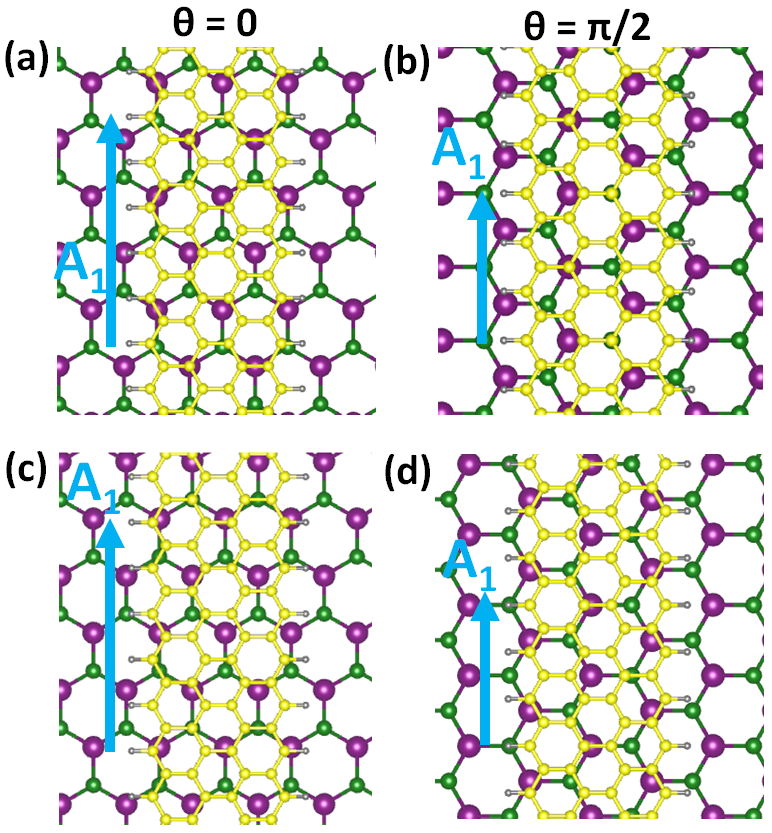
We consider heterostructures formed by AGNRs or ZGNRs placed on a monolayer TMD Mak et al. (2010); Ding et al. (2011); Xiao et al. (2012); Cappelluti et al. (2013); Shim et al. (2014); Reyes-Retana and Cervantes-Sodi (2016) as shown in Fig. 1 (a) where the ribbons are shown in yellow and the TMD monolayer in purple and green. To perform the ab-initio calculations the system must be periodic in all directions. For this reason an array of GNRs is placed on the TMD with periodic lattice constant . For the GNRs the direction is the longitudinal direction, and for the TMD substrate we denote by the axis formed by the intersection of the TMD plane with one of the mirror symmetry planes perpendicular to it. With these conventions we define the twist angle as the angle between the longitudinal, , axis of the GNR and the axis of the TMD monolayer.
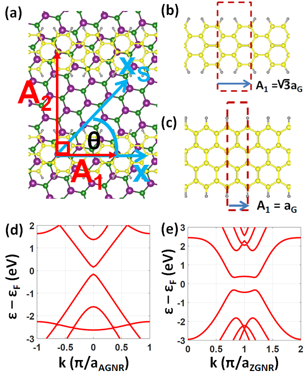
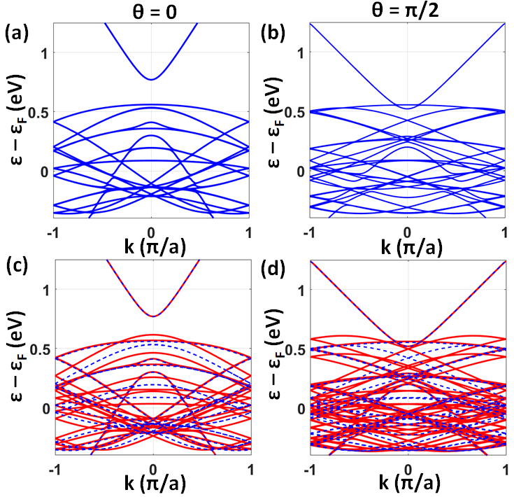
Graphene nanoribbons are of two types depending on the type of edges: armchair nanoribbons shown in Fig. 1 (b), and zigzag ribbons shown in Fig. 1 (c). The lattice constants for the two types of ribbons are =, =, for an AGNR and a ZGNR, respectively, with the graphene lattice constant. In all our calculations, to avoid the effect of dangling bonds, we terminate the edges of the GNRs with hydrogen atoms, shown as small grey spheres in Fig. 1. The band structure of both types of GNRs has a direct gap Nakada et al. (1996); Ezawa (2006); Barone et al. (2006); Fujita et al. (1996); Son et al. (2006); Yang et al. (2007); Dutta and Pati (2010); Palacios et al. (2010). In graphene the intrinsic spin-orbit coupling is extremely small, so much so that it has been suggested that graphene quantum dots based on AGNRs could be used to realize ideal spin-qubits Trauzettel et al. (2007). For this reason, to obtain the bands shown in Fig. 1, we have neglected corrections due to spin-orbit coupling. In ZGNRs the gap is close to and is due to electron-electron interactions that favor a ground state in which the electrons are ferromagnetically polarized along the edges and antiferromagnetically between the edges Lee et al. (2005); Son et al. (2006); Magda et al. (2014); Lee and Cho (2009); Yang et al. (2007); Jung et al. (2009); Ruffieux et al. (2016). AGNRs can be classified in three distinct groups depending on their chirality Nakada et al. (1996). Let be the width, in terms of carbon-carbon dimers aligned along the longitudinal direction. The three AGNRs’ chirality classes correspond to ribbons with width , , , . DFT results Son et al. (2006); Barone et al. (2006); Raza and Kan (2008) show that, contrary to the prediction of simple tight-binding models with constant hopping between the orbitals, all three types of AGNRs have a direct band gap at , and that this gap is much smaller for the class with . In the remainder we use for AGNRs and for ZGNRs.
TMD monolayers have an in-plane hexagonal structure as shown in Fig. 2 (a). Such a honeycomb lattice is best described as formed by two triangular sublattices: one sublattice is formed by the transition metal atoms, the darker and larger spheres in Fig. 2 (a), and the other by pairs of chalcogenide atoms, the lighter and smaller spheres in Fig. 2 (a). Fig. 2 (b) shows that the chalcogenide atoms are placed on two different planes, one below and one above the one formed by the transition metal atoms. We denote by the distance between the chalcogenide plane and the transition metal plane, and by the in-plane lattice constant. The lattice of the TMD substrate is characterized by two primitive vectors , and . For we use and , for we use and , values that are consistent with experimental values Bromley et al. (1972), and values obtained via ab-initio relaxation calculations Ding et al. (2011); Reyes-Retana and Cervantes-Sodi (2016)

All the electronic structures are obtained via ab-initio density functional theory (DFT) calculations using the Quantum Espresso package Giannozzi et al. (2017). We use a plane-waves basis with periodic boundary conditions. To perform the DFT calculation the one-dimensional GNR-TMD heterostructure is simulated as a three-dimensional periodic system in which an array of parallel GNRs is placed on the TMD with period , and each GNR-TMD layer is periodically replicated in the direction perpendicular to the plane with a vacuum interspace thick. The distance between ribbons, with the ribbon width, is chosen large enough to minimize interference effects between parallel ribbons. We find that the band structure of GNR-TMD heterostructures does not depend on for for the case when the ribbons are AGNRs and for the case when the ribbons are ZGNRs. We therefore set for AGNR-TMD systems and for ZGNR-TMD systems. We use the generalized gradient approximation (GGA) Perdew-Burke-Ernzerhof functional Perdew et al. (1996) to model the exchange-correlation term, and ultrasoft pseudopotential with a minimum kinetic energy cutoff for the charge density and the potential of 400 Ry. The minimum kinetic energy cutoff for planewave expansion was set to 50 Ry. The integration of the total energy was performed within the first Brillouin zone on the uniform k-points Monkhorst-Pack mesh Monkhorst and Pack (1976) with sizes for AGNR-, for AGNR-, for ZGNR-, and for ZGNR-. For each structure, the energy band structure was obtained with and without relativistic corrections to identify the effect of spin orbit coupling on the electronic structure of the GNR-TMD system.
To keep the presentation self-contained in the lower panels of Fig. 1 and Fig. 2 we show the band structure for the graphene nanoribbons and TMDs monolayers (when isolated) that form the GNR-TMD heterostructures that we study in the remainder. Figure 1 (d) shows the band structure obtained via ab-initio for an armchair graphene nanoribbon of width , and Fig. 1 (e) the band structure for a zigzag graphene nanoribbon of width , i.e., the ribbons’ width that we use in the remainder. Figure 2 (c) shows the band structure for and Fig. 2 (d) the one for . has a direct band gap equal to 1.33 eV whereas is metallic.
The key feature of TMDs monolayers is the presence of a strong spin-orbit-induced spin-splitting around the () points of the Brillouin Zone (BZ). The strength of the SOC can be quantified by the spin splitting at the K point of the conduction or valence band, whichever is largest. For the valence band has a spin splitting equal to 189 meV, for the the conduction band has the largest spin splitting, equal to 156 meV. Table 1 summarizes the key properties of the TMDs that we consider
| System | Gap(eV) | (meV) | (meV) | ||
|---|---|---|---|---|---|
| 3.33 | 1.674 | 1.33 | 189 | 21 | |
| 3.48 | 1.679 | - | - | 156 |
GNR-TMD heterostructures are characterized by a one dimensional primitive cell that depends on the stacking orientation of the GNR with respect to the TMD. To be able to obtain the bands of the heterostructure from first-principles we must restrict ourselves to commensurate stacking configurations. The condition for a commensurate stacking configuration can be expressed as:
| (1) |
where is the ribbon lattice constant, is the TMD lattice constant and are positive integers. Equation (1) implies that the integers must satisfy the equation:
| (2) |
For a triplet of integers that satisfies Eq. (2) the twist angle is obtained using Eq. (1) and for the heterostructure we have , see Fig. 1 (a).
Given the large size of the primitive cell of the GNR-TMD heterostructure it would be computationally very expensive to obtain the dependence of the system’s band structure on the twist angle.
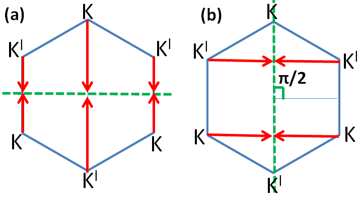
Considering that the intrinsic spin-orbit coupling of carbon atoms is extremely small, no matter how the inversion symmetry is broken (by lack of bulk inversion symmetry or by lack of surface inversion symmetry), the corresponding spin splitting of the bands is also very small. As a consequence the only significant SOC-induced spin splitting of the GNR bands in a GNR-TMD heterostructure has to come from the SOC-induced spin splitting of the TMD bands. The latter is due to bulk-inversion asymmetry. As a consequence for a quasi 1D GNR-TMD heterostructure in which the bulk inversion symmetry is restored, as in the case of Fig. 3 (a), one expects that the SOC-induced spin splitting of the bands will be much smaller than for a quasi 1D GNR-TMD heterostructure in which the bulk inversion asymmetry is preserved, as in the case of Fig. 3 (b). In general, for a GNR-TMD structure with bulk inversion symmetry the remaining, unavoidable, surface inversion asymmetry (SIA) can induce some amount of spin-splitting. We expect that this will be small compared to the one present when the GNR-TMD does not have bulk inversion symmetry. One of the goals of the calculations and results that we present in the remainder is to verify the accuracy of such expectation.
Based on the arguments above the (and the other values of related to by the point symmetry of the TMD lattice), and the (and the other values of related by symmetry) stacking configurations should be the ones that minimize, maximize, respectively, the spin-splitting in GNRs due to the proximity of the TMD monolayer. For this reason in the remainder we consider only these two stacking configurations. It should be pointed out, however, that fixing the twist angle does not fix completely the stacking configuration and therefore the symmetry properties of the structure: (i) one needs to further consider the folding of the bands along the direction of the GNR; (ii) by rigidly shifting the ribbon with respect to the substrate, or considering different amounts of strain for the ribbon or the substrate, different stacking configurations with the same twist angle can be realized. As a consequence, different stackings have different properties even if the twist angle is the same. However, as we discuss in the remainder, a lot can be understood about the general properties of GNR-TMD heterostructures by a careful analysis of the results obtained for specific and stacking configurations.
For the typical processes used to fabricate van der Waals heterostructures –in particular the widely used mechanical exfoliation process– the stacking configuration and the distance between the layers are not the ones corresponding to thermodynamic equilibrium, but the ones corresponding to some metastable configuration fixed by the details of the fabrication process and experimental conditions. As a consequence, confidence about the correct value of the distance between the layers forming a van der Waals system can only be achieved in the presence of experiments. Given that: (i) there are no experimental realizations yet of GNR-TMD heterostructures; (ii) it is expected that the value of the distance between GNR and TMD will be strongly dependent on the fabrication process; (iii) one of our main goals is to understand how the twist angle affects the SOC induced in the GNR by the TMD and to allow such a distance to depend on would prevent us to understand if and how the twist angle alone affects the key electronic properties of GNR-TMD heterostructures; (iv) The distance between GNR and TMD can be easily varied in experiments, for instance, by applying pressure; we adopt the following pragmatic approach. We perform a full relaxation calculation including van der Waals corrections for graphene- and graphene- heterostructures and obtain the values of the distance between graphene and TMD for these systems. We obtained and for graphene- and graphene-, respectively. We verified that these values are consistent with experimental measurements Ugeda et al. (2014); Kim et al. (2017) and previous ab-initio results Ma et al. (2011); Gmitra et al. (2016). We then used these values for the GNR-TMD heterostructures that we considered: for GNR- systems, for GNR- systems.
The reasons that led us to set the distance between GNR and TMD as described above, are some of the reasons why we did not do a full relaxation calculation to set the stacking between GNR and TMD. In addition to those reasons, we have that the primitive cells necessary to model GNR-TMD systems are very large and so: (i) it is computationally very expensive to do full relaxation calculations for all the structures that we need to consider to begin understand the effect of the twist angle on the electronic structure; (ii) in order to keep the number of atoms of the primitive cells below the limit above which the computational costs become prohibitive, we need to allow for some strain of the GNR’s lattice, and so the work to do a full relaxation calculations would be in vain. To be able to carry out the calculations we allowed for up to 6% uniform strain of the GNR’s lattice. Table. 2 shows the parameters for all the structures considered in the remainder of this work.
| System | Structure | Strain | |||
|---|---|---|---|---|---|
| GNR | |||||
| AGNR- | (4,3,3) | 3.33 | 1.5 | 17.3 | |
| AGNR- | (3,-4,4) | 3.33 | 4.2 | 13.3 | |
| AGNR- | (3,2,2) | 3.48 | -5.7 | 12.1 | |
| AGNR- | (4,-5,5) | 3.48 | 2.1 | 17.4 | |
| ZGNR- | (7,-3,-3) | 3.33 | 0.5 | 17.3 | |
| ZGNR- | (4,-3,3) | 3.33 | 1.5 | 9.99 | |
| ZGNR- | (5,-2,-2) | 3.48 | -2 | 12.05 | |
| ZGNR- | (3,-2,2) | 3.48 | -5.7 | 6.96 |
III Results: graphene nanoribbons on semiconducting TMD
III.1 AGNRs on semiconducting TMDs
In this section we present the results for the case of AGNRs on . Figure 4 (a), (b) show the stacking configuration for the case when , , respectively. These stackings correspond to the parameters shown on the first and second row of table 2, respectively.
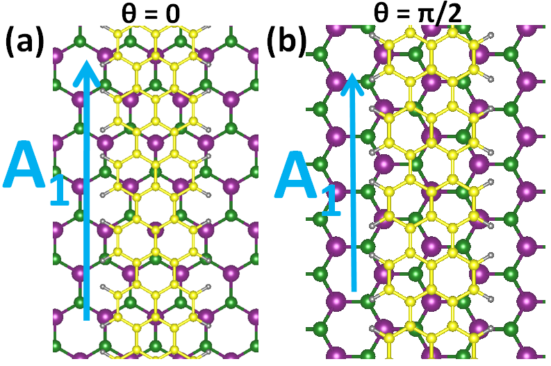
Figure 5 (a), (b) show the band structure of the AGNR- systems for the stacking configurations shown in 4 (a) and 4 (b), respectively. Due to the large band gap of the effect of the TMD proximity on the ribbon’s bands are small, and we can clearly identify the two lowest energy bands as the bands for which the electrons are mostly localized in the AGNR. For the configuration the band gap of the AGNR- heterostructure is 4.13% smaller than the band gap, 322 meV, of an isolated AGNR with the same uniform strain (1.5%) as the one used to obtain the commensurate stacking considered. For the the band gap is 4.92% smaller than the gap, 283 meV, of an isolated AGNR. These are relatively small changes that do not affect qualitatively the electronic properties of the ribbon. An enlargement of the low energy part of the bands, however, reveals that the AGNR’s valence band, due to the proximity of , exhibits a SOC-induced spin-splitting of the order of 1 meV, both for the case when and for the case when , as shown in Fig. 5 (c), (d). The spin-splitting is much smaller for the conduction bands, as shown by the blue lines in Fig. 5 (c), (d). This can be understood considering that for the isolated monolayer the SOC is much larger for the valence band states than for the conduction band states.
The spin-splitting induced by a semiconducting TMD monolayer on the low energy bands of an AGNR is not very large, but, being of the order on 1 meV, indicates that the SOC induced by proximity into the ribbon can be significant enough to allow the realization of topological superconducting states if the GNR-TMD structure is paired with a superconductor. The results of Fig. 5 show that to achieve this goal it would be advantageous to hole-dope the ribbon, given that the induced spin-orbit coupling is much larger for the ribbon’s valence band than for the conduction band.
III.2 ZGNRs on semiconducting TMDs
In Figure 6 (a), (b) the atomic structure of the stacking configurations corresponding to the 5th and 6th row of table 2 are shown. The configuration on the left panel corresponds to , whereas the one on the right panel corresponds to .
As mentioned in the introduction, in an isolated ZGNRs interactions lead to a ground state in which the spins are aligned ferromagnetically along the edges and antiferromagnetically between the edges. We denote this ground state as FA. Depending on the width of the ribbon the FA state can be very close in energy to a completely ferromagnetic state, the FF state, in which the spins on opposite edges are polarized in the same direction. For isolated ZGNRs that are as narrow as the ones that we consider in this work () the FA state is favored. The presence of a substrate Gani et al. (2018) can change the energy balance and favor the FF state or even a nonmagnetic state (NM) in which the spins at the edges are not polarized. For this reason, for all the TMD-ZGNR systems that we considered, we first checked which spin configuration (FA, FF, or NM) is favored.
The third column of table 3 shows the energy difference, per atom, between the NM state and the FA, and between the NM and the FF state, for an isolated ZGNR with and the same amount of strain used to realize the commensurate ZGNR- heterostructures shown in Fig. 6. We see that for the isolated ZGNR the FA state has always the lowest energy. The fifth column shows the energy difference between NM and FA state and NM and FF state for the ZGNR- heterostructures shown in Fig. 6. We see that the presence of the monolayer modifies the energy difference between FA and NM state, and between FF and NM state, but (for these configurations) not sufficiently to affect the energy ordering of the three possible spin configurations: the FA state is still the most favorable state. Given the results shown in table 3, in the remainder of this section we limit our discussion to the case when the ZGNR is in the FA spin configuration.
| Isolated ZGNR(N = 4) with strain | ZGNR- (N = 4) | |||
| State | (meV) | State | (meV) | |
| NM | 0 | NM | 0 | |
| FA | -7.4 | FA | -6.8 | |
| FF | -5.4 | FF | -5.3 | |
| NM | 0 | NM | 0 | |
| FA | -6.4 | FA | -5.9 | |
| FF | -4.4 | FF | -4.3 | |
Figure 7 shows the band structure of a ZGNR ribbon on for , left panels, and , right panels. In panels (a) and (b) the dashed lines show the result when the effects of SOC in are not taken into account, and the solid lines the bands obtained taking into account SOC. The two band structures appear to be qualitatively different, as it can be seen also from the dependence of the band gap on momentum shown in Fig. 7 (c), (d). On energy scales of the order of 100 meV, however, the apparent qualitative differences between the and the stacking are simply due to the different folding of the bands. Considering that for the structure with , and for the one with we have that in the first case the edge states of the ZGNR with momentum are folded to the momentum, whereas in the second case are folded to the point, .
To detect more physical differences we need to consider energy scales of the order of 1-10 meV. At these energy scales we observe that induces a -1.83% change of the band gap, compared to a band gap of 660 meV for isolated (strained) ZGNR, for the configuration, and a -2.11% gap change for the configuration for which the gap of an isolated ZGNR with the same amount of strain is 648 meV.

For the configuration the spin-splitting is completely negligible. On the contrary, for the configuration corresponding to the presence of induces a spin splitting of both the conduction and the valence band of ZGNR, see Fig. 8 (a), (b). In particular, Fig. 8 (a) shows that a spin-splitting is present even when SOC effects are neglected, and that such splitting is comparable to the one obtained when SOC are taken into account, Fig. 8 (b). The difference in spin splitting between the and configurations is due on the fact that for the stacking does not break (to very good approximation) the sublattice symmetry of the ribbon symmetry, whereas for significantly breaks such symmetry. Because at the edges of ZGNRs spin and sublattice symmetry are locked, the breaking of the sublattice symmetry due to the presence of the substrate induces a spin-splitting Soriano and Fernández-Rossier (2012). We encountered the same phenomenon when studying the electronic structure of ZGNRs on hexagonal boron nitride (hBN) Gani et al. (2018). The presence of SOC in has a only a small quantitative effect, as it can deduced by comparing Fig. 8 (b) to Fig. 8 (a).
For the stacking configuration considered the spin-splitting induced is not zero even for k=0, is even under parity, and of the order of 5 meV both when the TMD’s SOC is neglected or not. This shows that for this case the dominant contribution to the spin splitting is not due to SOC. The induced spin-splitting is akin to a Zeeman term: it breaks the Kramers degeneracy but it does not favor intraband s-wave pairing. These results suggest that, to use ZGNR- heterostructures to realize quasi 1D topological superconducting states, in addition to a component providing superconducting pairing, a source of SOC-induced spin polarization of the bands would be necessary.
IV Results: graphene nanoribbons on metallic TMD
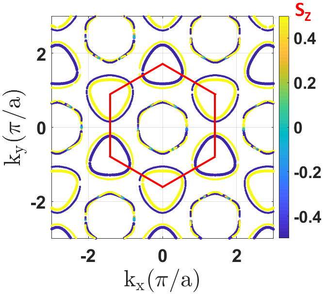
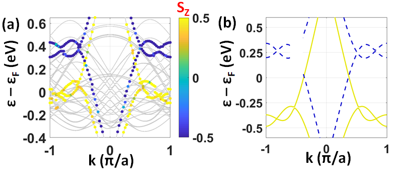
We now consider the case when the substrate is a monolayer of , that is metallic at room temperature. The Fermi surface (FS) of is characterized by pockets, around the point of the BZ and around the and points, as shown in Fig. 9.
IV.1 AGNRs on metallic TMDs
Figures 10 (a), (b) show the AGNR- heterostructures that we considered for the and case, respectively. The parameters defining these structures are given by the third and fourth row of Table 2.
Figures 11 (a), (b) show the bands for the and AGNR- structures shown in Fig. 10 (a), (b), respectively, when SOC effects are neglected. Panels (c), and (d), of Fig. 11 show the bands, as solid lines, when SOC is taken into account. To better show the effect of the SOC the bands obtained neglecting SOC are also shown as dashed lines.
Contrary to the case when the TMD is semiconducting, for the case when the TMD is metallic the low-energy band structures is much more intricate due to the coexistence of the folded bands of the substrate with the ones arising from the ribbon. To understand the effect of the metallic TMD substrate on the bands of the ribbon, for each momentum , we calculated the projection of the corresponding wave function onto the ribbon. The square of such projection, that we denote as , gives the probability that, for the state the electron is localized into the ribbon. By requiring we can identify which bands are “ribbon-like”, i.e., which bands have states that are mostly localized in the ribbon. After having done the projection of the states on the ribbon and identified which states are ribbon-like we can quantify confidently the effect of the metallic TMD substrate on the ribbon’s band structure. In particular we can extract: (i) amount of charge transfer; (ii) ribbon-substrate tunneling strength; (iii) presence of spin-splitting for ribbon-like bands.
Figures 12 (a), (b) show which low energy states have a probability equal or larger than 40% to be localized in the ribbon. From these figures we see that there is a charge transfer between and the AGNR that results in a p-doping of the ribbon. From Fig. 12 (a) we see that for the configuration the effective p-doping of the AGNR corresponds to a Fermy energy 0.3 eV below the top of the ribbon’s valence band. For the configuration, Fig. 12 (b), the charge transfer corresponds to a Fermy energy 0.21 eV below the top of ribbon’s valence band. The non negligible difference between the values of charge transfer is due to the fact that, to keep the number of atoms of the primitive cell below the limit above which calculations cannot be performed, for the two stacking configurations we had to set different amount of strain for the GNR, as shown in Table 2.
From Figs. 12 (a), (b) we can quantify the size of the gaps at the “avoided crossings” for the ribbon-like bands. For the configuration we observed gaps at avoided crossing as large as 55 meV, whereas for the case the largest avoided crossings are of the order of 30 meV. From these numbers we can estimate that for the AGNR- structure shown in Fig 10 (a) the effective interlayer tunneling, , at low energies, is of the order of 25 meV, and that AGNR- structure shown in Fig 10 (b) meV.
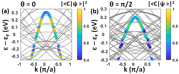
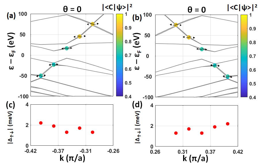
Figure 13 shows the bands –obtained including SOC– of the AGNR- heterostructure, in the stacking configuration, in a meV energy window around the Fermi energy for negative , panel (a), and positive , panel (b). The arrows denote the spin polarization. We see that for the states localized on the ribbon a spin-splitting is induced and that the spin polarizations for states with the same energy and opposite momentum are antiparallel. This shows that the induced spin-splitting is of the Rashba type. Figures 13 (c), (d) show the amplitude of the spin splitting as function of momentum. We see that the spin splitting is of the order of 2 meV, i.e. of the same order of magnitude as the one that we obtained for the case of AGNRs on semiconducting TMDs.
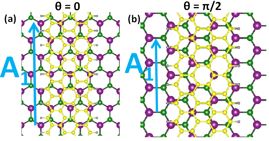
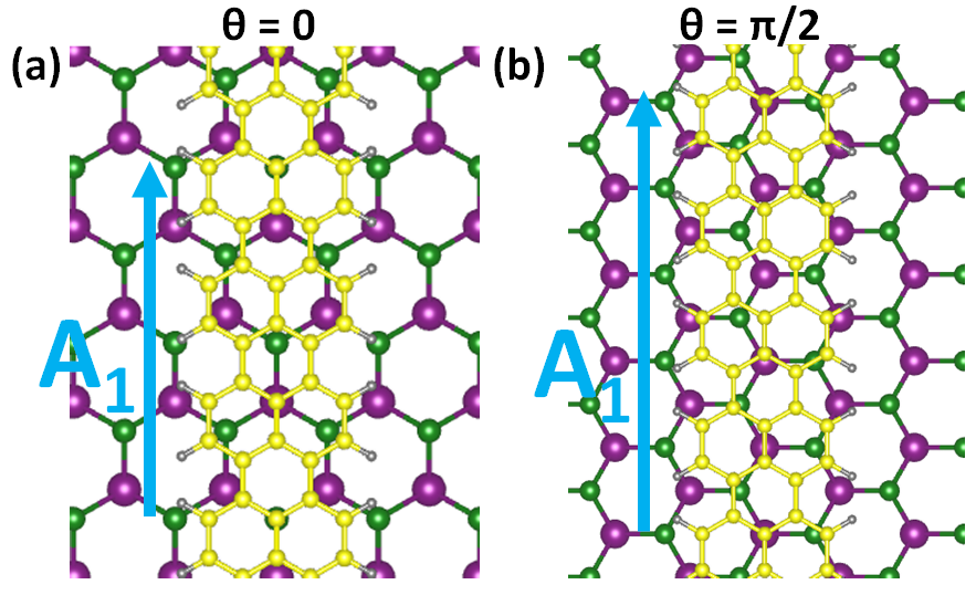
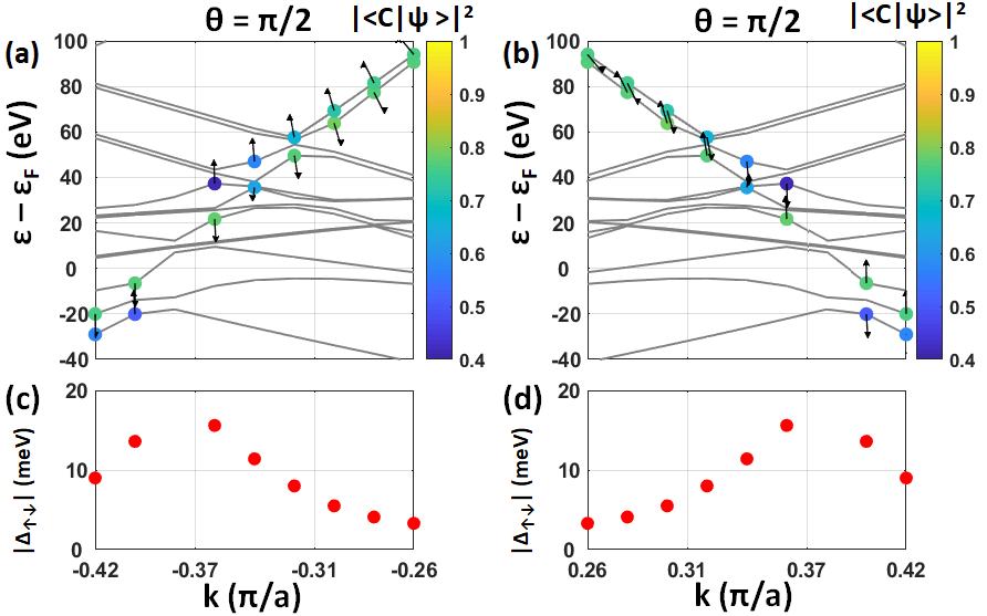
The magnitude of the spin-splitting induced into the AGNR by the proximity of is much larger for the stacking configuration, as shown in Fig. 14. Figures 14 (a), (b) show the spin-splitting of the low energy bands for which the projection of the wave function onto the ribbons is at least 40%, for positive and negative momenta, respectively. Figures 14 (c), (d) show the magnitude of the spin splitting as a function of momentum. We see that for the configuration the spin-splitting of the AGNR’s low-energy bands induced by can be as large as 15 meV, an order of magnitude larger than for the configuration. As discussed earlier, see Fig. 3, this is due to the fact that for the configuration the and valleys of the TMD, contrary to the case, do not fold into the same point of the reduced BZ reducing the cancellation of their opposite spin-splittings.
The large enhancement of the SOC of the AGNR, and the corresponding large spin-splitting of the low energy bands, induced by the proximity of the metallic TMD, make AGNR-TMD heterostructures with very interesting for the realization of quasi 1D topological superconducting states.
IV.2 ZGNRs on metallic TMDs
The case of ZGNRs on metallic TMDs monolayers is the most challenging case to consider. This is due to two reasons: (i) the fact that in ZGNRs the Coulomb interaction qualitatively affect the nature of the ground state Son et al. (2006); Yang et al. (2007); Fernández-Rossier (2008); (ii) the fact that the TMD, being metallic, can strongly modify, screen, the Coulomb interaction between electrons in the ZGNR and therefore modify the order, in terms of energy, of the possible ground states. As a consequence, for ZGNR-TMD heterostructures in which the TMD is metallic, the band structure of the ZGNR depend very strongly on the details of the stacking configuration.
To illustrate this fact in this section for each and configuration we consider also a “shifted” one having all the same parameters and differing only for a small rigid shift of the ribbon with respect to the TMD monolayer. The two stacking configurations are shown in Fig. 15 (a), (c). Given that the only difference between the two configurations is a shift of the ribbon, they both are characterized by the same and ribbon’s strain shown in the 7th row of table 2. Similarly the two stacking configurations are shown in Fig. 15 (b), (d), and their parameters in the 8th row of table 2. In the remainder we refer to the structures in the bottom panels of Fig. 15 as the “shifted” ones.
We then calculate the energy, per carbon atom, of the FF and FA state relative to the NM for each of the stacking configurations shown in Fig. 15. The results are shown in table 4. We see that for the “unshifted” stacking configurations, both for and , the FF state is energetically more favorable than the FA state, contrary to the case of isolated ZGNRs.
| ZGNR(N = 4) | ZGNR- (N = 4) | ||||
| State | (meV) | Shift | State | (meV) | |
| NM | 0 | N | NM | ||
| FA | -7.0 | N | FA | -1.32 | |
| FF | -5.0 | N | FF | -1.96 | |
| NM | 0 | Y | NM | -0.005 | |
| FA | -7.0 | Y | FA | -0.005-1.929 | |
| FF | -5.0 | Y | FF | -0.005-1.926 | |
| NM | 0 | N | NM | ||
| FA | -6.4 | N | FA | -1.62 | |
| FF | -4.8 | N | FF | -1.74 | |
| NM | 0 | Y | NM | -1.56 | |
| FA | -6.4 | Y | FA | -1.56-1.72 | |
| FF | -4.8 | Y | FF | -1.56-1.71 | |
Figure 16 (a) shows the band structure for the unshifted ZGNR- stacking configuration shown in Fig. 15 (b). The yellow and blue dots denotes the states for which the projection into the ribbon is larger than 50%, yellow and blue denoting opposite spin polarizations. For comparison, Fig. 16 (b) shows the bands of an isolated ZGNR in the FF state and with the same strain as the one used to realize the configuration whose bands are shown in panel (a). The results of Fig. 16 show that when the FF state is favored the ZGNR’s bands exhibit a very large spin-splitting, of the order of 0.5 eV at the edges of the 1D BZ, due to the ferromagnetic ordering. Such a large splitting, just marginally reduced, is still present in the unshifted ZGNR- structure due to the fact that the ribbon is in the FF state. In general, when the ZGNR is the FF state, the ferromagnetic ordering induces a very large spin-splitting and effects arising from the SOC in the substrate become negligible. For this reason, for ZGNR-TMD heterostructures for which the FF state is favored we have the qualitative result that the spin splitting of the ZGNR’s bands is of the order of few hundreds of meV, and to good approximation, independent of momentum, irrespective of the detail of the stacking configuration. For this reason, for ZGNR-TMD systems for which the FF state is the ribbon’s ground state no further analysis is required to know qualitatively the ZGNR’s band structure.
In the remainder, we focus on the and “shifted” structures, shown in Fig. 15 (c), (d), for which the FA state is the ribbon’s ground state. Figures 17 (a), (b) show the bands for the and structures, respectively, when SOC effects are neglected. Panels (c) and (d) of the same figure show the results with SOC. In these figures, to better emphasize the effect of SOC, the bands without SOC are also shown as dashed lines.
Figure 18 shows the low-energy bands for which the projection on the ribbon of the corresponding eigenstates is larger than 40%. Panels (a)-(d) show the results with no SOC, whereas (e)-(h) show the results with SOC. From these figures we see that, as for the case of AGNR- heterostructures, there is a charge transfer between the ZGNR and that makes the ribbon metallic and hole-doped, both for the and the structure. The hole doping correspond to a Fermi energy 30 meV (80 meV) below the top of the valence band for the () structure both with and without SOC.
Analysis of Figure 18 also allows us to identify the avoided crossings between ZGNR’s and TMD’s bands and, by measuring the gaps at this avoided crossings, estimate the strength of the tunneling between a ZGNR and TMD. For both the and configurations we observe gaps ranging between 2 and 10 meV, numbers that suggest a ZGNR-TMD tunneling strength of the order of just few meVs.


The projection of the bands on the ribbon allows us to identify the spin-splitting induced on the ribbon’s bands by the presence of the metallic TMD. Figure 19 show the results for the structure with no SOC. We see that the low energy ribbon’s bands are spin-splitted even when no SOC is present. As for the case of ZGNR on , this is a result of the fact that the substrate breaks the ribbon sublattice symmetry and therefore, given the nature of the FA state, the degeneracy between the spin polarized states localized at the opposite edges of the ribbon. The fact that the spin-splitting is due only to the breaking of the ribbon’s sublattice symmetry can also be inferred from the fact that states with opposite momentum have the same spin polarization. For the case, with no SOC, the maximum spin-splitting is of the order of 0.5 meV.
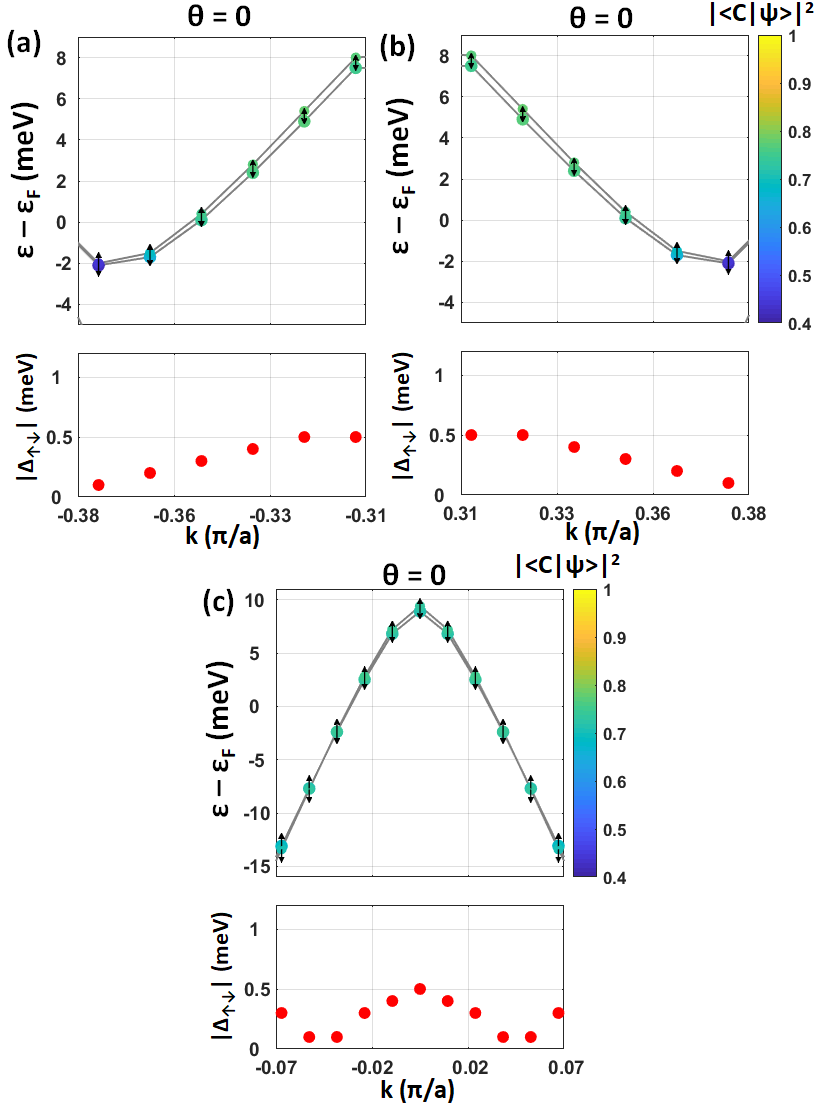
Figure 20 show the spin-splitting of the ribbon’s low energy bands for the structure with no SOC. As for the case, the breaking of the ribbon’s sublattice symmetry induces a spin-splitting of the bands. Again we notice that states with opposite momentum have the same spin polarization. However, for the particular structure considered, we have that the spin-splitting, even when SOC is neglected, is much larger than for the structure, meV, rather than meV. This can be assumed to be accidental and just due to differences between the two configurations for the relative alignment of the carbon atoms forming the ribbon and the substrate.

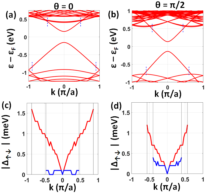
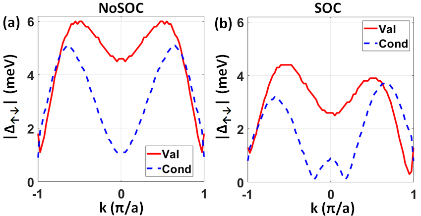
We now consider the case when SOC effects are included. Figure 21 show the results for the configuration obtained taking into account the presence of SOC. We see that the spin-splitting is of the order of 2 meV, larger than for the case when no SOC is included. However, we also notice that states with opposite momentum have approximately the same spin polarization. This suggests that the main mechanism by which a nonzero spin-splitting is induced into the ZGNR low energy bands is still the breaking of the sublattice symmetry combined with sublattice-spin lock for the edge state characteristic of the FA ground state.
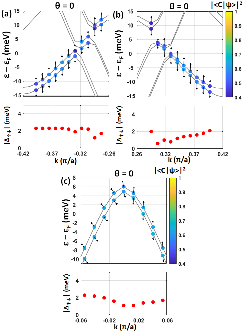
The situation is different for the stacking configuration. In this case the inclusion of SOC not only significantly enhances the spin-splitting of some of the bands, but it changes its nature given that now states with opposite momentum have opposite spin polarization, as shown in Fig. 22. In particular we see that for the conduction band the spin splitting when SOC is included is meV instead of meV when is SOC is not included.
By comparing the results of Fig. 21 with the ones of Fig. 22 we see that the SOC strongly affects the spin-splitting of the ZGNR’s bands when and only negligibly when . This can be understood from the general principle illustrated by Fig. 3: for stacking configurations the and valleys of the TMD do not fold on the same point of the reduced BZ and therefore the opposite spin splittings at these valleys of the TMD’s bands do not cancel as much as for the case of stacking configurations.

V Conclusions
In this work we have studied using first-principles the electronic structure of heterostructures formed by a graphene nanoribbon and a transition metal dichalcogenide monolayer. We have considered both armchair graphene nanoribbons and zigzag graphene nanoribbons on either a semiconducting or a metallic TMD monolayer. We have considered as the exemplary semiconducting TMD, and as the exemplary metallic one.
The presence of the ribbon causes the BZ of the monolayer to fold into a 1D BZ. Depending on the direction along which the ribbon is oriented with respect to the TMD we can have two extreme situations: either inequivalent or equivalent corners (valleys) of the TMD’s BZ fold to the same point on a line aligned along the 1D BZ of the GNR-TMD heterostructure. In the first case the spin-splitting induced into the ribbon will be minimized, in the second case it can be maximum. In our convention the first case correspond to stacking configurations with twist angle , and the second case to stacking configurations with . Rather than considering several stacking configurations we have focused on comparing the results for and configurations.
For the case when the TMD is a semiconductor we find that its effect on the ribbon’s band is quantitatively small. For armchair graphene nanoribbons the TMD causes a reduction of % of the band gap and a spin splitting of the order of 1 meV, for both the and the stacking configuration. The induced spin-splitting is small but it should be observable and possibly large enough to allow the formation of quasi 1D superconducting states in TMD-AGNR heterostructures that incorporate a superconducting layer. For zigzag graphene nanoribbons the induced spin-splitting is larger, of the order of 5 meV, for both the and the stacking configuration. In ZGNRs the electron-electron interactions favor the formation of ground states in which the spin are polarized. In isolated ZGNRs the state with the lowest energy is the FA state in which the spin are aligned ferromagnetically along the edges and antiferromagnetically between edges. Given that the atoms at opposite edges belong to different sublattices in the FA state, at the edges, the sublattice and the spin degrees of freedom are locked. A substrate, just by creating a different electrostatic potential for the two different edges, can break the sublattice symmetry and therefore, when the ZGNR is in the FA state, induce a spin-splitting even in the absence of SOC. This is the dominant mechanism by which the spin-splittings of meV that we obtain for ZGNR on are induced, for both the and the configuration.
For the case in which the TMD is metallic the effect of SOC is much more pronounced. In this case we notice a significant difference between and configurations. For AGNRs we find that for the configuration the induced spin-splitting is almost an order of magnitude larger than for the one. For we obtain a spin splitting of the order of 20 meV. For ZGNRs we find that the metallic TMD monolayer, depending on the details of the stacking configuration, can favor a ferromagnetic state for the ribbon rather than the FA state. For configurations for which the FA state remains the lowest energy state, we find that for stackings the induced spin-splitting can be as large as 40 meV, more than order of magnitude larger than for configurations.
One of the challenges in realizing Majorana modes in current quasi 1D superconductor-semiconductor heterostructures is the large number of subbands. As a consequence, to drive the system into a topological phase supporting Majorana modes requires very fine tuning of external gate voltages Antipov et al. (2018). A graphene nanoribbon is only one-atom thick and can be just few atoms wide. As a consequence in GNRs the bands are well separated in energy and to be in a situation in which only one band is at the Fermi energy does not require fine tuning. However, isolated GNRs have negligible spin-orbit coupling, one of the necessary ingredients to realize topological superconducting state. The results that we present show that a significant spin-orbit coupling can be induced in GNRs by proximitizing them to TMD monolayers, and that the resulting spin-splitting of the ribbon’s bands can be made quite large by stacking the ribbons in configurations that preserve bulk inversion asymmetry, i.e., minimize the folding of the opposite valley of the TMD’s bands to the same point of the 1D BZ. These results suggest that GNR-TMD heterostructures might be a promising new platform to realize topological superconducting states supporting Majorana modes as long as the quasi 1D GNR-TMD system can be engineered to have, in the normal phase, an odd number of bands crossing the Fermi energy by tuning the doping, and the strength of external magnetic field.
VI Acknowledgments
This work was supported by National Science Foundation Grant No. DMR-1455233 CAREER, Office of Naval Research Grant No. ONR-N00014-16-1-3158, and Army Research Office Grant No. W911NF-18-1-0290. E.R. acknowledges the Aspen Center for Physics, supported by National Science Foundation Grant No. PHY-1607611, and KITP, supported by the National Science Foundation under Grant No. NSF PHY-1748958, where part of this work was performed. The authors acknowledge William & Mary Research Computing for providing computational resources and technical support that have contributed to the results reported within this paper.
References
- Duerloo et al. (2014) Karel-Alexander N. Duerloo, Yao Li, and Evan J. Reed, “Structural phase transitions in two-dimensional mo- and w-dichalcogenide monolayers,” Nature Communications 5, 4214 (2014).
- Qian et al. (2014) Xiaofeng Qian, Junwei Liu, Liang Fu, and Ju Li, “Quantum spin hall effect in two-dimensional transition metal dichalcogenides,” Science 346, 1344–1347 (2014).
- Reyes-Retana and Cervantes-Sodi (2016) J. A. Reyes-Retana and F. Cervantes-Sodi, “Spin-orbital effects in metal-dichalcogenide semiconducting monolayers,” Scientific Reports 6, 24093 (2016).
- Xu et al. (2014) Xiaodong Xu, Wang Yao, Di Xiao, and Tony F. Heinz, “Spin and pseudospins in layered transition metal dichalcogenides,” Nature Physics 10, 343–350 (2014).
- Sie et al. (2019) Edbert J. Sie, Clara M. Nyby, C. D. Pemmaraju, Su Ji Park, Xiaozhe Shen, Jie Yang, Matthias C. Hoffmann, B. K. Ofori-Okai, Renkai Li, and Alexander H. et al. Reid, “An ultrafast symmetry switch in a weyl semimetal,” Nature 565, 61–66 (2019).
- Fatemi et al. (2018) Valla Fatemi, Sanfeng Wu, Yuan Cao, Landry Bretheau, Quinn D. Gibson, Kenji Watanabe, Takashi Taniguchi, Robert J. Cava, and Pablo Jarillo-Herrero, “Electrically tunable low-density superconductivity in a monolayer topological insulator,” Science 362, 926–929 (2018).
- Dvir et al. (2018) T. Dvir, F. Massee, L. Attias, M. Khodas, M. Aprili, C. H. L. Quay, and H. Steinberg, “Spectroscopy of bulk and few-layer superconducting nbse2 with van der waals tunnel junctions,” Nature Communications 9, 598 (2018).
- Pradhan et al. (2017) N. R. Pradhan, S. Talapatra, M. Terrones, P. M. Ajayan, and L. Balicas, “Optoelectronic properties of heterostructures: The most recent developments based on graphene and transition-metal dichalcogenides,” IEEE Nanotechnology Magazine 11, 18–32 (2017).
- Novoselov et al. (2004) K. S. Novoselov, A. K. Geim, S. V. Morozov, D. Jiang, Y. Zhang, S. V. Dubonos, I. V. Grigorieva, and A. A. Firsov, “Electric field effect in atomically thin carbon films,” Science 306, 666–669 (2004).
- An et al. (2018) Sung-Jin An, Yong Hwan Kim, Chanwoo Lee, Dae Young Park, and Mun Seok Jeong, “Exfoliation of transition metal dichalcogenides by a high-power femtosecond laser,” Scientific Reports 8, 12957 (2018).
- Li et al. (2014) Yilei Li, Alexey Chernikov, Xian Zhang, Albert Rigosi, Heather M. Hill, Arend M. van der Zande, Daniel A. Chenet, En-Min Shih, James Hone, and Tony F. Heinz, “Measurement of the optical dielectric function of monolayer transition-metal dichalcogenides: , , , and ,” Phys. Rev. B 90, 205422 (2014).
- (12) Seita Onishi, Miguel M. Ugeda, Yi Zhang, Yi Chen, Claudia Ojeda-Aristizabal, Hyejin Ryu, Sung-Kwan Mo, Zahid Hussain, Zhi-Xun Shen, Michael F. Crommie, and Alex Zettl, “Selenium capped monolayer nbse2 for two-dimensional superconductivity studies,” physica status solidi (b) 253, 2396–2399.
- Xi et al. (2015) Xiaoxiang Xi, Zefang Wang, Weiwei Zhao, Ju-Hyun Park, Kam Tuen Law, Helmuth Berger, László Forró, Jie Shan, and Kin Fai Mak, “Ising pairing in superconducting nbse 2 atomic layers,” Nature Physics 12, 139–143 (2015).
- Yang et al. (2018) Yafang Yang, Shiang Fang, Valla Fatemi, Jonathan Ruhman, Efrén Navarro-Moratalla, Kenji Watanabe, Takashi Taniguchi, Efthimios Kaxiras, and Pablo Jarillo-Herrero, “Enhanced superconductivity upon weakening of charge density wave transport in in the two-dimensional limit,” Phys. Rev. B 98, 035203 (2018).
- Navarro-Moratalla and Jarillo-Herrero (2016) Efren Navarro-Moratalla and Pablo Jarillo-Herrero, “The ising on the monolayer,” Nature Physics 12, 112 EP – (2016).
- Gmitra et al. (2009) M. Gmitra, S. Konschuh, C. Ertler, C. Ambrosch-Draxl, and J. Fabian, “Band-structure topologies of graphene: Spin-orbit coupling effects from first principles,” Phys. Rev. B 80, 235431 (2009).
- Wang et al. (2015) Z. Wang, DongKeun Ki, H. Chen, H Berger, A. H. MacDonald, and A. F. Morpurgo, “Strong interface-induced spin-orbit interaction in graphene on ws2,” Nature Comm. 6, 8339 (2015).
- Gmitra and Fabian (2015) Martin Gmitra and Jaroslav Fabian, “Graphene on transition-metal dichalcogenides: A platform for proximity spin-orbit physics and optospintronics,” Physical Review B 92, 155403 (2015).
- Gmitra et al. (2016) Martin Gmitra, Denis Kochan, Petra Högl, and Jaroslav Fabian, “Trivial and inverted dirac bands and the emergence of quantum spin hall states in graphene on transition-metal dichalcogenides,” Phys. Rev. B 93, 155104 (2016).
- Wang et al. (2016) Z. Wang, D. Ki, J. Y. Yong, Khoo, D. Mauro, H. Berger, Levitov L.S., and A. F. Morpurgo, “Origin and Magnitude of ’Designer’ Spin-Orbit Interaction in Graphene on Semiconducting Transition Metal dichalcogenides,” Phys. Rev. X 6, 041020 (2016).
- Yang et al. (2016) Bowen Yang, Min-Feng Tu, Jeongwoo Kim, Yong Wu, Hui Wang, Jason Alicea, Ruqian Wu, Marc Bockrath, and Jing Shi, “Tunable spin–orbit coupling and symmetry-protected edge states in graphene/WS2,” 2D Materials 3, 031012 (2016).
- Gmitra and Fabian (2017) Martin Gmitra and Jaroslav Fabian, “Proximity Effects in Bilayer Graphene on Monolayer WSe2: Field-Effect Spin Valley Locking, Spin-Orbit Valve, and Spin Transistor,” Physical Review Letters 119, 146401 (2017).
- Yang et al. (2017) Bowen Yang, Mark Lohmann, David Barroso, Ingrid Liao, Zhisheng Lin, Yawen Liu, Ludwig Bartels, Kenji Watanabe, Takashi Taniguchi, and Jing Shi, “Strong electron-hole symmetric rashba spin-orbit coupling in graphene/monolayer transition metal dichalcogenide heterostructures,” Phys. Rev. B 96, 041409 (2017).
- Völkl et al. (2017) Tobias Völkl, Tobias Rockinger, Martin Drienovsky, Kenji Watanabe, Takashi Taniguchi, Dieter Weiss, and Jonathan Eroms, “Magnetotransport in heterostructures of transition metal dichalcogenides and graphene,” Phys. Rev. B 96, 125405 (2017).
- Wakamura et al. (2018) T. Wakamura, F Reale, P. Palczynski, S. Gueron, C. Mattevi, and H Bouchiat, “Strong Anisotropic Spin-Orbit Interaction Induced in Graphene by Monolayer ws2,” Phys. Rev. Lett. 120, 106802 (2018).
- Zihlmann et al. (2018) Simon Zihlmann, Aron W. Cummings, Jose H. Garcia, Máté Kedves, Kenji Watanabe, Takashi Taniguchi, Christian Schönenberger, and Péter Makk, “Large spin relaxation anisotropy and valley-zeeman spin-orbit coupling in /graphene/-bn heterostructures,” Phys. Rev. B 97, 075434 (2018).
- Li and Koshino (2019) Yang Li and Mikito Koshino, “Twist-angle dependence of the proximity spin-orbit coupling in graphene on transition-metal dichalcogenides,” Physical Review B 99, 075438 (2019).
- David et al. (2019) Alessandro David, Péter Rakyta, Andor Kormányos, and Guido Burkard, “Induced spin-orbit coupling in twisted graphene–transition metal dichalcogenide heterobilayers: Twistronics meets spintronics,” Phys. Rev. B 100, 085412 (2019).
- Geim and Grigorieva (2013) A K Geim and I V Grigorieva, “Van der Waals heterostructures.” Nature 499, 419–25 (2013).
- Liu et al. (2016) Yuan Liu, Nathan O. Weiss, Xidong Duan, Hung-Chieh Cheng, Yu Huang, and Xiangfeng Duan, “Van der Waals heterostructures and devices,” Nature Reviews Materials 1, 16042 (2016).
- Novoselov et al. (2016) K S Novoselov, A Mishchenko, A Carvalho, and A H Castro Neto, “2D materials and van der Waals heterostructures,” Science 353, aac9439 (2016).
- Lu et al. (2016) Chih-Pin Lu, Martin Rodriguez-Vega, Guohong Li, Adina Luican-Mayer, Kenji Watanabe, Takashi Taniguchi, Enrico Rossi, and Eva Y. Andrei, “Local, global, and nonlinear screening in twisted double-layer graphene,” Proceedings of the National Academy of Sciences 113, 6623–6628 (2016).
- Rossi and Triola (2020) Enrico Rossi and Christopher Triola, “Van Der Waals Heterostructures with Spin‐Orbit Coupling,” Annalen der Physik 532, 1900344 (2020).
- Gani et al. (2019) Yohanes S. Gani, Hadar Steinberg, and Enrico Rossi, “Superconductivity in twisted graphene heterostructures,” Phys. Rev. B 99, 235404 (2019).
- Sau et al. (2010) Jay D. Sau, Roman M. Lutchyn, Sumanta Tewari, and S. Das Sarma, “Generic new platform for topological quantum computation using semiconductor heterostructures,” Phys. Rev. Lett. 104, 040502 (2010).
- Das et al. (2012) Anindya Das, Yuval Ronen, Yonatan Most, Yuval Oreg, Moty Heiblum, and Hadas Shtrikman, “Zero-bias peaks and splitting in an al-inas nanowire topological superconductor as a signature of majorana fermions,” Nature Physics 8, 887 (2012).
- Lutchyn et al. (2010) Roman M. Lutchyn, Jay D. Sau, and S. Das Sarma, “Majorana fermions and a topological phase transition in semiconductor-superconductor heterostructures,” Phys. Rev. Lett. 105, 077001 (2010).
- Alicea et al. (2011) Jason Alicea, Yuval Oreg, Gil Refael, Felix von Oppen, and Matthew P. A. Fisher, “Non-abelian statistics and topological quantum information processing in 1d wire networks,” Nature Physics 7, 412–417 (2011).
- Kitaev (2001) A Yu Kitaev, “Unpaired majorana fermions in quantum wires,” Physics-Uspekhi 44, 131 (2001).
- Nayak et al. (2008) Chetan Nayak, Steven H. Simon, Ady Stern, Michael Freedman, and Sankar Das Sarma, “Non-abelian anyons and topological quantum computation,” Rev. Mod. Phys. 80, 1083–1159 (2008).
- Cui et al. (2017) Ping Cui, Jin-Ho Choi, Wei Chen, Jiang Zeng, Chih-Kang Shih, Zhenyu Li, and Zhenyu Zhang, “Contrasting structural reconstructions, electronic properties, and magnetic orderings along different edges of zigzag transition metal dichalcogenide nanoribbons,” Nano Letters 17, 1097–1101 (2017).
- Gibertini and Marzari (2015) Marco Gibertini and Nicola Marzari, “Emergence of one-dimensional wires of free carriers in transition-metal-dichalcogenide nanostructures,” Nano Letters 15, 6229–6238 (2015), pMID: 26291826.
- Liu et al. (2013) Xiaofei Liu, Tao Xu, Xing Wu, Zhuhua Zhang, Jin Yu, Hao Qiu, Jin-Hua Hong, Chuan-Hong Jin, Ji-Xue Li, Xin-Ran Wang, Li-Tao Sun, and Wanlin Guo, “Top-down fabrication of sub-nanometre semiconducting nanoribbons derived from molybdenum disulfide sheets,” Nature Communications 4, 1776 EP – (2013), article.
- Klinovaja and Loss (2013) Jelena Klinovaja and Daniel Loss, “Spintronics in mos2 monolayer quantum wires,” Phys. Rev. B 88, 075404 (2013).
- Kumar and Ahluwalia (2014) Ashok Kumar and P.K. Ahluwalia, “Electronic transport and dielectric properties of low-dimensional structures of layered transition metal dichalcogenides,” Journal of Alloys and Compounds 587, 459 – 467 (2014).
- Chu et al. (2014) Rui-Lin Chu, Gui-Bin Liu, Wang Yao, Xiaodong Xu, Di Xiao, and Chuanwei Zhang, “Spin-orbit-coupled quantum wires and majorana fermions on zigzag edges of monolayer transition-metal dichalcogenides,” Phys. Rev. B 89, 155317 (2014).
- Chen et al. (2017) Yuxuan Chen, Ping Cui, Xibiao Ren, Chendong Zhang, Chuanhong Jin, Zhenyu Zhang, and Chih-Kang Shih, “Fabrication of mose2 nanoribbons via an unusual morphological phase transition,” Nature Communications 8, 15135 EP – (2017), article.
- Zan et al. (2018) Wenyan Zan, Zhuhua Zhang, Yang Yang, Xiaojun Yao, Sidian Li, and Boris I Yakobson, “Width-dependent phase crossover in transition metal dichalcogenide nanoribbons,” Nanotechnology 30, 075701 (2018).
- Dias et al. (2018) A. C. Dias, Fanyao Qu, David L. Azevedo, and Jiyong Fu, “Band structure of monolayer transition-metal dichalcogenides and topological properties of their nanoribbons: Next-nearest-neighbor hopping,” Phys. Rev. B 98, 075202 (2018).
- Chen et al. (2019) Tao Chen, Guolin Hao, Guang Wang, Bo Li, Liangzhi Kou, Hang Yang, Xiaoming Zheng, and Jianxin Zhong, “Controlled growth of atomically thin MoSe2 films and nanoribbons by chemical vapor deposition,” 2D Materials 6, 025002 (2019).
- Li et al. (2018) Shisheng Li, Yung-Chang Lin, Wen Zhao, Jing Wu, Zhuo Wang, Zehua Hu, Youde Shen, Dai-Ming Tang, Junyong Wang, Qi Zhang, Hai Zhu, Leiqiang Chu, Weijie Zhao, Chang Liu, Zhipei Sun, Takaaki Taniguchi, Minoru Osada, Wei Chen, Qing-Hua Xu, Andrew Thye Shen Wee, Kazu Suenaga, Feng Ding, and Goki Eda, “Vapour-liquid-solid growth of monolayer mos2 nanoribbons,” Nature Materials 17, 535–542 (2018).
- Zhang et al. (2014) Junhua Zhang, C. Triola, and E. Rossi, “Proximity effect in graphene-topological-insulator heterostructures,” Physical Review Letters 112, 096802 (2014).
- Triola et al. (2016) Christopher Triola, Driss M. Badiane, Alexander V. Balatsky, and E. Rossi, “General Conditions for Proximity-Induced Odd-Frequency Superconductivity in Two-Dimensional Electronic Systems,” Physical Review Letters 116, 257001 (2016).
- Rodriguez-Vega et al. (2017) M. Rodriguez-Vega, G. Schwiete, J. Sinova, and E. Rossi, “Giant edelstein effect in topological-insulator–graphene heterostructures,” Phys. Rev. B 96, 235419 (2017).
- Rodriguez-Vega et al. (2019) M. Rodriguez-Vega, G Schwiete, and Enrico Rossi, “Spin-charge coupled transport in van der Waals systems with random tunneling,” Physical Review Research 1, 033085 (2019).
- Jiao et al. (2010) Liying Jiao, Xinran Wang, Georgi Diankov, Hailiang Wang, and Hongjie Dai, “Facile synthesis of high-quality graphene nanoribbons,” Nature Nanotechnology 5, 321–325 (2010).
- Cai et al. (2010) Jinming Cai, Pascal Ruffieux, Rached Jaafar, Marco Bieri, Thomas Braun, Stephan Blankenburg, Matthias Muoth, Ari P. Seitsonen, Moussa Saleh, and Xinliang et al. Feng, “Atomically precise bottom-up fabrication of graphene nanoribbons,” Nature 466, 470–473 (2010).
- Ruffieux et al. (2016) Pascal Ruffieux, Shiyong Wang, Bo Yang, Carlos Sanchez-Sanchez, Jia Liu, Thomas Dienel, Leopold Talirz, Prashant Shinde, Carlo A. Pignedoli, Daniele Passerone, Tim Dumslaff, Xinliang Feng, Klaus Müllen, and Roman Fasel, “On-surface synthesis of graphene nanoribbons with zigzag edge topology,” Nature 531, 489 (2016).
- Narita et al. (2013) Akimitsu Narita, Xinliang Feng, Yenny Hernandez, Søren A. Jensen, Mischa Bonn, Huafeng Yang, Ivan A. Verzhbitskiy, Cinzia Casiraghi, Michael Ryan Hansen, and Amelie H. R. et al. Koch, “Synthesis of structurally well-defined and liquid-phase-processable graphene nanoribbons,” Nature Chemistry 6, 126–132 (2013).
- Rizzo et al. (2018) Daniel J. Rizzo, Gregory Veber, Ting Cao, Christopher Bronner, Ting Chen, Fangzhou Zhao, Henry Rodriguez, Steven G. Louie, Michael F. Crommie, and Felix R. Fischer, “Topological band engineering of graphene nanoribbons,” Nature 560, 204–208 (2018).
- Gröning et al. (2018) Oliver Gröning, Shiyong Wang, Xuelin Yao, Carlo A. Pignedoli, Gabriela Borin Barin, Colin Daniels, Andrew Cupo, Vincent Meunier, Xinliang Feng, Akimitsu Narita, Klaus Müllen, Pascal Ruffieux, and Roman Fasel, “Engineering of robust topological quantum phases in graphene nanoribbons,” Nature 560, 209–213 (2018).
- Mattheiss (1973) L. F. Mattheiss, “Band structures of transition-metal-dichalcogenide layer compounds,” Phys. Rev. B 8, 3719–3740 (1973).
- Terrones and Terrones (2014) Humberto Terrones and Mauricio Terrones, “Bilayers of transition metal dichalcogenides: Different stackings and heterostructures,” Journal of Materials Research 29, 373–382 (2014).
- Mak et al. (2010) Kin Fai Mak, Changgu Lee, James Hone, Jie Shan, and Tony F. Heinz, “Atomically thin : A new direct-gap semiconductor,” Phys. Rev. Lett. 105, 136805 (2010).
- Ding et al. (2011) Yi Ding, Yanli Wang, Jun Ni, Lin Shi, Siqi Shi, and Weihua Tang, “First principles study of structural, vibrational and electronic properties of graphene-like MX2 (M=Mo, Nb, W, Ta; X=S, Se, Te) monolayers,” Physica B: Condensed Matter 406, 2254 – 2260 (2011).
- Xiao et al. (2012) Di Xiao, Gui-Bin Liu, Wanxiang Feng, Xiaodong Xu, and Wang Yao, “Coupled spin and valley physics in monolayers of and other group-vi dichalcogenides,” Phys. Rev. Lett. 108, 196802 (2012).
- Cappelluti et al. (2013) E. Cappelluti, R. Roldán, J. A. Silva-Guillén, P. Ordejón, and F. Guinea, “Tight-binding model and direct-gap/indirect-gap transition in single-layer and multilayer mos2,” Phys. Rev. B 88, 075409 (2013).
- Shim et al. (2014) Gi Woong Shim, Kwonjae Yoo, Seung-Bum Seo, Jongwoo Shin, Dae Yool Jung, Il-Suk Kang, Chi Won Ahn, Byung Jin Cho, and Sung-Yool Choi, “Large-area single-layer mose2 and its van der waals heterostructures,” ACS Nano 8, 6655–6662 (2014).
- Nakada et al. (1996) Kyoko Nakada, Mitsutaka Fujita, Gene Dresselhaus, and Mildred S Dresselhaus, “Edge state in graphene ribbons: Nanometer size effect and edge shape dependence,” Physical Review B 54, 17954–17961 (1996).
- Ezawa (2006) Motohiko Ezawa, “Peculiar width dependence of the electronic properties of carbon nanoribbons,” Phys. Rev. B 73, 045432 (2006).
- Barone et al. (2006) Verónica Barone, Oded Hod, and Gustavo E. Scuseria, “Electronic structure and stability of semiconducting graphene nanoribbons,” Nano Letters 6, 2748–2754 (2006), pMID: 17163699.
- Fujita et al. (1996) Mitsutaka Fujita, Katsunori Wakabayashi, Kyoko Nakada, and Koichi Kusakabe, “Peculiar localized state at zigzag graphite edge,” Journal of the Physical Society of Japan 65, 1920–1923 (1996).
- Son et al. (2006) Young-Woo Son, Marvin L. Cohen, and Steven G. Louie, “Energy gaps in graphene nanoribbons,” Phys. Rev. Lett. 97, 216803 (2006).
- Yang et al. (2007) L Yang, C-H. Park, Y-W. Son, M L Cohen, and S G Louie, “Quasiparticle Energies and Band Gaps in Graphene Nanoribbons,” Phys. Rev. Lett. 99, 186801 (2007).
- Dutta and Pati (2010) Sudipta Dutta and Swapan K. Pati, “Novel properties of graphene nanoribbons: a review,” Journal of Materials Chemistry 20, 8207 (2010).
- Palacios et al. (2010) J J Palacios, J Fernández-Rossier, L Brey, and H A Fertig, “Electronic and magnetic structure of graphene nanoribbons,” Semiconductor Science and Technology 25, 033003 (2010).
- Trauzettel et al. (2007) Björn Trauzettel, Denis V. Bulaev, Daniel Loss, and Guido Burkard, “Spin qubits in graphene quantum dots,” Nature Physics 3, 192 (2007).
- Lee et al. (2005) Hosik Lee, Young-Woo Son, Noejung Park, Seungwu Han, and Jaejun Yu, “Magnetic ordering at the edges of graphitic fragments: Magnetic tail interactions between the edge-localized states,” Phys. Rev. B 72, 174431 (2005).
- Magda et al. (2014) Gábor Zsolt Magda, Xiaozhan Jin, Imre Hagymási, Péter Vancsó, Zoltán Osváth, Péter Nemes-Incze, Chanyong Hwang, László P. Biró, and Levente Tapasztó, “Room-temperature magnetic order on zigzag edges of narrow graphene nanoribbons,” Nature 514, 608–611 (2014).
- Lee and Cho (2009) Geunsik Lee and Kyeongjae Cho, “Electronic structures of zigzag graphene nanoribbons with edge hydrogenation and oxidation,” Phys. Rev. B 79, 165440 (2009).
- Jung et al. (2009) J. Jung, T. Pereg-Barnea, and A. H. MacDonald, “Theory of interedge superexchange in zigzag edge magnetism,” Phys. Rev. Lett. 102, 227205 (2009).
- Raza and Kan (2008) Hassan Raza and Edwin C Kan, “Armchair graphene nanoribbons: Electronic structure and electric-field modulation,” Physical Review B 77, 245434 (2008).
- Bromley et al. (1972) R A Bromley, R B Murray, and A D Yoffe, “The band structures of some transition metal dichalcogenides. III. Group VIA: trigonal prism materials,” Journal of Physics C: Solid State Physics 5, 759 (1972).
- Giannozzi et al. (2017) P Giannozzi, O Andreussi, T Brumme, O Bunau, M Buongiorno Nardelli, M Calandra, R Car, C Cavazzoni, D Ceresoli, M Cococcioni, N Colonna, I Carnimeo, A Dal Corso, S de Gironcoli, P Delugas, R A DiStasio Jr, A Ferretti, A Floris, G Fratesi, G Fugallo, R Gebauer, U Gerstmann, F Giustino, T Gorni, J Jia, M Kawamura, H-Y Ko, A Kokalj, E Küçükbenli, M Lazzeri, M Marsili, N Marzari, F Mauri, N L Nguyen, H-V Nguyen, A Otero de-la Roza, L Paulatto, S Poncé, D Rocca, R Sabatini, B Santra, M Schlipf, A P Seitsonen, A Smogunov, I Timrov, T Thonhauser, P Umari, N Vast, X Wu, and S Baroni, “Advanced capabilities for materials modelling with QUANTUM ESPRESSO,” Journal of Physics: Condensed Matter 29, 465901 (2017).
- Perdew et al. (1996) John P. Perdew, Kieron Burke, and Matthias Ernzerhof, “Generalized gradient approximation made simple,” Phys. Rev. Lett. 77, 3865–3868 (1996).
- Monkhorst and Pack (1976) Hendrik J. Monkhorst and James D. Pack, “Special points for brillouin-zone integrations,” Phys. Rev. B 13, 5188–5192 (1976).
- Ugeda et al. (2014) Miguel M. Ugeda, Aaron J. Bradley, Su Fei Shi, Felipe H. Da Jornada, Yi Zhang, Diana Y. Qiu, Wei Ruan, Sung Kwan Mo, Zahid Hussain, Zhi Xun Shen, Feng Wang, Steven G. Louie, and Michael F. Crommie, “Giant bandgap renormalization and excitonic effects in a monolayer transition metal dichalcogenide semiconductor,” Nature Materials 13, 1091–1095 (2014).
- Kim et al. (2017) Minsoo Kim, Geon Hyoung Park, Jongyun Lee, Jae Hyeong Lee, Jinho Park, Hyunwoo Lee, Gil Ho Lee, and Hu Jong Lee, “Strong Proximity Josephson Coupling in Vertically Stacked NbSe2-Graphene-NbSe2 van der Waals Junctions,” Nano Letters 17, 6125–6130 (2017).
- Ma et al. (2011) Yandong Ma, Ying Dai, Wei Wei, Chengwang Niu, Lin Yu, and Baibiao Huang, “First-principles study of the graphene@MoSe2 heterobilayers,” Journal of Physical Chemistry C 115, 20237–20241 (2011).
- Gani et al. (2018) Yohanes S. Gani, D. S. L. Abergel, and Enrico Rossi, “Electronic structure of graphene nanoribbons on hexagonal boron nitride,” Phys. Rev. B 98, 205415 (2018).
- Soriano and Fernández-Rossier (2012) D. Soriano and J. Fernández-Rossier, “Interplay between sublattice and spin symmetry breaking in graphene,” Physical Review B - Condensed Matter and Materials Physics 85, 195433 (2012).
- Fernández-Rossier (2008) J. Fernández-Rossier, “Prediction of hidden multiferroic order in graphene zigzag ribbons,” Phys. Rev. B 77, 075430 (2008).
- Antipov et al. (2018) Andrey E. Antipov, Arno Bargerbos, Georg W. Winkler, Bela Bauer, Enrico Rossi, and Roman M. Lutchyn, “Effects of gate-induced electric fields on semiconductor majorana nanowires,” Phys. Rev. X 8, 031041 (2018).