Critical role of device geometry for the phase diagram of twisted bilayer graphene
Abstract
The effective interaction between electrons in two-dimensional materials can be modified by their environment, enabling control of electronic correlations and phases. Here, we study the dependence of electronic correlations in twisted bilayer graphene (tBLG) on the separation to the metallic gate(s) in two device configurations. Using an atomistic tight-binding model, we determine the Hubbard parameters of the flat bands as a function of gate separation, taking into account the screening from the metallic gate(s), the dielectric spacer layers and the tBLG itself. We determine the critical gate separation at which the Hubbard parameters become smaller than the critical value required for a transition from a correlated insulator state to a (semi-)metallic phase. We show how this critical gate separation depends on twist angle, doping and the device configuration. These calculations may help rationalise the reported differences between recent measurements of tBLG’s phase diagram and suggests that correlated insulator states can be screened out in devices with thin dielectric layers.
I Introduction
Twisted bilayer graphene (tBLG) has emerged as a highly tunable platform (through twist angle, hydrostatic pressure, and doping) for studying the behaviour of correlated electrons in two dimensions Cao et al. (2018a, b); Yankowitz et al. (2019); Lu et al. (2019); Xie et al. (2019); Kerelsky et al. (2019); Jiang et al. (2019); Carr et al. (2018). Several groups have reported the experimental observation of correlated insulator states in both doped and undoped tBLG near the magic twist angle Cao et al. (2018a, b); Yankowitz et al. (2019); Lu et al. (2019). Despite much theoretical work, no consensus has yet been reached regarding the microscopic mechanism of these phases Liao et al. (2019); Yan et al. (2018); Kennes et al. (2018); Sherkunov and Betouras (2018); Kang and Vafek (2018a); González and Stauber (2019); Liu et al. (2018); Xie and MacDonald (2019); Padhi et al. (2018); Choi and Choi (2018); Po et al. (2018); Pizarro et al. (2019a); Wu et al. (2018); Ochi et al. (2018); Wu (2019); Roy and Juric̆ić (2019); Guinea and Walet (2018). Superconductivity is also found at low temperatures Cao et al. (2018b); Yankowitz et al. (2019); Lu et al. (2019), but neither the nature of the pairing interaction nor the symmetry of the superconducting order parameter have been determined.
Importantly, significant differences in the measured phase diagrams have been reported Cao et al. (2018a, b); Yankowitz et al. (2019); Lu et al. (2019): some groups have found correlated insulator states at doping levels where other groups find semi-metallic or metallic behaviour Cao et al. (2018a, b); Yankowitz et al. (2019); Lu et al. (2019). Also, different numbers of superconducting states as a function of doping have been reported Cao et al. (2018b); Yankowitz et al. (2019); Lu et al. (2019). It has been suggested that these differences are a consequence of the varying degree of twist-angle homogeneity in the tBLG samples Lu et al. (2019).
Another potential origin of the variations in the observed phase diagram are differences in the device setups employed in the experiments. For example, Cao et al. Cao et al. (2018a, b) used devices in which the tBLG is encapsulated by hexagonal boron-nitride (hBN) slabs of 10-30 nm thickness with gold gates on either side. In contrast, Yankowitz et al. Yankowitz et al. (2019) used thicker hBN slabs (30-60 nm) that are sandwiched between two graphite gates, and the device of Lu et al. Lu et al. (2019) only had a single graphite gate separated from the tBLG by a hBN layer of nm thickness.
The device setup is important because the dielectric environment in which tBLG is situated will have a strong influence on the screened interaction between the electrons in tBLG Pizarro et al. (2019b), which will in turn affect the phase diagram. For gated tBLG devices, the potential induced by an electron in the tBLG is reduced by the image charge in the metallic gate(s). The strength of the resulting effective interaction between electrons in the tBLG is determined by the separation of the metallic gate(s) from the tBLG which can be experimentally controlled via the thickness of a dielectric spacer layer (typically hBN).
In this article, we investigate the dependence of electron correlations in tBLG devices on the distance between tBLG and the metallic gate(s) (or equivalently, the thickness of the hBN layer). Starting from an atomistic tight-binding model, we construct Wannier functions of the flat bands and calculate the corresponding Hubbard parameters taking into account screening from the metallic gates, the hBN and the tBLG itself. We find that the Hubbard parameters depend sensitively on the gate distance enabling precise control of electron correlations via device geometry. We calculate the critical gate distances at which the correlated insulator states disappear and predict detailed phase diagrams as function of doping. We also discuss the interplay of device geometry and superconductivity and hypothesize that small gate separations should weaken correlated insulator states, but strengthen superconducting phases.
II Methods
To model the electronic structure of tBLG near the magic angle, we employ the techniques described in detail in Refs. 27 and 28. For convenience, we summarize briefly the method here. To obtain the electronic band structure of tBLG, we carry out atomistic tight-binding calculations using the parameters of Ref. 29. Next, Wannier functions (with denoting both the unit cell and the band-like index of the Wannier function) of the flat bands are generated Koshino et al. (2018); Marzari et al. (2012); Pizzi et al. (2019); Kang and Vafek (2018b); Goodwin et al. (2019a, b). The extended Hubbard parameters of the flat band electrons are obtained by evaluating
| (1) |
where denotes the screened interaction between electrons, which is determined by screening processes inside tBLG (internal screening), but also has contributions from the environment.
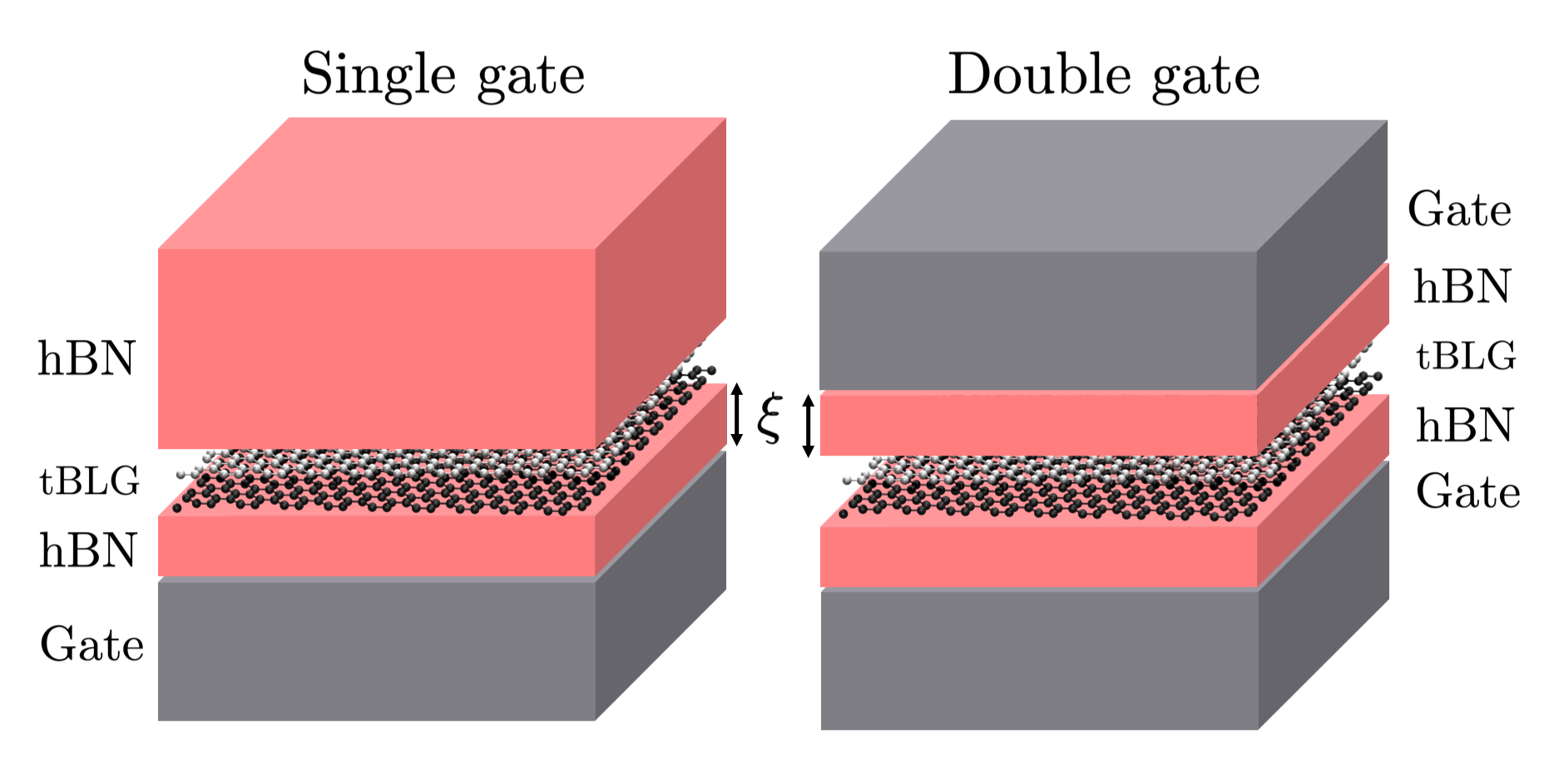
In a typical device configuration, the tBLG is encapsulated by a dielectric substrate [usually hexagonal boron nitride (hBN)] which separates it from the metallic gate(s). Here, we investigate two device types: (i) tBLG with a bottom gate only (i.e., gate/hBN/tBLG/hBN, where it is assumed that the hBN on top is very thick and can be approximated by a semi-infinite dielectric, while the hBN layer that separates the tBLG and the gate has a thickness , see left panel of Fig. 1); and (ii) tBLG with both a top and a bottom gate (i.e., gate/hBN/tBLG/hBN/gate, where both hBN layers have the same thickness , see right panel of Fig. 1). The gates are modelled as semi-infinite ideal metals.
For the single-gate device, the electrostatic image charge interaction results in a screened interaction of the form
| (2) |
where is the electron charge, is the permittivity of free space, and denotes the dielectric constant due to screening from the tBLG and the hBN. We have assumed that the tBLG lies in the -plane ( denotes the unit vector pointing in the -direction) and that corresponds to the thickness of hBN (distance from the metallic gate to the bottom of the tBLG). In principle, the internal screening from the tBLG leads to a complicated wave-vector dependent dielectric function, but Goodwin et al. Goodwin et al. (2019b) have previously shown that—near the magic angle—the Hubbard parameters within the constrained random phase approximation (cRPA) can be accurately reproduced using a bare Coulomb interaction divided by the cRPA dielectric constant of a decoupled bilayer graphene (8.86) Goodwin et al. (2019b). To describe the screening by the dielectric substrate we add to this the bulk dielectric constant of hBN (3.9) Xue et al. (2011) and subtract one to avoid double-counting the dielectric constant of free space resulting in . For the double-gate device, the screened interaction is given by Throckmorton and Vafek (2012)
| (3) |
For in-plane distances much smaller than , this screened interaction reduces to the bare Coulomb interaction divided by . For in-plane distances much larger than , the screened interaction can be expressed as Throckmorton and Vafek (2012). Here we assume that in the image-potential the tBLG resides in the plane, which again means corresponds to the thickness of the hBN spacer.
III Results and Discussion
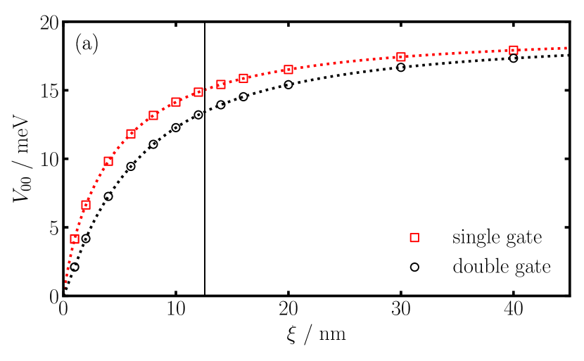
Figure 2(a) shows the on-site Hubbard parameter of tBLG as a function of the gate separation for a twist angle of 1.12, for both single-gate and double-gate device configurations (other twist angles are shown in Appendix A). The largest values of are obtained for large gate separations, and there is a substantial reduction in as the gate separation decreases below the moiré length (indicated by the vertical line in Fig. 2). This can be understood from Eqs. (2) and (3) where the image charge contribution arising from the induced charge density at the surface of the gate reduces the Coulomb interaction between electrons in the tBLG. In the case of the single-gate device, when is small, the electron in the tBLG and its image charge effectively interact with other electrons via a weak dipolar potential (instead of the usual monopole charge-charge interaction). For the double-gate setup, the image charges in both gates give rise to an exponentially screened interaction between electrons in the tBLG. The results for in the two different device configurations are qualitatively similar, but the Hubbard parameters are somewhat smaller for the double-gate setup since both of the gates contribute to the screening.
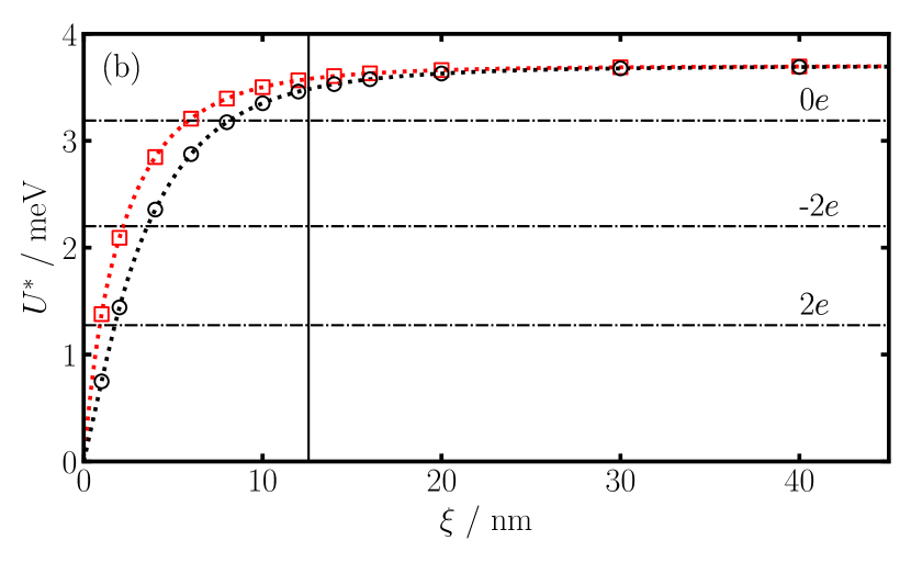
In the Hubbard model Hubbard (1963, 1964), electron-electron interactions are assumed to be short-ranged and the strength of electron correlations is usually measured by the ratio of the on-site Hubbard parameter and the nearest-neighbor hopping parameter . A system with long-ranged electron-electron interactions can be mapped onto an effective Hubbard model with an on-site Hubbard parameter (reflecting the energy required to hop from an empty Wannier orbital to an occupied neighbor site), where is the interaction between Wannier functions centred on neighbouring AB/BA regions (see Fig. A1 of Appendix A for as a function of ) Schüler et al. (2013); Goodwin et al. (2019a, b). Fig. 2(b) shows for tBLG as function of for a twist angle of 1.12 for both device configurations (results for other twist angles are shown in Appendix A). It can be seen that is significantly smaller than , indicating that interactions between neighboring Wannier functions play an important role even in the presence of metallic gates Goodwin et al. (2019a, b). This is expected as there is significant overlap between lobes of neighboring Wannier functions Koshino et al. (2018); Goodwin et al. (2019a). Similarly to , approaches a constant value in the limit of distant gates, but does so more rapidly once becomes larger than the moiré length. Moreover, exhibits a significantly sharper reduction as the distance decreases. Naively, one might expect that the presence of gates should lead to an increase in if the screened interaction is sufficiently short-ranged such that is strongly reduced. We find indeed that decreases more quickly than (see Appendix A), but this relative reduction of compared to is not sufficient to overcome the large absolute reduction of [see Fig. 2(a)] and, therefore, the overall balance is such that decreases with decreasing .
III.1 Correlated Insulators
When reaches a critical value, a phase transition from a (semi-)metallic phase to a correlated insulator state is expected. For tBLG, no consensus has yet been reached regarding the nature of the correlated insulator states, nor the corresponding value of the critical . For Bernal stacked bilayer graphene, Quantum Monte Carlo calculations have found a critical value of for a phase transition to a gapped antiferromagnetic phase Lang et al. (2012). Recently, Klebl and Honerkamp calculated the phase diagram of tBLG using an atomistic RPA approach Klebl and Honerkamp (2019). For undoped tBLG (denoted ), they find a transition from a semi-metal to an antiferromagnetic insulator, and for doping levels corresponding to two extra electrons () or holes () per moiré cell, a transition from a metallic phase to a ferromagnetic insulator is predicted. The RPA value for the critical in tBLG is smaller than in the Bernal stacked bilayer, and depends both on temperature and doping. Because of the lack of self-energy corrections, the critical values from the RPA should be considered as lower bounds Klebl and Honerkamp (2019).

In Fig. 2(b), the critical values of for the cases of , and doping are indicated by horizontal dotted-dashed lines. Here, we have multiplied the critical (where is the hopping parameter of graphene) values from Klebl and Honerkamp Klebl and Honerkamp (2019) at a temperature K with the hopping parameter between neighbouring Wannier functions (calculated from the width of the flat bands in our atomistic tight-binding model using , which is the relation between bandwidth and hopping in graphene). For the single-gate (double-gate) device, as the gate separation is reduced to nm ( nm), crosses the critical value for zero doping, indicating that tBLG would exhibit a semi-metallic phase at zero doping, but correlated insulator states at and doping. At nm ( nm), the critical for doping is crossed and finally, at nm ( nm) the critical value for doping is reached. For even smaller values of , the tBLG is either metallic or semi-metallic at the doping levels considered here. These results demonstrate that the phase diagram of tBLG can be controlled via the thickness of the dielectric substrate that separates the tBLG from the metallic gates and, hence, determines the degree to which the gate is able to screen electron-electron interactions in tBLG. The critical separations for phase transitions depend on the device configuration, with smaller values for single-gate devices because the screening is weaker than in double-gate devices.
The critical gate separation also depends on the twist angle. Fig. 3 shows this dependence as a function of twist angle from the magic angle for the single-gate device configuration and for three doping levels: (left panel), (middle panel) and (right panel) at K. The equivalent result for the double-gate configuration is shown in Appendix B. For all doping levels, decreases as the magic angle is approached. Close to the magic angle, the hopping approaches zero and extremely small values of must be achieved to reach the critical value of . This is only possible for very small values of . Comparing the three doping levels, we find that for the undoped system increases most rapidly away from the magic angle. At twist angles larger than from the magic angle, the undoped system is always metallic and no phase transition to a correlated insulator phase can be induced. For doping, the critical twist angle window is larger than for zero doping. For doping, a critical thickness can be found for all considered twist angles near the magic angle. At larger temperatures, the critical value of is smallest at charge neutrality Klebl and Honerkamp (2019), which means that it will require the thinnest hBN slabs to reach the critical value for a phase transition to a (semi-)metallic state. In Appendix C we show an analogous phase diagrams for both device structures at .
III.2 Superconductivity
The thickness of the dielectric spacer layer also influences the stability of the superconducting state which competes with the correlated insulator states discussed above. To bind electrons into Cooper pairs, the effective electron-electron interaction must contain an attractive part (this could arise either from electron-phonon coupling, exchange of spin fluctuations, plasmons or any other glue). The total interaction can be expressed as the sum of the bare Coulomb interaction and . The superconducting transition temperature is approximately given by , where describes the coupling of the electrons to the glue (which has an energy scale ) and is the Coulomb pseudopotential, which describes the repulsion due to the bare Coulomb interaction Allen and Dynes (1975) ( is the Boltzmann constant). In the presence of metallic gates, the repulsive bare interaction is reduced by the image charge interaction. As a consequence, is also reduced and has a dependence on the gate separation . The presence of gates, therefore, should enhance the stability of the superconducting phase and increase the superconducting transition temperature, while reducing the stability of the correlated insulator states. Further calculations are required to quantitatively study the competition between superconductivity and correlated insulator states in the presence of metallic gates.
IV Summary
We have demonstrated the importance of the device geometry for electron correlations and the phase diagram of twisted bilayer graphene. By reducing the separation between the tBLG and the metallic gate(s), the on-site Hubbard parameter can be reduced to a value smaller than the critical value required for a phase transition from a correlated insulator state to a (semi)-metallic state. We have calculated the critical gate-tBLG separation at which correlated insulator states disappear and studied its dependence on twist angle for different doping levels and device configurations. For a fixed twist angle, the phase diagram as function of doping of tBLG depends sensitively on the device geometry which could explain the differences reported by various experimental groups. This opens up the exciting possibility to precisely control electronic phases in tBLG through device engineering.
V Acknowledgements
We thank D. Kennes, C. Karrasch and A. Khedri for helpful discussions. This work was supported through a studentship in the Centre for Doctoral Training on Theory and Simulation of Materials at Imperial College London funded by the EPSRC (EP/L015579/1). We acknowledge funding from EPSRC grant EP/S025324/1 and the Thomas Young Centre under grant number TYC-101.
References
- Cao et al. (2018a) Y. Cao, V. Fatemi, A. Demir, S. Fang, S. L. Tomarken, J. Y. Luo, J. D. Sanchez-Yamagishi, K. Watanabe, T. Taniguchi, E. Kaxiras, R. C. Ashoori, and P. Jarillo-Herrero, Nature 556, 80 (2018a).
- Cao et al. (2018b) Y. Cao, V. Fatemi, S. Fang, K. Watanabe, T. Taniguchi, E. Kaxiras, and P. Jarillo-Herrero, Nature 556, 43 (2018b).
- Yankowitz et al. (2019) M. Yankowitz, S. Chen, H. Polshyn, Y. Zhang, K. Watanabe, T. Taniguchi, D. Graf, A. F. Young, and C. R. Dean, Science 363, 1059 (2019).
- Lu et al. (2019) X. Lu, P. Stepanov, W. Yang, M. Xie, M. A. Aamir, I. Das, C. Urgell, K. Watanabe, T. Taniguchi, G. Zhang, A. Bachtold, A. H. MacDonald, and D. K. Efetov, Nature 574, 653–657 (2019).
- Xie et al. (2019) Y. Xie, B. Lian, B. Jäck, X. Liu1, C.-L. Chiu, K. Watanabe, T. Taniguchi, B. A. Bernevig, and A. Yazdani, Nature 572, 101 (2019).
- Kerelsky et al. (2019) A. Kerelsky, L. J. McGilly, D. M. Kennes, L. Xian, M. Yankowitz, S. Chen, K. Watanabe, T. Taniguchi, J. Hone, C. Dean, A. Rubio, and . A. N. Pasupathy, Nature 572, 95 (2019).
- Jiang et al. (2019) Y. Jiang, X. Lai, K. Watanabe, T. Taniguchi, K. Haule, J. Mao, and E. Y. Andrei, Nature 573, 91 (2019).
- Carr et al. (2018) S. Carr, S. Fang, P. Jarillo-Herrero, and E. Kaxiras, Phys. Rev. B 98, 085144 (2018).
- Liao et al. (2019) Y. D. Liao, Z. Y. Meng, and X. Y. Xu, arXiv:1901.11424v2 (2019).
- Yan et al. (2018) X. Yan, X. K. T. Law, and P. A. Lee, Phys. Rev. B 98, 121406(R) (2018).
- Kennes et al. (2018) D. M. Kennes, J. Lischner, and C. Karrasch, Phys. Rev. B 98, 241407(R) (2018).
- Sherkunov and Betouras (2018) Y. Sherkunov and J. J. Betouras, Phys. Rev. B 98, 205151 (2018).
- Kang and Vafek (2018a) J. Kang and O. Vafek, arXiv:1810.08642v1 (2018a).
- González and Stauber (2019) J. González and T. Stauber, Phys. Rev. Lett. 122, 026801 (2019).
- Liu et al. (2018) C.-C. Liu, L.-D. Zhang, W.-Q. Chen, and F. Yang, Phys. Rev. Lett. 121, 217001 (2018).
- Xie and MacDonald (2019) M. Xie and A. H. MacDonald, arXiv:1812.04213v1 (2019).
- Padhi et al. (2018) B. Padhi, C. Setty, and P. W. Phillips, Nano Lett. 18, 6175 (2018).
- Choi and Choi (2018) Y. W. Choi and H. J. Choi, Phys. Rev. B 98, 241412(R) (2018).
- Po et al. (2018) H. C. Po, L. Zou, A. Vishwanath, and T. Senthil, Phys. Rev. X 8, 031089 (2018).
- Pizarro et al. (2019a) J. M. Pizarro, M. J. Calderón, and E. Bascones, J. Phys. Commun. 3, 035024 (2019a).
- Wu et al. (2018) F. Wu, A. H. MacDonald, and I. Martin, Phys. Rev. Lett. 121, 257001 (2018).
- Ochi et al. (2018) M. Ochi, M. Koshino, and K. Kuroki, Phys. Rev. B 98, 081102(R) (2018).
- Wu (2019) F. Wu, Phys. Rev. B 99, 195114 (2019).
- Roy and Juric̆ić (2019) B. Roy and V. Juric̆ić, Phys. Rev. B 99, 121407(R) (2019).
- Guinea and Walet (2018) F. Guinea and N. R. Walet, PNAS 115, 13174–13179 (2018).
- Pizarro et al. (2019b) J. M. Pizarro, M. Rosner, R. Thomale, R. Valent, and T. O. Wehling, Phys. Rev. B 100, 161102(R) (2019b).
- Goodwin et al. (2019a) Z. A. H. Goodwin, F. Corsetti, A. A. Mostofi, and J. Lischner, Phys. Rev. B 100, 121106(R) (2019a).
- Goodwin et al. (2019b) Z. A. H. Goodwin, F. Corsetti, A. A. Mostofi, and J. Lischner, arXiv:1909.00591v1 (2019b).
- de Laissardière et al. (2012) G. T. de Laissardière, D. Mayou, and L. Magaud, Phys. Rev. B 86, 125413 (2012).
- Koshino et al. (2018) M. Koshino, N. F. Q. Yuan, T. Koretsune, M. Ochi, K. Kuroki, and L. Fu, Phys. Rev. X 8, 031087 (2018).
- Marzari et al. (2012) N. Marzari, A. A. Mostofi, J. R. Yates, I. Souza, and D. Vanderbilt, Rev. Mod. Phys. 84, 1419 (2012).
- Pizzi et al. (2019) G. Pizzi, V. Vitale, R. Arita, S. Blügel, F. Freimuth, G. Géranton, M. Gibertini, D. Gresch, C. Johnson, T. Koretsune, J. I. nez Azpiroz, H. Lee, D. Marchand, A. Marrazzo, Y. Mokrousov, J. I. Mustafa, Y. Nohara, Y. Nomura, L. Paulatto, S. Poncè, T. Ponweiser, J. Qiao, F. Thöle, S. Tsirkin, M. Wierzbowska, N. Marzari, D. Vanderbilt, I. Souza, A. A. Mostofi, and J. R. Yates, arXiv:1907.09788 (2019).
- Kang and Vafek (2018b) J. Kang and O. Vafek, Phys. Rev. X 8, 031088 (2018b).
- Xue et al. (2011) J. Xue, J. Sanchez-Yamagishi, D. Bulmash, P. Jacquod, A. Deshpande, K. Watanabe, T. Taniguchi, P. Jarillo-Herrero, and B. J. LeRoy, Nature Materials 10 (2011).
- Throckmorton and Vafek (2012) R. E. Throckmorton and O. Vafek, Phys. Rev. B 86, 115447 (2012).
- Klebl and Honerkamp (2019) L. Klebl and C. Honerkamp, arXiv:1907.10006 (2019).
- Hubbard (1963) J. Hubbard, Proc. R. Soc. Lond. A 276, 237 (1963).
- Hubbard (1964) J. Hubbard, Proc. R. Soc. Lond. A 277, 238 (1964).
- Schüler et al. (2013) M. Schüler, M. Rösner, T. O. Wehling, A. I. Lichtenstein, and M. I. Katsnelson, Phys. Rev. Lett. 111, 036601 (2013).
- Lang et al. (2012) T. C. Lang, Z. Y. Meng, M. M. Scherer, S. Uebelacker, F. F. Assaad, A. Muramatsu, C. Honerkamp, and S. Wessel, Phys. Rev. Lett. 109, 126402 (2012).
- Allen and Dynes (1975) P. B. Allen and R. C. Dynes, Phys. Rev. B 12, 905 (1975).
Appendix A Hubbard parameters at different twist angles
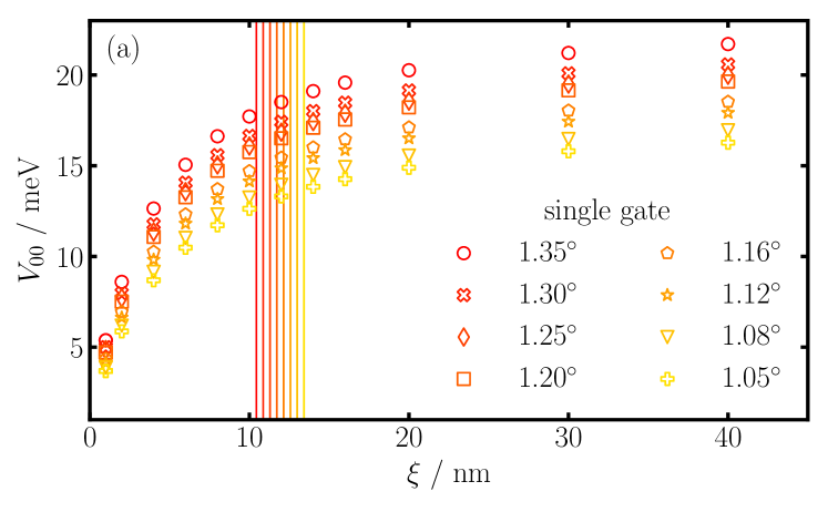
Fig. A1 shows the variation of the Hubbard parameters as a function of the separation of the gate(s) from the tBLG for a range of twist angles close to the magic angle. The panels on the left-hand (right-hand) side correspond to the single-gate (double-gate) device configuration. For the on-site Hubbard parameter [Figs. A1(a) and A1(b)], it is known that they scale linearly with the twist angle Goodwin et al. (2019a); Cao et al. (2018a). All twist angles, therefore, exhibit a similar dependence on the separation to the gate, but with the magnitude of scaled according to the twist angle.
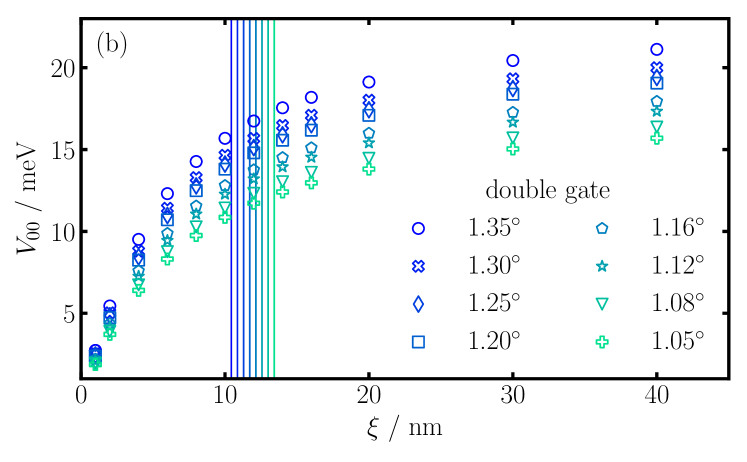
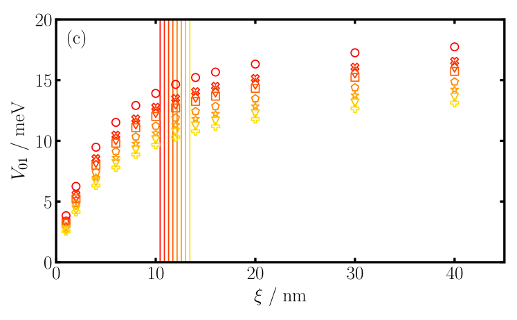
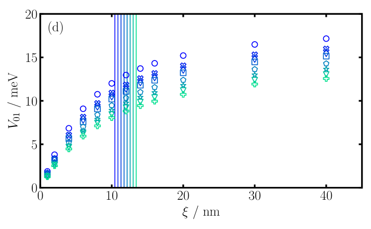
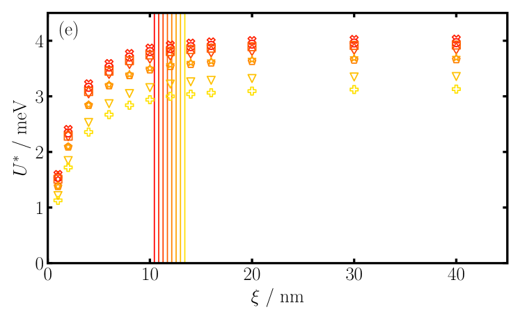
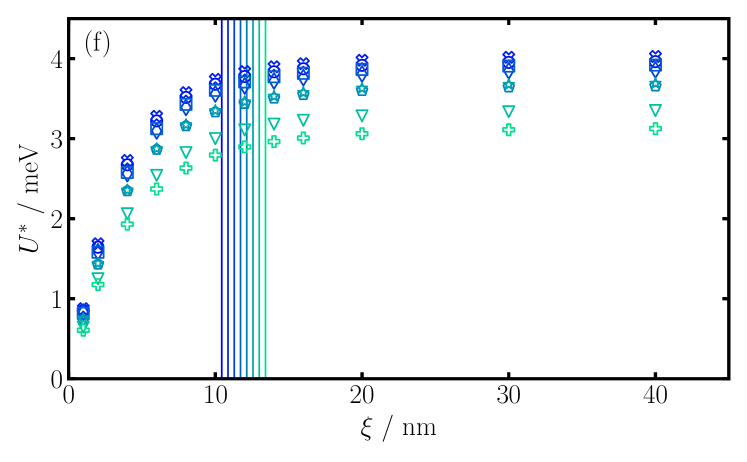
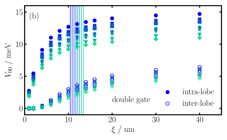
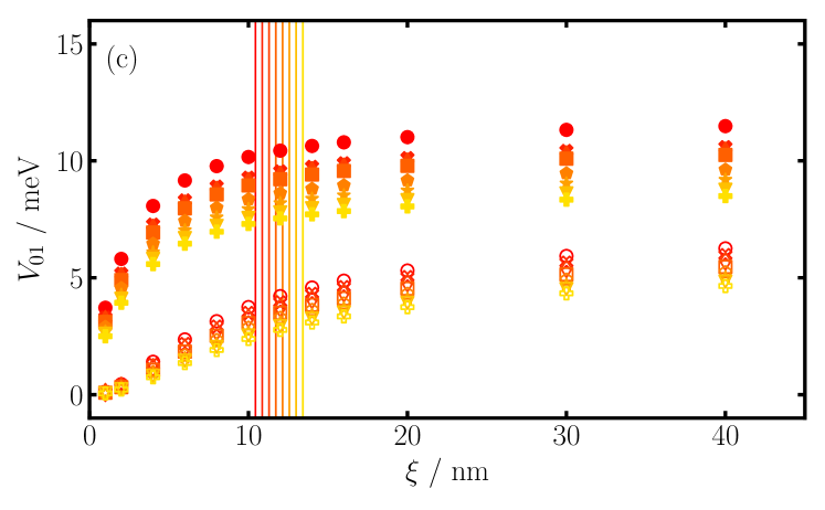
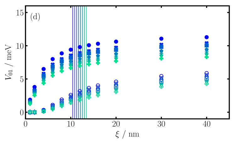
The nearest neighbour Hubbard parameter [Figs. A1(c) and A1(d)] and, therefore, also the long-ranged corrected on-site Hubbard parameter [Figs. A1(e) and A1(f)] have a similar dependence on the gate separation as the on-site Hubbard parameter . This similarity can be understood from the three-lobe structure of the Wannier functions Koshino et al. (2018); Kang and Vafek (2018b); Goodwin et al. (2019a, b): the predominant contribution to the Hubbard parameters comes from the overlap of lobes that are centred on the same moiré lattice site (“intra-lobe” contributions) plus contributions from the overlap of lobes centred on neighbouring moiré lattice sites (“inter-lobe” contributions) Koshino et al. (2018). In the case of the on-site parameter , there are three intra-lobe and six first-nearest neighbour inter-lobe interactions, whilst for the nearest neighbour parameter , there are two intra-lobe interactions, six first-nearest neighbour inter-lobe interactions and one second nearest-neighbour inter-lobe interaction.
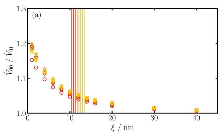
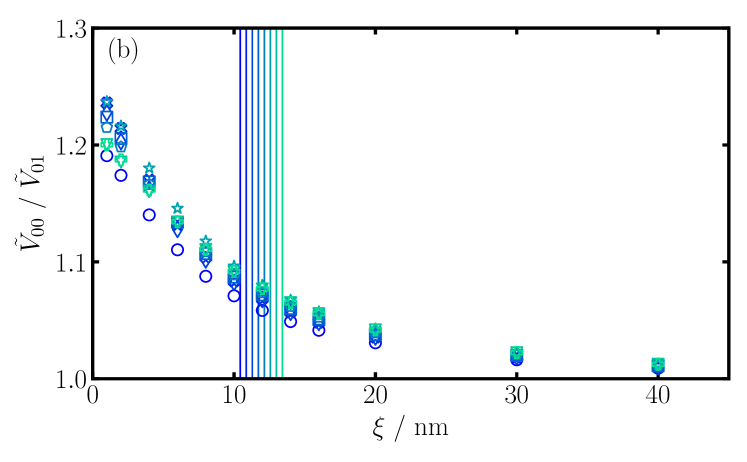
To make the larger reduction of compare to more explicit, in Fig. A2 we display the on-site Hubbard parameter in units of the on-site Hubbard parameter in the Coulomb limit, , over the next nearest Hubbard parameter in units of the next nearest Hubbard parameter in the Coulomb limit, ; again the subfigures are as a function of distance to the gate and all the studied twist angles are shown, with (a) corresponding to the single gate device and (b) to the double gate device. It is evident from this plot that increases as the distance to the gate is reduced. Therefore, (which also means ) is decreasing more than (and therefore ).
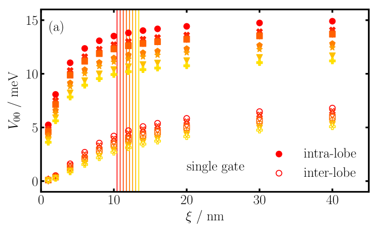
Fig. A3 shows the inter- and intra-lobe contributions to and for both device configurations [(a) and (c): single-gate; (b) and (d): double-gate]. These contributions were calculated from the method suggested in Ref. 30, but where the image-charge potential was used in place of the Coulomb potential Goodwin et al. (2019a). As can be seen, the intra-lobe contributions are larger than the inter-lobe contributions for all cases Goodwin et al. (2019a). As the distance to the gate is reduced (for separations around the moiré length scale), the inter-lobe contributions are suppressed more than the intra-lobe contributions. At separations much smaller than the moiré length scale, the intra-lobe contributions are significantly truncated.
Appendix B Critical gate separation for the double-gate configuration
In Fig. B1 we show the critical gate separation for the double gate as a function of twist angle from the magic angle. The plots are qualitatively similar to those of the single-gate configuration (Fig. 3). These plots were made by interpolating linearly in and with cubic splines in . We also fitted , where is the bandwidth of the flat bands from our tight-binding model, with a cubic spline as a function of . The roots of were found as a function of and , where is the critical value of the interaction from Ref. 36 (which is different for each value of the doping), and is the hopping parameter of graphene.

Appendix C Critical gate separation phase diagram at higher temperature

