Temperature-induced nanostructural evolution of hydrogen-rich voids in amorphous silicon: A first-principles study
Abstract
The paper presents an ab initio study of temperature-induced nanostructural evolution of hydrogen-rich voids in amorphous silicon. By using ultra-large a-Si models, obtained from classical molecular-dynamics simulations, with a realistic void-volume density of 0.2%, the dynamics of Si and H atoms on the surface of the nanometer-size cavities were studied and their effects on the shape and size of the voids were examined using first-principles density-functional simulations. The results from ab initio calculations were compared with those obtained from using the modified Stillinger-Weber potential. The temperature-induced nanostructural evolution of the voids was examined by analyzing the three-dimensional distribution of Si and H atoms on/near void surfaces using the convex-hull approximation, and computing the radius of gyration of the corresponding convex hulls. A comparison of the results with those from the simulated values of the intensity in small-angle X-ray scattering of a-Si/a-Si:H in the Guinier approximation is also provided, along with a discussion on the dynamics of bonded and non-bonded hydrogen in the vicinity of voids.
I Introduction
Amorphous silicon and its hydrogenated counterpart have a wide range of applications, from photovoltaics to thin-film technology. J. Thompson and C.Tuan (1987); A. Street (2000) Thin films of hydrogenated amorphous silicon (a-Si:H) are extensively used for passivation of crystalline silicon (c-Si) surfaces, which is essential to produce a high open-circuit voltage in silicon-based heterojunction solar cells. De Wolf et al. (2012); Kanevce and Metzger (2009) The passivation of Si dangling bonds by H atoms in the vicinity of a-Si:H/c-Si interfaces plays a key role in improving the properties of silicon heterostructures. Zeman and Zhang (2012) Post-deposition annealing is routinely used for structural relaxation of a-Si:H samples and incorporation of hydrogen at the a-Si:H/c-Si interfaces. The presence of hydrogen to an extent thus is often preferred Ge et al. (2012) for the preparation of a-Si:H samples with good interface properties. Experimental studies, such as spectroscopic ellipsometry Fujiwara et al. (2001); Collins et al. (2003) and Raman spectroscopy Daxing et al. (2003), indicate that, although the presence of nanometer-size voids can degrade the electronic quality of the samples, a small concentration of voids can improve the degree of surface passivation. This is generally believed to be due to the presence of mobile H atoms in a void-rich environment, where hydrogen can reach a-Si:H/c-Si interfaces, via diffusion or other mechanisms, in comparison to dense a-Si:H samples.
Heat treatment or annealing is an effective tool for nanostructural relaxation of laboratory-grown samples. Annealing at low to medium temperature (400–700 K) can considerably improve the quality of as-deposited samples, by removing unwanted impurities and reducing imperfections (e.g., defects) in the samples. Macco et al. (2017) For amorphous materials, annealing also increases the degree of local ordering in the amorphous environment. Earlier studies by small-angle X-ray scattering (SAXS) reported the presence of columnar-like geometric structure L. Williamson et al. (1994) and blister formation in annealed samples of a-Si:H. Serényi et al. (2013) Likewise, experiments on a-Si/a-Si:H, using positron-annihilation lifetime spectroscopy, have indicated that annealing above 673 K can lead to the formation of voids via vacancy clustering, which affects the nanostructural properties of the network. Sekimoto et al. (2016); Britton et al. (2001) It has been suggested that at higher temperature, near 800 K, a considerable restructuring can take place in the vicinity of the void boundary that can modify the shape and size of the voids. Young et al. (2007) Although tilting SAXS Young et al. (2007); L. Williamson et al. (1989) can provide some information on the geometrical shape of the voids, a direct experimental determination of annealing effects on the morphology of voids in the amorphous environment is highly nontrivial, as scattering experiments generally provide integrated or scalar information on the size and shape of the voids. By contrast, computational modeling can yield reliable structural information on the morphology of voids, Biswas and Elliott (2015); Biswas et al. (2017) provided that high-quality ultra-large models of a-Si/a-Si:H – with a linear dimension of several nanometers – are readily available and accurate total-energy functionals to describe the atomic dynamics of Si and H atoms are in place. However, despite numerous studies on computational modeling of a-Si and a-Si:H over the past several decades, there exist only a few computational studies Biswas et al. (1989); Brahim and Chehaidar (2013); Biswas et al. (2014); Biswas and Elliott (2015); Biswas et al. (2017) that truly attempted to address the structure and morphology of voids on the nanometer length scale in recent years.
The purpose of the present study is to conduct ab initio simulations of hydrogen-rich voids in ultra-large models of a-Si at low and high annealing temperatures. We are particularly interested in the structural reconstruction of the void surfaces, induced by annealing, and the resulting effects on the intensity in small-angle X-ray scattering (SAXS). Further, we intend to study the evolution of the shape of voids with temperature in the presence of hydrogen inside the voids. To this end, we develop significantly large models of a-Si, which are characterized by realistic distributions of voids as far as the results from SAXS, Muramatsu et al. (1992); L. Williamson et al. (1989) nuclear magnetic resonance (NMR), Boyce and Stutzmann (1985) infrared (IR), Chabal and Patel (1984); von Keudell and Abelson (1997) and positron-annihilation He et al. (1986) measurements are concerned. The term realistic here refers to the fact that the models must be able to accommodate nanometer-size voids with a void-volume fraction of 0.2–0.3%, as observed in SAXS, IR, and NMR measurements. The three-dimensional shape of the voids are studied by using the convex-hull approximation Biswas and Elliott (2015) of the boundary region of the voids, upon annealing at 300 K and 800 K, and the effects of the shape and size of the voids on the simulated SAXS intensity from the models are examined. The presence of molecular hydrogen and the statistics of various silicon-hydrogen bonding configurations near the void surfaces are also examined by introducing H atoms within the voids, with a number density of hydrogen (inside cavities) as observed in infrared spectroscopy and NMR measurements. Graebner et al. (1984); Chabal and Patel (1984)
The rest of the paper is as follows. In sec. II, we briefly describe the simulation of ultra-large models of a-Si with a linear dimension of a few tens of nanometers and the generation of nanometer-size voids in the resulting models in order to incorporate a realistic distribution of voids, with a void-volume fraction as observed in SAXS and IR measurements. Section III discusses the results of our work, with particular emphasis on the three-dimensional shape and size of the voids upon annealing at 300 K and 800 K. The correlation between the three-dimensional shape and size of the voids and the intensity of SAXS from simulations is discussed here. This is followed by a discussion on the motion of hydrogen in the vicinity of the voids, using ab initio molecular-dynamics (AIMD) simulations. This is followed by the conclusions in sec. IV. Finally, a comparison of the results with those from positron-annihilation lifetime (PAL) spectroscopy Sekimoto et al. (2016) and Doppler-broadening positron-annihilation spectroscopy (DB-PAS) Melskens et al. (2017) are presented.
II Computational Methods
II.1 Generation of ultra-large models of a-Si
We began by generating an ultra-large model of amorphous silicon in order to be able to study the intensity due to SAXS in the small-angle region of scattering wavevector Å-1. Since the key purpose of the study is to examine the structural evolution of the voids in a-Si on the nanometer length scale, by joint analyses of simulated SAXS intensities and three-dimensional distributions of atoms near void surfaces, it is necessary to simulate a sufficiently large model that can accommodate a realistic distribution of nanometer-size voids with the correct void-volume fraction, in the range from 0.01% to 0.3%, as observed from SAXS and IR measurements. Young et al. (2007); L. Williamson et al. (1989) Toward this end, a model a-Si network, consisting of 262,400 atoms, was generated using classical molecular-dynamics (MD) simulations, followed by geometry relaxation, by employing the modified Stillinger-Weber potential. Vink et al. (2001); Stillinger and Weber (1985) The initial configuration was obtained by randomly generating atomic positions in a cubic box of length 176.123 Å, which corresponds to the experimental mass density, 2.24 g.cm-3, of a-Si. Custer et al. (1994) Thereafter, constant-temperature MD simulations were performed using a chain of Nosé-Hoover thermostats Nosé (1984); Hoover (1985) and a time step of = 1 fs. During the MD runs, the system was heated to a temperature of 1800 K for 10 ps, and then it was cooled from 1800 K to 300 K at the rate of 10 K/ps. The heating-cooling cycle was carried out for at least 20 iterations. For each cycle, structural properties of the system, such as the coordination-number statistics, the bond-angle distribution, and the structure factor of the evolving configurations were examined. The procedure continues until it satisfies the convergence criteria that entail imposing a restriction on the upper limit of the root-mean-square (RMS) width of the bond-angle distribution (∘) and the coordination-defect density (of 3% or less) in the network. It may be noted that these variables are in conflict with each other, meaning that one can be reduced at the expense of increasing the other, and vice versa. Thus, care was taken to ensure that these criteria were simultaneously satisfied. Once the structural properties satisfied the aforementioned convergence criteria, the MD run was terminated and the system was relaxed by minimizing the total energy of the system with respect to the atomic positions. The resulting configuration was then used as a structural basis for the generation of additional models of a-Si by introducing voids in the network. The details of the simulation procedure can be found in Ref. Atta-Fynn and Biswas, 2018.
II.2 Void geometry and distribution in a-Si
Having obtained an ultra-large model of a-Si, we proceed to generate a realistic distribution of voids. Since computational modeling of void formation in a-Si, by mimicking the actual deposition and growth processes, is highly nontrivial, we generated a void distribution using experimental information on the shape, size, and the number density of voids. Experimental data from an array of measurements, such as small-angle scattering (SAS), D’Antonio and Konnert (1979); Muramatsu et al. (1992); L. Williamson et al. (1989); C Wright et al. (2007) infrared (IR) spectroscopy, Chabal and Patel (1984) nuclear magnetic resonance (NMR), Boyce and Stutzmann (1985) positron-annihilation lifetime (PAL) spectroscopy, He et al. (1986) and calorimetry measurements, Conradi and Norberg (1981); Graebner et al. (1984); Löhneysen et al. (1984) suggest that the linear size of the voids in a-Si typically lies between 10 Å and 40 Å and that the void-volume fraction can range from 0.01% to 0.3% of the total volume, depending upon the growth process, deposition rate, and the consequent electronic quality of the samples. Following these observations, we constructed a void distribution in the ultra-large model with the following properties: a) the voids are spherical in shape and have a diameter of 12 Å; b) the number density of the voids corresponds to a void-volume fraction of 0.2%; c) the voids are sparsely and randomly distributed, so that the distance between any two void centers is significantly larger than the dimension of the voids.
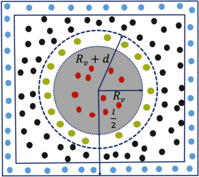
Figure 1 shows an example of a void embedded in a two-dimensional amorphous network. The void region is indicated by the gray circle of radius , which is surrounded by a layer of Si atoms (yellow) with a thickness . Silicon atoms in the layer constitute the surface/wall of the void, which we shall refer to as the void-surface atoms. The remaining Si atoms, within the cubic box (of length ), will be referred to as bulk Si atoms and are indicated as black and blue circles. To study the effect of hydrogen on the evolution of void surfaces, H atoms were introduced inside the voids so that no two H atoms were at a distance less than 1 Å from each other. The presence of H atoms in the network requires that the problem must be treated at the quantum-mechanical level using, for example, first-principles density-functional theory. However, given the size of the ultra-large model, such a task is hopelessly difficult and computationally infeasible, and an approximation of some sort is necessary. Here, we employed the local approach to electronic-structure calculations by invoking the principle of nearsightedness of an equilibrium system, as proposed by Kohn, Kohn (1996) and address the problem by studying an appropriately large sub-system, defined by a cubical box of length surrounding each void (see Fig. 1). Following an (approximate) invariance theorem on electronic structure of disordered alloys, due to Heine and coworkers, Ehrenreich et al. (1980); Haydock et al. (1975) the quantum local density of states near the voids is essentially independent of the boundary conditions at a sufficiently large distance, bou for example, the presence of a fixed layer of Si atoms on the edge of the box. Referring to Fig. 1, we chose = 6 Å, = 3 Å, and = 36 Å. To ensure that the void-volume fraction is consistent with the experimentally observed value of 0.01%–0.3%, we created 12 voids, reflecting a void-volume fraction of 0.2%, which were randomly distributed in the ultra-large model. An outer layer of Si atoms (blue) of thickness 3 Å was held fixed at the edge of the box of length for each void during first-principles simulations and total-energy relaxation of the sub-system so that the latter can be put back into the original ultra-large model for the calculation of the SAXS intensity, upon completion of annealing and geometry relaxation without boundary perturbations. Each sub-system, consisting of a cubical box of length 36 Å with a central void region of radius 6 Å, contained about 2200 atoms. The size of the cubical box was chosen carefully so that the local structural and electronic properties of the atoms in the vicinity of void surfaces were not affected by a fixed layer of atoms on the edge of the box, at a distance of 12 Å from the void surfaces. Care was also taken to ensure that the centers of the voids were sparsely distributed in the original ultra-large model so that the individual boxes or supercells did not overlap with each other. To study the effect of hydrogen on void surfaces, each void was loaded with 30 H atoms, as observed in IR and NMR measurements.H2_ The initial distributions of the H atoms were generated to satisfy the following two criteria: a) the H atoms were randomly distributed so that no two H atoms were separated by a distance less than 1 Å; b) the distance between any H atoms inside a void and a Si atom on the void surface was greater than or equal to 2 Å. The latter was achieved by confining the H atoms within a sphere of radius 4 Å from the center of the void. These criteria prevent the system from developing a sudden large force on light H atoms and an instantaneous formation of silicon-hydrogen bonds on void surfaces at the beginning of ab initio molecular-dynamics (AIMD) simulations.
II.3 Ab initio simulations of voids in a-Si
In the preceding section, we have generated a number of models (supercells/subsystems), containing as many as 2200 atoms and a central void of radius 6 Å, using the modified Stillinger-Weber (SW) potential. However, since the SW potential may not accurately describe the chemistry of silicon surfaces, it is necessary to treat these models using a first-principles total-energy functional from density functional theory (DFT) in order to reduce artifacts, such as the number of excessive dangling bonds or defects, associated with the SW-generated void surfaces. The standard DFT protocol here is to compute the self-consistent-field (SCF) solution of the Kohn-Sham (KS) equation, and the presence of voids or inhomogeneities in the system suggests that the generalized gradient approximation (GGA) should be employed in order to deal with the atomic density fluctuations near void surfaces. However, it is simply not feasible to solve the KS equations self-consistently for a problem of this size (i.e., about 2,200 atoms) and complexity using the existing plane-wave-based/local-basis DFT methodology. In particular, the computational cost for conducting SCF AIMD runs for several picoseconds is prohibitively large, even for a single configuration. To reduce the computational complexity of the problem, it is thus necessary to employ a suite of approximations for solving the KS equation. Here, we invoke the non-self-consistent Harris-functional approach Harris (1985); Zaremba (1990) in the local density approximation (LDA), using a minimal set of basis functions for Si atoms. While these approximations may affect the accurate determination of some aspects of the electronic structure of void surfaces, the results from test calculations on 1000-atom models with a void of radius 5 Å, obtained via the full SCF procedure for solving the KS equation in the LDA and GGA, indicate that the structural properties of the void surfaces in a-Si are minimally affected by these approximations. A discussion on the accuracy and computational efficiency of the Harris-functional approach to treat bulk a-Si and a-Si:H can be found in Ref. Atta-Fynn et al., 2004.
Ab initio calculations and total-energy optimization were conducted using the first-principles density-functional code Siesta. Soler et al. (2002) The latter employs a localized basis set and norm-conserving Troullier-Martins pseudopotentials, Troullier and Martins (1991) which are factorized in the Kleinman-Bylander Kleinman and Bylander (1982) form to remove the effect of core electrons. Electronic and exchange correlations between electrons are handled using the LDA, by employing the Perdew-Zunger parameterization of the exchange-correlation functional. Perdew and Zunger (1981) As stated earlier, we employed the Harris-functional approach Harris (1985); Zaremba (1990) that involves the linearization of the Kohn-Sham equations for structural relaxation and AIMD simulations. The latter were conducted over a period of 10 ps, with a time step of 1 fs. Single-zeta (SZ) and double-zeta-polarized (DZP) basis functions were employed for Si and H, respectively. Here, SZ functions correspond to one and three orbitals for Si atoms, whereas DZP functions refer to two and three orbitals for H atoms. The size of the simulation box or supercell is large enough in this work so that the Brillouin zone collapses onto the point, which was used for the Brillouin-zone sampling.
II.4 Simulation of SAXS intensity and void-size determination
The SAXS intensity for a binary system can be expressed with the aid of the partial structure factors and the atomic form factors of the constituent atoms. For a binary system, the scattering intensity, , can be expressed as, Cusack (1987)
| (1) |
where
| (2) |
is the partial structure factor associated with the atoms of type and such that , and is the partial pair-distribution function. Here, and are the atomic fraction and the atomic form factor of the atoms of type , respectively. In Eq. (2), the partial pair-distribution function, , is defined as , where is the average number density of atoms of type , , and . Once the scattering intensity is available, either numerically or experimentally, the size of the voids, or any extended inhomogeneities, can be estimated by invoking the Guinier approximation Guinier et al. (1995) in the small-angle limit, ,
| (3) |
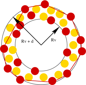
where is the characteristic size of the inhomogeneities in the dilute concentration limit. While Eq. (3) provides a reasonable estimate of void sizes from experimental data, difficulties arise in extracting the value from a - plot in simulations, owing to the finite size of the models. Since the effective small-angle region of is approximately given by , where is the linear dimension of the sample, a sufficiently large model is needed in order to obtain the mean value of , via averaging over several independent configurations. However, it has been observed Paudel et al. (2018) that, even for very large models, the lower limit of cannot be reduced arbitrarily by increasing due to the presence of noise in beyond 25–30 Å. The term in Eq. (2) for 25 Å introduces artifacts in for small values of , which make it difficult to accurately compute from the simulated intensity data. This necessitates the construction of alternative measures of void sizes and shapes directly from the distribution of atoms in the vicinity of voids. A simple but effective measure is to compute the gyrational radius from the distribution of the atoms on void surfaces between radii and , where is the void radius and is the width of the void surface, as discussed in sec. IIB. This is schematically illustrated in two dimensions in Fig. 2, where the positions of the void-surface atoms before and after annealing are shown in yellow and red colors, respectively. Assuming that the void-surface atoms (yellow) can displace, in the mean-square sense, from their initial position by during annealing, the radius of gyration, , for the assembly of void atoms (red) can be expressed as,
| (4) |
Here, and are the position of the atom and the center of mass of void-surface atoms, respectively. The atoms on the reconstructed surface are distributed within a spherical region of radius and is the Heaviside step function that asserts that only the atoms with contribute to .
| ( Å) | (g.cm-3) | (Å) | ||||
|---|---|---|---|---|---|---|
Here, we chose a value of = 1.5 Å for Si atoms in order to define the boundary of a reconstructed void surface. Since annealing at high temperature can introduce considerable restructuring of void surfaces, it is often convenient to invoke a suitable convex approximation to estimate the size and shape of the voids. Here, we employ the convex-hull approximation that entails constructing the minimal convex polyhedron that includes all the void-surface atoms on the boundary. The size of the convex region can be expressed as the radius of gyration of the convex polyhedron, or convex hull,
| (5) |
In Eq. (5), is the number of atoms (or vertices) that defines the convex polyhedral surface, and is the center of mass of the polyhedron. To determine the degree of deviation of the shape of a (convex) void from an ideal sphere, we employ the convex-hull volume () and surface area () and obtain the sphericity parameter,Wadell (1935)
| (6) |
The definition above is frequently used to measure the shape and roundness of sedimentary quartz particles, and it expresses the ratio of the surface area of a sphere to that of a non-spherical particle having an identical volume. Wadell (1935) It may be noted that a highly distorted void may not be accurately represented by a convex polyhedron and that the convex-hull volume provides an upper bound of the actual void volume, leading to . Likewise, as observed by Porod G. Porod and Kratky (1982), the value obtained from the Guinier approximation may not be accurate for very anisometric voids.
III Results and Discussion
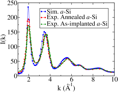
Before addressing the temperature-induced nanostructural changes in voids, we briefly examine the ultra-large model of a-Si, developed in sec. IIA, in order to validate its structural properties. Figure 3 shows the simulated values of the X-ray scattering intensity, along with the experimental values of the intensity for as-implanted (green) and annealed (red) samples of pure a-Si, reported by Laaziri et al. Laaziri et al. (1999) The simulated values closely match with the experimental data in Fig. 3, especially for the annealed samples, in the wide-angle region from 1 Å-1 to 10 Å-1 and beyond. Some characteristic structural properties of the ultra-large model are also listed in Table 1. Together with the X-ray intensity, the average bond angle and its deviation, 109.23∘ 9.26∘, and the number of four-fold-coordinated atoms, 97.6%, suggest that the structural properties of the model obtained from classical molecular-dynamics simulations in sec. IIA are consistent with experimental results. It may be reasonably assumed that the presence of a small amount of coordination defects ( 2.4%), which involve a length scale of 2–3 Å and are sparsely distributed in the amorphous environment, would not affect the scattering intensity appreciably in the small-angle region of the scattering wavevector. def A minor deviation in the height of the first peak in the simulated data in Fig. 3 from experimental values can be attributed in part to the use of the classical SW potential and partly to the large size of the model. A discussion on the validation of the structural properties of these models can be found in Ref. Atta-Fynn and Biswas, 2018.
III.1 Structural evolution of voids in a-Si at 300 K and 800 K
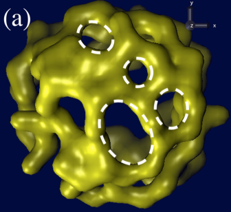
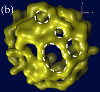
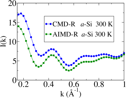
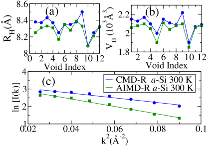
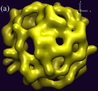
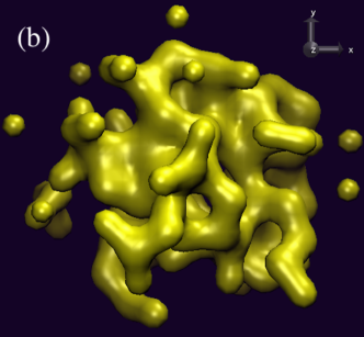
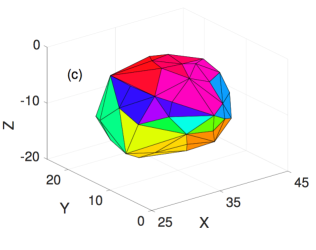
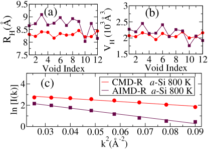
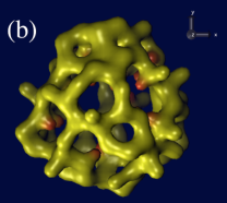
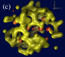
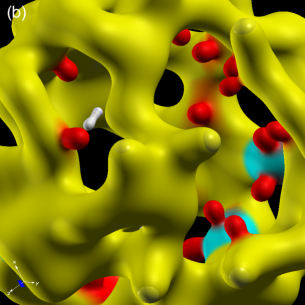
In this section, we discuss the three-dimensional shape and size of the voids in pure a-Si obtained from classical and quantum-mechanical annealing of the system at 300 K and 800 K, followed by total-energy optimization. Starting with an examination of the classical- and ab-initio-generated void surfaces, we analyze the computed SAXS spectrum obtained from the ultra-large model, which is embedded with the supercells containing voids annealed at 300 K and 800 K. Figure 4 shows the structure of a representative void (V3) after thermalization at 300 K for 10 ps, using classical and ab initio MD simulations. The void surface shown in Fig. 4 corresponds to a Gaussian-convoluted isosurface from the Xcrysden package.Kokalj (1999) The surface has been generated by placing a three-dimensional Gaussian function at the center of each atom and ensuring that the function has a value of 2.0 and 1.0 at the center and on the surface of the atom, respectively. By choosing an appropriate isovalue, between 0 to 2, and a suitable radius for Si atom, from standard crystallographic databases, it is possible to examine the morphological changes of voids, associated with the structural relaxation of the void-surface atoms at different temperature. A close examination of Figs. 4(a) and 4(b) suggests that the resultant structures are very similar to each other as far as the void surfaces are concerned, except for small changes as indicated by white rings. A similar observation has been made for the remaining voids as well, which showed very little changes on the void surfaces. These results are consistent with the variation of the simulated intensity shown in Fig. 5. A somewhat more pronounced scattering from the classically-treated voids (CMD-R) in comparison to the ab-initio-treated voids (AIMD-R) can be attributed to a minor expansion of the voids during classical simulations. This is clearly evident from Figs. 6(a) and 6(b), where the radius of gyration and the volume of the voids, respectively, are obtained from the convex-hull approximation of the void region. The polyhedral radii () for the voids from classical simulations were found to be consistently larger than the corresponding radii from ab initio simulations in Fig. 6(a). A similar conclusion applies to polyhedral volumes (), which are plotted in Fig. 6(b). Once the linear size, area, and volume of the voids are available in the convex approximation, the sphericity of voids, , can be determined from Eq. (6). A further measure of the size of the voids follows from the variation of the SAXS intensity, , with the wavevector, , in the small-angle region. By invoking the Guinier approximation (see Eq. 3), the Guinier radius, , can be obtained from vs. plots. Figure 6(c) shows the Guinier fits in the wavevector range, 0.15 Å 0.3 Å, which resulted in an value of 6.38 Å for the CMD-R model and 8.07 Å for the AIMD-R model. It should suffice to mention that the computation of the Guinier radius, , is affected by the limited data in the small-angle region of the intensity spectrum even for our large model and thus it may vary from the estimate obtained from the convex approximation.
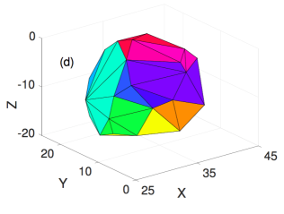
Having studied the microstructure of voids at 300 K, we now examine the structure of voids at the high temperature of 800 K. Figure 7 shows the shape of a representative void (V3) after annealing at 800 K from classical and ab initio MD simulations. A comparison between the two structures in Figs. 7(a) and 7(b) shows the regions on the two surfaces with a varying degree of reconstruction. The shape of the respective void surfaces obtained from using the convex-hull approximation is also shown in Figs. 7(c)-(d). Table 2 lists some of the parameters that characterize the void geometry in terms of the convex-hull radius (), the radius of gyration of the void-surface atoms (), the Guinier radius (), the hull volume (), and the average sphericity of the voids () after annealing at 300 K and 800 K. Although these scalar parameters do not vary much in the convex approximation, it is evident from the isosurface representation of the void in Figs. 7(a) and 7(b) that classical results noticeably differ from ab initio results, indicating the limitation of the classical force field in describing the restructuring of void surfaces at high temperature, namely at 800 K. This observation is also reflected in Figs. 8a-c, where the convex-hull radii, the hull volumes, and the intensity of SAXS at 800 K, respectively, are presented.
| Models | |||||
| a-Si (without hydrogen in voids) | |||||
| CMD-R300 | 7.60 | 8.34 | 6.38 | 2100 | 0.66 |
| AIMD-R300 | 7.55 | 8.28 | 8.07 | 2040 | 0.67 |
| CMD-R800 | 7.56 | 8.31 | 6.57 | 2080 | 0.63 |
| AIMD-R800 | 6.84 | 8.67 | 9.48 | 2250 | 0.68 |
| a-Si (with hydrogen in voids) | |||||
| AIMD-R300 | 6.66 | 8.36 | 8.66 | 2120 | 0.56 |
| AIMD-R800 | 6.61 | 8.76 | 10.01 | 2290 | 0.71 |
III.2 Structural evolution of hydrogen-rich voids in a-Si
Small-angle X-ray scattering measurements on HWCVD films indicate that the presence of preexisting H clusters can affect the nanostructure of voids due to H2 bubble pressure in the cavities, which, upon annealing, can lead to geometric changes, as observed via tilting SAXS and surface transmission electron microscopy (STEM).Young et al. (2007) Although the degree of such nano-structural changes may depend on the growth mechanism and the rate of film growth, it is instructive to address the problem from a computational viewpoint using CRN models of a-Si with nanometer-size voids, which are characterized by an experimentally consistent void-volume fraction and clusters of H atoms inside the voids.
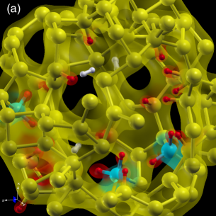
Figure 9 shows the structure of a hydrogen-rich nanovoid surface (of V3) obtained after annealing at 300 K and 800 K, followed by total-energy minimization. The evolution of Si and H atoms during annealing was described using ab initio density-functional forces and energies, from the local-basis DFT package Siesta. Soler et al. (2002) The procedure to conduct such AIMD simulations of voids, which are embedded in an ultra-large model of a-Si, has been described in sec. IIC.
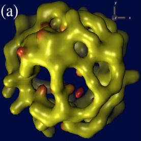
A comparison of Fig. 9(a) (with H atoms inside the void) with Fig. 4(b) (with no H atoms) reveals that the thermalization of the void (V3) and its neighboring region at 300 K does not introduce notable changes on the void surface, with the exception of the distribution of H atoms. The initial random distribution of H atoms, which was confined within a radius of 4 Å from the void center, evolved to produce several monohydrides (SiH) and a few dihydrides (SiH2), along with a few H2 molecules inside the cavity. The majority of H atoms continue to stay near the void at 300 K. By contrast, a considerable number of Si and H atoms have been found to be thermally driven out of the void region V3 at 800 K. An analysis of the distribution of Si atoms on the void surface, shown as yellow blob in Fig. 9, and H atoms (red) inside the void reveals that approximately 12.4% of the original Si atoms and 23.3% of the H atoms left the void region of radius 10.5 Å after annealing at 800 K. This is apparent from the isosurface plot in Fig. 9(b), where a considerable number of Si atoms can be seen to move away from the void-surface region, creating a somewhat diffused or scattered isosurface. This observation is found to be true for most of the other voids. On average, over 12 independent voids, approximately 8.3% of the Si atoms and 16.1% of the H atoms were found to leave the void regions at 800 K. By contrast, the corresponding average values for the same at 300 K for Si and H atoms are 0% and 2.6%, respectively. It thus follows that at 800 K the restructuring of a void surface can be considerably affected via thermal and H-induced motion of Si atoms, as well as through the formation of various silicon-hydrogen bonding configurations on void surfaces. Table 3 presents the statistics of various silicon-hydrogen bonding configurations in the vicinity of each void, which is defined by a radius of 10.5 Å.
| Void | Hiso | H2 | SiH | SiH2 | SiH3 | ||
|---|---|---|---|---|---|---|---|
| 300 K | |||||||
| V1∗ | 2 | 1 | 20 | 2 | 0 | 8.34 | 0.51 |
| V2 | 0 | 3 | 22 | 1 | 0 | 8.33 | 0.56 |
| V3 | 0 | 3 | 17 | 3 | 0 | 8.5 | 0.59 |
| V4 | 0 | 0 | 26 | 1 | 0 | 8.4 | 0.58 |
| V5 | 0 | 1 | 25 | 1 | 0 | 8.2 | 0.62 |
| V6∗ | 1 | 2 | 22 | 1 | 0 | 8.34 | 0.54 |
| V7 | 0 | 1 | 26 | 1 | 0 | 8.31 | 0.54 |
| V8 | 1 | 1 | 23 | 2 | 0 | 8.5 | 0.57 |
| V9 | 0 | 3 | 20 | 0 | 1 | 8.35 | 0.51 |
| V10∗ | 1 | 3 | 18 | 2 | 0 | 8.28 | 0.60 |
| V11 | 2 | 4 | 19 | 0 | 0 | 8.34 | 0.59 |
| V12 | 2 | 2 | 23 | 0 | 0 | 8.52 | 0.56 |
| 800 K | |||||||
| V1 | 0 | 0 | 20 | 2 | 0 | 8.36 | 0.90 |
| V2 | 0 | 2 | 20 | 2 | 0 | 8.84 | 0.66 |
| V3∗ | 1 | 2 | 16 | 1 | 0 | 9.07 | 0.79 |
| V4 | 0 | 1 | 23 | 1 | 0 | 8.64 | 0.62 |
| V5 | 0 | 0 | 20 | 2 | 0 | 8.95 | 0.70 |
| V6 | 0 | 2 | 14 | 1 | 1 | 8.67 | 0.83 |
| V7 | 0 | 3 | 14 | 3 | 0 | 8.94 | 0.64 |
| V8∗ | 1 | 1 | 14 | 3 | 0 | 8.95 | 0.73 |
| V9 | 0 | 1 | 22 | 1 | 0 | 9.07 | 0.62 |
| V10 | 0 | 1 | 21 | 2 | 0 | 8.71 | 0.62 |
| V11 | 2 | 3 | 15 | 1 | 0 | 8.38 | 0.81 |
| V12 | 1 | 0 | 21 | 2 | 0 | 8.56 | 0.56 |
| Temp. | Hiso | H2 | SiH | SiH2 | SiH3 | Ex-void |
|---|---|---|---|---|---|---|
| 300 K | 2.5 | 13.3 | 72.5 | 8.3 | 0.8 | 2.6 |
| 800 K | 1.4 | 8.9 | 61.1 | 11.7 | 0.8 | 16.1 |

To obtain the linear size of the voids, we computed the radius of gyration, , using Eq. (4). Likewise, the convex-hull approximation of a void region, defined by a set of void-surface atoms, provides the radius of the convex polyhedron, , from Eq. (5). Figure 10(a)-(b) shows the values of and the corresponding hull volumes, , of 12 voids, each of which has been computed upon annealing and geometry relaxation. Similarly, the values obtained from the real-space distribution of the void atoms are listed in Table 2. The apparent deviation of from can be attributed to the fact that the computation of involves all the atoms on the surface and interior regions of the voids, whereas the convex-hull approximation includes only those atoms on the void-surface region that define the minimal convex polyhedral volume. Thus, provides an upper bound of the radial size of the voids. In order to compare and values with the linear size of the voids from the simulated intensity plots in SAXS, we have invoked the Guinier approximation to estimate the Guinier radius, , from - plots, as shown in Fig. 10(c). Table 2 suggests that the values obtained from the simulated intensity plots reasonably match with the corresponding average values of at 300 K and 800 K. It may be noted that, while the intensity plot in Fig. 10(c) is not particularly sensitive to the shape of the voids, the slightly pronounced scattering in the region 0.05 Å-2 is possibly indicative of the expansion of the void volume at 800 K, as observed in the convex-hull volume in Fig. 10(b). The exact cause of this increased scattering intensity is difficult to determine but it appears that a combination of the pressure due to H2 bubbles, surface roughening of the voids, and the displacement of the atoms on the void surfaces at high temperature could lead to this additional scattering. This observation is corroborated by the experimental results from a small-angle X-ray scattering study of nanovoids in HWCVD amorphous Si films that indicated an increase of individual void volumes upon annealing at 813 K. Young et al. (2007)
III.3 Hydrogen dynamics near voids in a-Si
In this section, we shall make a few observations on the dynamics of hydrogen atoms in the vicinity of void surfaces from ab initio molecular-dynamics simulations. Since the mass of H atoms is significantly smaller than that of Si atoms, the motion of H atoms is more susceptible to the annealing temperature and, more importantly, to the resulting temperature-induced structural changes on the void surfaces. This is particularly noticeable at high temperature. Having established earlier that the structural changes on the void surfaces are more pronounced at 800 K, we shall now examine the character of hydrogen dynamics inside (and near the surface of) the voids at 800 K. Despite the limited timescale of the present AIMD simulations, spanning 10 ps only, it is reasonable to assume that, at high temperature, the dynamical character of hydrogen motion inside the voids would be reflected in the first several picoseconds. It may be noted that, unlike structural properties, the dynamics of hydrogen in a-Si may depend on the accuracy of total energies and forces from DFT calculations. The use of the Harris-functional approximation in the present work, in an effort to address the structure of voids on the nanometer length scale, suggests that the results on hydrogen dynamics presented here are somewhat approximate in nature. A full self-consistent-field DFT calculation, over a period of a few tens of picoseconds, using plane-wave or even local basis sets for 2200-atom models is computationally overkill and outside scope of the present work on nanostructural evolution.
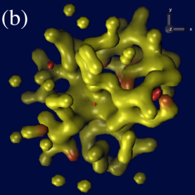
Figure 11(a) depicts the time evolution of hydrogen atoms at 800 K within two voids, V12 and V7. Initially, all hydrogen atoms/molecules were uniformly distributed inside the voids within a radius of 4 Å from the center of the voids (see Fig. 1). The mean-square displacements (MSD), , of hydrogen atoms – averaged over all H atoms in the respective void – are shown in Fig. 11(a) from 0 to 10 ps. The corresponding real-space distributions of Si and H atoms on the void surfaces and their immediate vicinity are also shown in Figs. 11(b) and 11(c) for V12 and V7, respectively. The early-time behavior of the dynamics, from 0 to 0.5 ps, can be roughly understood from elementary considerations. Given that the majority of H atoms are away from the void surface at the beginning of simulation, by at least 2 Å or more, the early-time behavior of the dynamics would be primarily determined by the temperature of the system for a reasonably well-defined initial H distribution. Since the root-mean-square (RMS) speed of H atoms at 800 K for the Maxwell-Boltzmann distribution is about 0.045 Å/fs, it would be reasonable to assume that the initial behavior can last for about a fraction of a picosecond, after which H atoms become affected by the presence of the void surface.
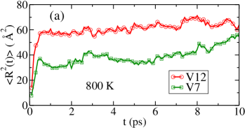
It is the marked difference in the value of in Fig. 11, from 1 ps to 8 ps, that we find most interesting. This notable difference between the two sets of MSD values beyond 0.5 ps can be understood by taking into account the real-space structure of the void surfaces. In addition to the trivial thermal and configurational fluctuations – caused by temperature and the disorder in H distributions, respectively – the motion of H atoms is also affected by the varying degree of re-structuring of Si atoms on the void surfaces after 0.5 ps. The surface structure of V7 can be seen to be more open or scattered compared to its counterpart in V12, which is more compact or well-defined, as shown in Figs. 11(c) and 11(b), respectively. This has been also confirmed by analyzing the distributions of void-surface atoms in the interior of V12 and V7. The presence of Si atoms inside V7 may reduce the effective diffusion rate of H atoms, due to additional scattering from interior Si atoms, during intermediate-time evolution from 1 ps onward. By contrast, the more well-defined void surface of V12, with few Si atoms inside, provides less resistance to H atoms during their intermediate-time evolution. Thus, hydrogen diffusion in V12 proceeds relatively uninterruptedly, in the presence of few Si atoms from void surfaces, leading to a notable difference in their MSD values during the first several picoseconds of simulations. This observation has been found to be true for other pairs of voids for which a notable difference in the MSD values exists. In view of our observation that the intermediate-time behavior (i.e., from 1 ps to 8 ps) of the H dynamics can be influenced by the roughness of void surfaces, it might be necessary to take into account the appropriate size and the accurate surface structure of the voids in the calculations. However, a full SCF study of hydrogen dynamics inside nanometer-size voids in a-Si for several tens of picoseconds is computationally prohibitive and outside the scope of the present study.
III.4 Silicon-hydrogen bonding configurations on void surfaces
Experimental data from positron-annihilation lifetime (PAL) spectroscopy, Sekimoto et al. (2016) Rutherford backscattering spectrometry (RBS), Sekimoto et al. (2018) and Fourier-transform infrared spectroscopy-attenuated total reflection (FTIR-ATR) Sekimoto et al. (2018) indicate that bonded and non-bonded hydrogens play an important role in characterizing the structural and optical properties of a-Si:H. Sekimoto et al. Sekimoto et al. (2016, 2018) recently demonstrated that the presence of non-bonded hydrogens (NBH) at concentrations beyond 2.8 at. % in amorphous silicon networks led to changes in the vacancy-size distribution and induced formation of nanometer-size voids in the network via relaxation of internal stress. The formation of H2 molecules and their evolution can be probed by an analysis of the low-temperature (LT) peak of the hydrogen-effusion profile Sekimoto et al. (2016); Beyer (1991, 2003) near 750 K, whereas the number density of H2 molecules can be estimated from the collision-induced weak IR absorption in the frequency region of 4100 cm-1 to 5500 cm-1. Chabal and Patel Chabal and Patel (1984) reported a value of H2/cm3 by analyzing data obtained from IR measurements at room temperature. Although the present study, based on pure a-Si networks, does not permit us to address the crucial role of silicon-hydrogen bonding configurations in a-Si:H in general, it does provide us with new insights into the role of bonded and non-bonded hydrogens in the vicinity of the walls of H-rich voids. Tables 3 and 4 list the statistics and the average concentration of various bonded and non-bonded hydride configurations inside the voids, respectively. Non-bonded hydrogens chiefly comprise H2 molecules, along with one or two isolated H atoms near the voids. The latter possibly originate from the short annealing time of 10 ps of AIMD simulations. The number of H2 molecules per void ranges from 0 to 4 and 0 to 3 at 300 K and 800 K, respectively, which translates into a density of 1.5–2.2 1021 H2/cm3 for nanometer-size voids. This value matches very well with the experimental value of 1021 H2/cm3 from IR measurements by Chabal and Patel, Chabal and Patel (1984) as mentioned earlier.
These results are also consistent with the reported data from RBS measurements. Sekimoto et al. (2016)
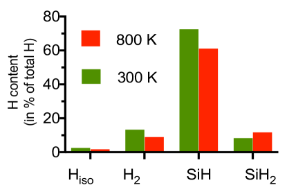
On the other hand, the great majority of bonded hydrogens appeared in monohydride (SiH) configurations. An examination of the local bonding environment of silicon atoms near the void surfaces showed that approximately 72.5 at. % and 61.1 at. % of total H atoms formed Si-H bonds at 300 K and 800 K, respectively (see Table 4). Of the remaining H atoms, about 8.3 % (11.7%) were found to be bonded with Si as SiH2 configurations at 300 K (800 K). Apart from a few isolated H atoms, the rest of the hydrogen has left the spherical void region of radius 10.5 Å. A graphic distribution of the presence of H2 molecules and the bonded SiH2 configurations on the wall of V3 at 300 K is depicted in Fig. 12. Several SiH2 configurations can be seen to have formed on the surface of the void. This observation is consistent with experimental results from infrared measurements Chabal and Patel (1984) and the recent computational studies based on information-driven atomistic modeling of a-Si:H. Biswas and Elliott (2015); Biswas et al. (2014) Figure 13 shows the concentration of hydrogen associated with various silicon-hydrogen bonding configurations. The results clearly establish that a considerable number of H2 molecules, of about 9–13% of the total H, can form in the vicinity of voids, depending upon the annealing temperature, concentration of H atoms, the source of hydrogen, and the preparation methods of a-Si samples.
IV Conclusions
In this paper, we studied the temperature-induced nano-structural changes of the voids in a-Si at low and high annealing temperature in the range 300–800 K using classical and quantum-mechanical simulations, in the absence and presence of hydrogen near voids. This was achieved by generating an ultra-large model of a-Si, consisting of more than 260,000 atoms, in order to be able to produce a realistic distribution of nanometer-size voids in the amorphous environment of Si atoms, as observed in SAXS, PAL, IR, and hydrogen-effusion measurements. An examination of the distribution of the atoms near the voids reveals that the reconstruction of void surfaces in pure a-Si at 300 K led to minimal changes in the shape and size of the voids, which can be readily understood from a classical treatment of the problem. By contrast, the high-temperature annealing at 800 K caused significant changes in the shape and size of the voids, with noticeable structural differences between classical and quantum-mechanical results. This observation appears to indicate that classical potentials, such as the modified SW potential, might not be particularly suitable for an accurate description of the dynamics of Si atoms near voids and the resulting reconstruction of the void surfaces at high temperatures.
An important outcome of the present study is that the dynamics of bonded and non-bonded hydrogens near the voids and the degree of void-surface reconstruction are found to be intrinsically related to each other. Ab initio annealing of a-Si networks with a void-volume fraction of 0.2% at 300 K and 800 K suggests that the presence of hydrogen within voids can facilitate surface reconstruction through the formation of silicon monohydride and dihydride configurations, as well as the displacement of Si atoms on the void surfaces. The rearrangement of atoms on void surfaces affects the diffusion of non-bonded hydrogens, which in turn produce surface bumps and changes the shape and size of the original void. This observation is reflected in the time evolution of hydrogen during annealing. The presence of Si atoms inside a heavily reconstructed fuzzy/rough void surface reduces the effective diffusion rate of hydrogen, due to additional scattering from the interior Si atoms, in their intermediate-time evolution from 1 ps onward. In contrast, a compact void surface provides less resistance to hydrogen during their evolution. Thus, hydrogen diffusion inside a smooth or well-defined void proceeds with little or no hindrance, leading to a notable difference in their mean-square-displacement (MSD) values during their intermediate-time evolution. Finally, the results from the study show the presence of bonded hydrogens (BH), mostly SiH, SiH2, and non-bonded hydrogens (NBH) in the form of H2 molecules. The concentration of BH and NBH found in our study is consistent with the experimental values obtained from infrared (IR), Rutherford back scattering (RBS), and hydrogen-forward scattering (HFS) measurements. An examination of the silicon-hydrogen bonding configurations near the voids suggests that the interior walls of the voids are decorated with SiH2, which is supported by experimental results from infrared and ellipsometric studies. Likewise, the concentration of H2 molecules obtained from the first-principles density-functional simulations in the present study is found to be consistent with the experimental value estimated from the collision-induced weak IR absorption by H2 molecules in the frequency region of 4100–5500 cm-1.
acknowledgements
This work was partially supported by the U.S. National Science Foundation under Grants No. DMR 1507166 and No. DMR 1507118. We acknowledge the Texas Advanced Computing Center at the University of Texas at Austin for providing HPC resources that have contributed to the results reported in this work. One of us (P.B.) thanks Prof. David Drabold (Ohio University) for discussions.
References
- J. Thompson and C.Tuan (1987) M. J. Thompson and H. C.Tuan, IEEE Aerospace and Electronic Systems Magazine 2, 25 (1987).
- A. Street (2000) R. A. Street, Technology and Applications of Amorphous Silicon, Springer Series in Materials Science, Vol. 37 (Springer-Verlag, 2000).
- De Wolf et al. (2012) S. De Wolf, A. Descoeudres, Z. Holman, and C. Ballif, Green 2, 7 (2012).
- Kanevce and Metzger (2009) A. Kanevce and W. K. Metzger, Journal of Applied Physics 105, 094507 (2009).
- Zeman and Zhang (2012) M. Zeman and D. Zhang, Heterojunction Silicon Based Solar Cells (Springer Berlin Heidelberg, 2012) pp. 13–43.
- Ge et al. (2012) J. Ge, Z. P. Ling, J. Wong, T. Mueller, and A. Aberle, Energy Procedia 15, 107 (2012).
- Fujiwara et al. (2001) H. Fujiwara, M. Kondo, and A. Matsuda, Physical Review B 63, 115306 (2001).
- Collins et al. (2003) R. Collins, A. Ferlauto, G. Ferreira, C. Chen, J. Koh, R. Koval, Y. Lee, J. Pearce, and C. Wronski, Solar Energy Materials and Solar Cells 78, 143 (2003).
- Daxing et al. (2003) H. Daxing, J. D. Lorentzen, J. Weinberg-Wolf, L. E. McNeil, and Q. Wang, Journal of Applied Physics 94, 2930 (2003).
- Macco et al. (2017) B. Macco, J. Melskens, N. Podraza, K. Arts, C. Pugh, O. Thomas, and W. Kessels, Journal of Applied Physics 122, 035302 (2017).
- L. Williamson et al. (1994) D. L. Williamson, S. J. Jones, and Y. Chen, NREL/TP-451-6395.UC Category 271. DE94006931 , 6395 (1994).
- Serényi et al. (2013) M. Serényi, C. Frigeri, Z. Szekrényes, K. Kamarás, L. Nasi, A. Csik, and N. Q. Khánh, Nanoscale Research Letters 8, 84 (2013).
- Sekimoto et al. (2016) T. Sekimoto, M. Matsumoto, A. Sagara, M. Hishida, and A. Terakawa, Journal of Non-Crystalline Solids 447, 207 (2016).
- Britton et al. (2001) D. T. Britton, A. Hempel, M. Härting, G. Kögel, P. Sperr, W. Triftshäuser, C. Arendse, and D. Knoesen, Physical Review B 64, 075403 (2001).
- Young et al. (2007) D. L. Young, P. Stradins, Y. Xu, L. M. Gedvilas, E. Iwaniczko, Y. Yan, H. M. Branz, Q. Wang., and D. L. Williamson, Applied Physics Letters 90, 081923 (2007).
- L. Williamson et al. (1989) D. L. Williamson, A. H. Mahan, B. P. Nelson, and R. S. Crandall, Journal of Non-Crystalline Solids 114, 226 (1989).
- Biswas and Elliott (2015) P. Biswas and S. R. Elliott, Journal of Physics: Condensed Matter 27, 435201 (2015).
- Biswas et al. (2017) P. Biswas, D. Paudel, R. Atta-Fynn, D. A. Drabold, and S. R. Elliott, Physical Review Applied 7, 024013 (2017).
- Biswas et al. (1989) R. Biswas, I. Kwon, A. M. Bouchard, C. M. Soukoulis, and G. S. Grest, Physical Review B 39, 5101 (1989).
- Brahim and Chehaidar (2013) R. Brahim and A. Chehaidar, Advances in Materials Physics and Chemistry 3, 19 (2013).
- Biswas et al. (2014) P. Biswas, D. A. Drabold, and R. Atta-Fynn, Journal of Applied Physics 116, 244305 (2014).
- Muramatsu et al. (1992) S. Muramatsu, S. Matsubara, T. Watanabe, T. Shimada, T. Kamiyama, and K. Suzuki, Journal of Non-Crystalline Solids 150, 163 (1992).
- Boyce and Stutzmann (1985) J. B. Boyce and M. Stutzmann, Physical Review Letters 54, 562 (1985).
- Chabal and Patel (1984) Y. J. Chabal and C. K. N. Patel, Physical Review Letters 53, 210 (1984).
- von Keudell and Abelson (1997) A. von Keudell and J. R. Abelson, Applied Physics Letters 71, 3832 (1997).
- He et al. (1986) Y. J. He, M. Hasegawa, R. Lee, S. Berko, D. Adler, and A.-L. Jung, Physical Review B 33, 5924 (1986).
- Graebner et al. (1984) J. E. Graebner, B. Golding, L. C. Allen, D. K. Biegelsen, and M. Stutzmann, Physical Review Letters 52, 553 (1984).
- Melskens et al. (2017) J. Melskens, S. W. H. Eijt, M. Schouten, A. S. Vullers, A. Mannheim, H. Schut, B. Macco, M. Zeman, and A. H. M. Smets, IEEE Journal of Photovoltaics 7, 421 (2017).
- Vink et al. (2001) R. L. C. Vink, G. T. Barkema, W. F. van der Weg, and N. Mousseau, Journal of Non-Crystalline Solids 282, 248 (2001).
- Stillinger and Weber (1985) F. H. Stillinger and T. A. Weber, Physical Review B 31, 5262 (1985).
- Custer et al. (1994) J. S. Custer, M. O. Thompson, D. C. Jacobson, J. M. Poate, S. Roorda, W. C. Sinke, and F. Spaepen, Applied Physics Letters 64, 437 (1994).
- Nosé (1984) S. Nosé, The Journal of Chemical Physics 81, 511 (1984).
- Hoover (1985) W. G. Hoover, Physical Review A 31, 1695 (1985).
- Atta-Fynn and Biswas (2018) R. Atta-Fynn and P. Biswas, Journal of Chemical Physics 148, 204503 (2018).
- D’Antonio and Konnert (1979) P. D’Antonio and J. H. Konnert, Physical Review Letters 43, 1161 (1979).
- C Wright et al. (2007) A. C Wright, A. C Hannon, R. N Sinclair, T. M Brunier, C. A Guy, R. J Stewart, M. B Strobel, and F. Jansen, Journal of Physics: Condensed Matter 19, 415109 (2007).
- Conradi and Norberg (1981) M. S. Conradi and R. E. Norberg, Physical Review B 24, 2285 (1981).
- Löhneysen et al. (1984) H. V. Löhneysen, H. J. Schink, and W. Beyer, Physical Review Letters 52, 549 (1984).
- Kohn (1996) W. Kohn, Physical Review Letters 76, 3168 (1996).
- Ehrenreich et al. (1980) H. Ehrenreich, F. Seitz, and D. Turnbull, Solid State Physics, v. 35 (Elsevier Science, 1980).
- Haydock et al. (1975) R. Haydock, V. Heine, and M. Kelly, Journal of Physics C: Solid State Physics 8, 2591 (1975).
- (42) Strictly speaking, the boundary must be located at a distance greater than the characteristic decay length of the density matrix of the system. The presence of an electronic gap in a-Si asserts that its density matrix Goedecker (1999) can be characterized by a well-defined decay length.
- (43) The rationale behind adding 30 H atoms inside the voids is based on calorimetry and infrared measurements, Chabal and Patel (1984) which suggest the presence of about 12 to 15 “bulk” H2 molecules inside nanometer-size voids.
- Harris (1985) J. Harris, Physical Review B 31, 1770 (1985).
- Zaremba (1990) E. Zaremba, Journal of Physics: Condensed Matter 2, 2479 (1990).
- Atta-Fynn et al. (2004) R. Atta-Fynn, P. Biswas, P. Ordejón, and D. A. Drabold, Physical Review B 69, 085207 (2004).
- Soler et al. (2002) J. M. Soler, E. Artacho, J. D. Gale, A. Garciá, J. Junquera, P. Ordejón, and D. Sánchez-Portal, Journal of Physics: Condensed Matter 14, 2745 (2002).
- Troullier and Martins (1991) N. Troullier and J. L. Martins, Physical Review B 43, 1993 (1991).
- Kleinman and Bylander (1982) L. Kleinman and D. M. Bylander, Physical Review Letters 48, 1425 (1982).
- Perdew and Zunger (1981) J. P. Perdew and A. Zunger, Physical Review B 23, 5048 (1981).
- Cusack (1987) N. E. Cusack, The Physics of Structurally Disordered Matter (Adam Hilger, 1987).
- Guinier et al. (1995) A. Guinier, G. Fournet, and K. L. Yudowitch, Small-angle scattering of X-rays (Wiley, New York, 1995).
- Paudel et al. (2018) D. Paudel, R. Atta-Fynn, D. A. Drabold, S. R. Elliott, and P. Biswas, Physical Review B 97, 184202 (2018).
- Wadell (1935) H. Wadell, The Journal of Geology 43, 250 (1935).
- G. Porod and Kratky (1982) O. G. Porod, edited by Glatter and O. Kratky, Small Angle X-ray Scattering (Academic Press, New York, 1982) pp. 17 – 51.
- Laaziri et al. (1999) K. Laaziri, S. Kycia, S. Roorda, M. Chicoine, J. L. Robertson, J. Wang, and S. C. Moss, Physical Review B 60, 13520 (1999).
- (57) The observation relies on the assumptions that the variation of the local mass density near the defect sites and the corresponding length scale of 2–3 Å, associated with a sparse distribution of isolated defects, would not be too large to induce additional scattering in the small-angle region of the scattering wavevector. Suffice it to mention that, for clustered defects, this may not be necessarily true. These assumptions have been verified computationally by creating artificial defects in 100% 4-fold-coordinated a-Si networks here.
- Kokalj (1999) A. Kokalj, Journal of Molecular Graphics and Modelling 17, 176 (1999).
- Sekimoto et al. (2018) T. Sekimoto, M. Matsumoto, and A. Terakawa, Japanese Journal of Applied Physics 57, 08RB07 (2018).
- Beyer (1991) W. Beyer, Physica B: Condensed Matter 170, 105 (1991).
- Beyer (2003) W. Beyer, Solar Energy Materials and Solar Cells 78, 235 (2003).
- Goedecker (1999) S. Goedecker, Review of Modern Physics 71, 1085 (1999).