Resist and Transfer Free Patterned CVD Graphene Growth on ALD Nano Layers
Abstract
Multilayer graphene (MLG) films were grown by chemical vapour deposition (CVD) on molybdenum carbide () substrates. We fabricated the catalytic films by plasma enhanced atomic layer deposition (PEALD). The mechanism of graphene growth is studied and analysed for amorphous and crystalline films. In addition, the unique advantages of catalytic substrate PEALD are demonstrated in two approaches to graphene device fabrication. First, we present a complete bottom up, resist-free patterned graphene growth (GG) on pre-patterned PEALD performed at 50. Selective CVD GG eliminates the need to pattern or transfer the graphene film to retain its pristine, as grown, qualities. Furthermore, we fabricated MLG directly on PEALD on 100 nm suspended SiN membrane. We characterise the MLG qualities using Raman spectroscopy, and analyse the samples by optical microscopy, scanning electron microscopy and X-ray diffraction measurements. The techniques of graphene device manufacturing demonstrated here pave the path for large scale production of graphene applications.
1 Introduction
Next generation graphene-based applications would require a resist and transfer free graphene growth in order to realise the promise of graphene for flexible electronics[1, 2], and sub 10nm nodes’ interconnects [3]. Graphene based interconnects would significantly reduce the RC delay and thermal budget which is currently the bottle neck in sub 10nm transistor nodes [4, 5] due to the excellent room temperature carrier mobility and thermal conductivity. However, graphene based devices exhibit far lower carrier mobility than the theoretical predictions promise. Encapsulation of graphene with lattice matching dielectric material such as hBN shows remarkable improvement, but performance is still subpar [6]. The main challenges of current commercial chemical vapour deposition (CVD) grown graphene are resist residue due to target transfer process [7, 8], and patterning of graphene, which degrade the graphene quality, resulting in the far lower carrier mobility than theoretical predictions. Known techniques include photolithography, ion beam milling [9], shadow masking [10], area selective passivation layer [11] and stencil mask [12]. Despite these tremendous efforts, the goal of a scalable, low cost, high quality patterned graphene using commercially available tools, has not been achieved. Photolithography methods leave resist residue, and ion beam etching causes broad lateral damage close to pattern area due to scattering ions [13, 14]. Patterning graphene with oxygen plasma inevitably oxides graphene edges [15], and the stencil mask poses resolution limitation . Furthermore, transfer of graphene from one substrate onto another degrades the graphene quality due to induced film compression and tension, and potential contamination between the graphene and target interfaces. A wholesome solution that avoids both the need to pattern the graphene or to transfer a pre patterned graphene onto a target, has yet to be introduced. While advancements have been made toward transfer free graphene grown on patterned Mo catalytic layer [16], resist residue on the underlying growth substrate cannot be fully removed. As defects, non uniformity and contamination will imminently translate to graphene defects, it is vital to achieve a resist free catalytic surface, in a uniform and conformal layer deposition. Atomic layer deposition (ALD) is a cyclic, broad temperature window soft deposition, with precise thickness control due to its self-limiting nature. It allows for unmatching conformal deposition on high-aspect ratio (HAR) objects. Recently, we demonstrated the plasma enhanced ALD (PEALD) of , with excellent composition control [17]. Consequently, we presented the growth of multilayer graphene (MLG) films on these substrates, and the correlation between the catalytic substrate physical and chemical properties to the grown MLG [18]. In this work, we describe the growth mechanism of graphene on , and compare between amorphous and highly crystalline catalytic substrates for graphene growth. Finally, we demonstrate a proof of concept for the merits of ALD based graphene growth for future interconnects (IC) in the form of low temperature patterned PEALD of , for selective CVD growth of MLG, so that no resist residue is present between the graphene and the catalytic material interface. Additionally, we show the advantage of the ALD soft deposition on 100nm thick suspended SiN membrane. Thereafter, MLG was grown on the suspended SiN membranes to achieve suspended graphene based heterostructure without exposing the suspended MLG to wet chemicals or corrosive acids.
2 Experimental methods
thin films have been deposited by plasma enhanced atomic layer deposition (PEALD) at various temperatures and plasma conditions, as described elsewhere [17].
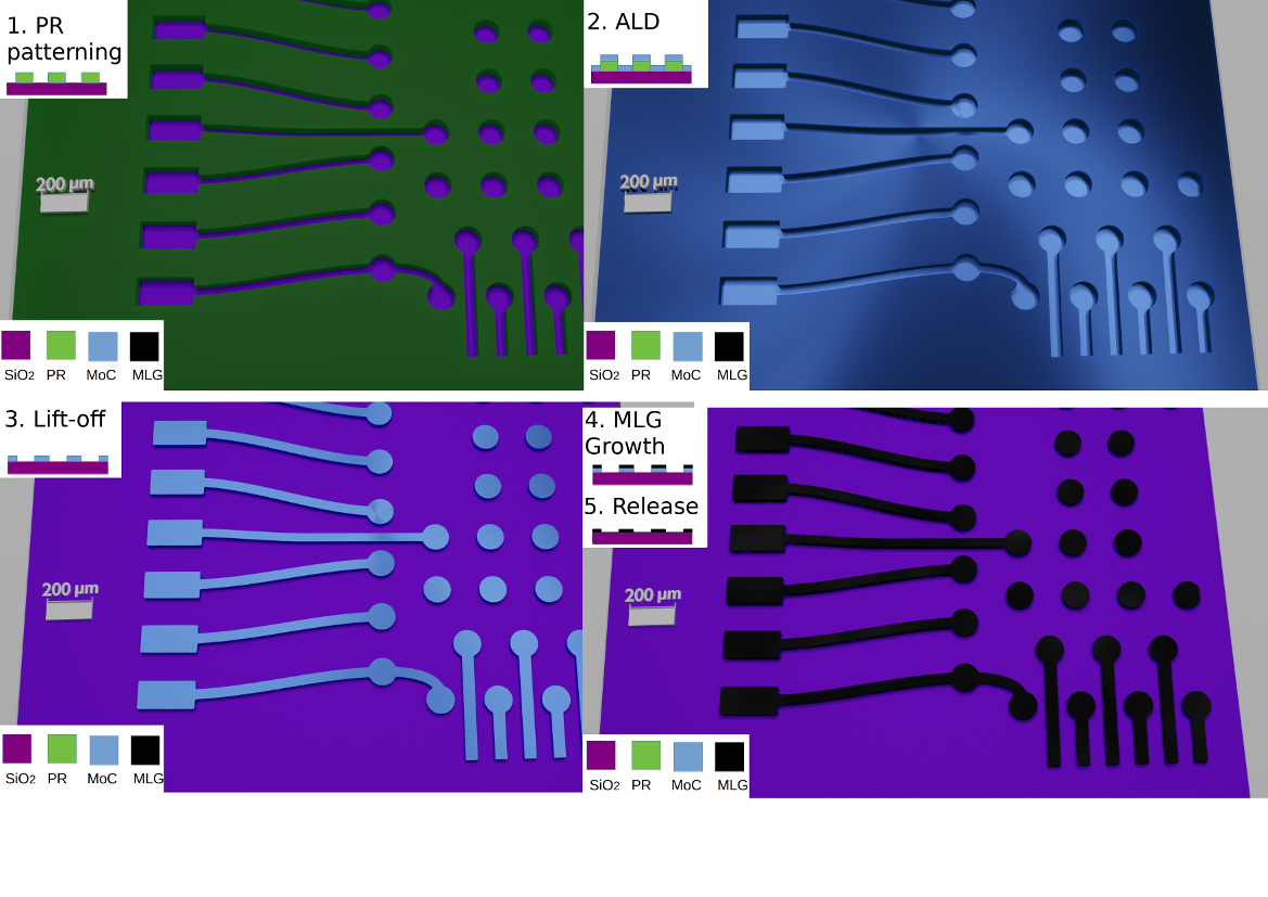
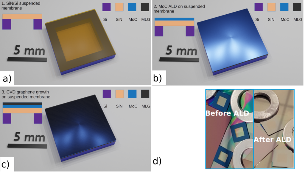
PEALD was performed on 100 mm Si (100) wafers coated with 450 nm of thermally grown . The depositions were performed in an Oxford instruments FlexAL2 ALD reactor, which is equipped with an inductively coupled remote RF plasma (ICP) source (13.56 MHz) with alumina dielectric tube. thin films have been deposited by PEALD at various temperatures and plasma conditions, with films varying from 15 to 30 in thickness. MLG was grown by low-pressure CVD (LPCVD) in a quartz tube (d=50mm, l=60cm) furnace with 3 heat zones set to 1050∘C. The typical base pressure when evacuated is mbar. The furnace is set on cart wheels, to allow samples to be rapid annealed, as furnace temperature stabilises within 3.5 minutes after tube insertion. When moved away from the furnace, sample cooling down duration is typically 15 minutes. Carbon feedstock gas () is fed along with Argon through a quartz inner tube of 5 mm in diameter to the sealed side of the outer tube. films have been saturated with carbon by annealing at temperatures between 500 to 800 with 100 sccm gas flow at 4 mbar pressure. Then, graphene films have been grown under similar conditions at 1100∘C for 10 minutes. The samples were then promptly extracted from the furnace and allowed to cool down at ambient room temperature under Ar gas flow in the quartz tube. As shown in figure 3(a) photoresist (PR) ma-N 400 with 4.1 thickness on 90 nm on Si 2” wafers were used for low temperature PEALD of film. After deposition, was patterned by lift-off process, and rinsed in isopropyl alcohol (IPA). 100 nm and 50 nm SiN membranes were supplied by Philips Innovation Services (PInS) foundry. were also deposited at 300 on 100 nm SiN membranes suspended on Si (5x5 mm suspended rectangular area). MLG were then grown the films as illustrated in figure 5. While deposition was successful for both SiN sample thicknesses, due to the brittle nature of the thinner membranes we present here results measured on the thicker 100nm based membranes. Raman spectroscopy was performed with Reinshaw InVia 514 nm laser. Film crystallinity and preferred crystal orientation was studied by Gonio x-ray diffraction. Experiments were conducted with PanAnlytical X’pert PROMRD diffractometer operated using .
3 Characterisation and Results
This section is divided to three parts: first part deals with MLG growth mechanism in films and comparison between amorphous and crystalline catalytic substrate. The second part demonstrate a technique for resist and transfer free patterned graphene device. In the third part we fabricate MLG on a thin suspended membrane using ALD and CVD. We show the limitation of Raman measurements on suspended membranes low thermal conductivity.
3.1 Carburisation of
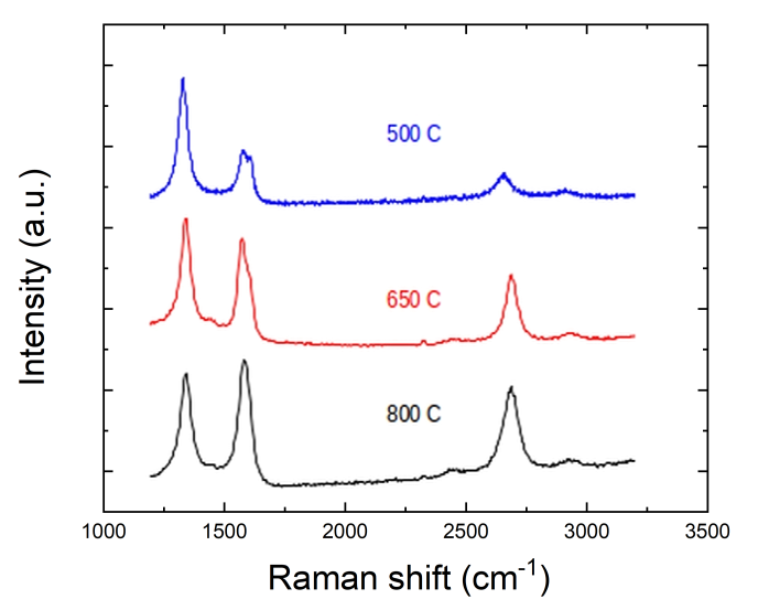
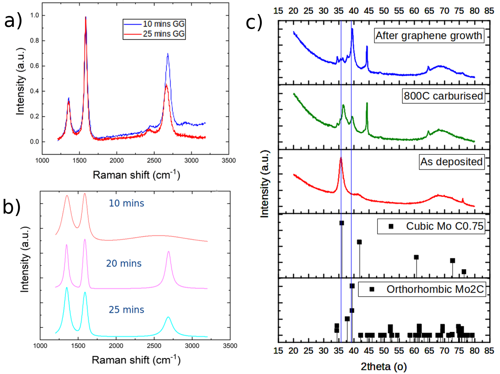
We studied the growth mechanism of graphene on substrates, to optimise growth process for the various film compositions. The importance of saturating the catalytic with free carbon is demonstrated and the effects of film crystallinity on carbon precipitation to the surface during growth is shown by Raman and XRD measurements. The mechanism of graphene growth on films is explained in this section. When we subjected the film to direct growth at 1100 for 10 minutes. SEM images show ablation on the film surface, that has a characteristic graphene Raman signature [1(a)]. Outside these areas, no indication of graphene growth was measured. We added then a carburisation step in order to saturate the film with carbon and examined different temperatures around the crystalline phase change temperature (). Figure 1(c) indicates that for crystalline film, ideal saturation takes place above the crystalline phase change, for MLG grown at the same growth time. The lack of sufficient carburisation affects the graphene growth significantly, as can be seen in figure 1(c). This effect is less dominant with amorphous, low mass density films, which can be carburised at lower temperatures as well. After establishing an optimal carburisation temperature, we examined the ideal growth time for various types. As seen in figure 2, with rich carbon content, typically low mass density and crystallinity exhibit good quality MLG growth after 10 minutes at 1100. films with higher mass density and crystallinity display no graphene growth at this time duration, but rather require a longer exposure time to at the growth temperature of 20 minutes. Longer exposure begin to deteriorate the graphene film. We study the physical alteration for this crystalline film during the carburisation and graphene growth process, as seen in figure 2. XRD diffraction peak typical to cubic- are dominant for the deposited film. After 2 hours carburisation at 800, a transition Orthorhombic crystalline phase is noted, along with sharp graphite (101) plane diffraction peak. After 10 minutes graphene growth at 1100, the orthorhombic phase crystallinity increases, while no significant change in the graphitic peak is noticed.
3.2 Patterned MLG Growth
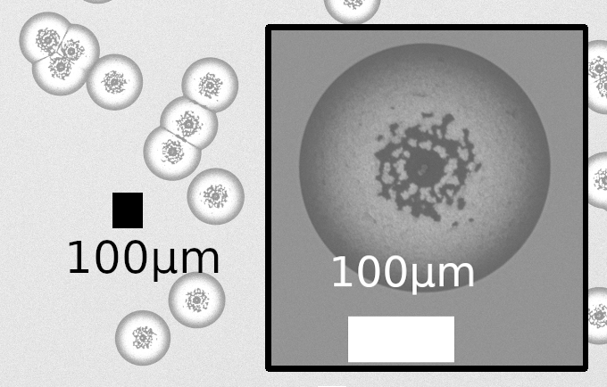
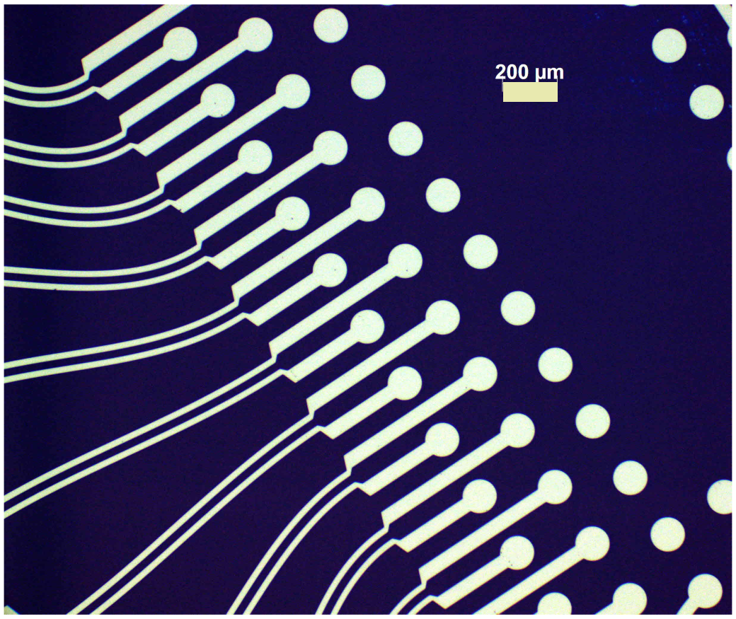
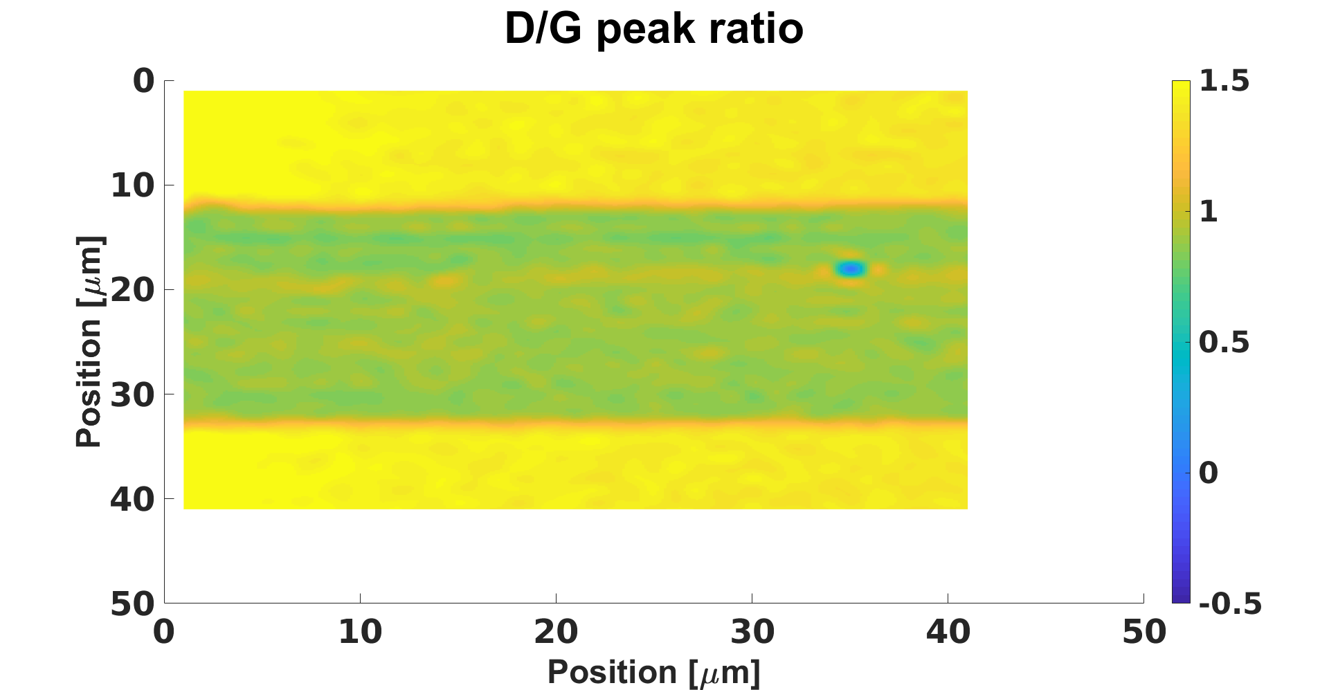
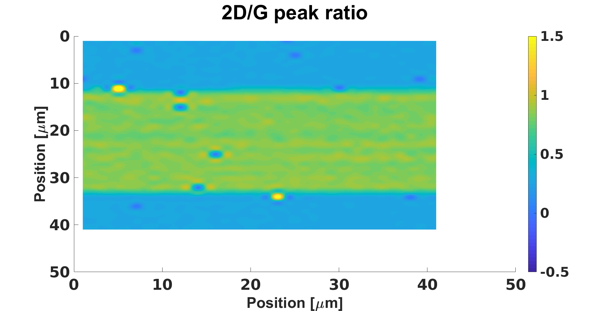
Graphene film has been grown on patterned catalytic substrates. Patterning of has been performed by a lift-off process, so that no exposed surface needed to be coated with PR. When depositing at 150 we found resist residues on the , due to hard baking of the photoresist at this temperature, as the thermal stability limits of the PR (110). Moreover, after the CVD growth we found random patches of MLG coverage on the exposed , and no continuous MLG coverage. However, when the PEALD is performed at 50, we could seamlessly remove the PR and no significant traces were found after lift-off. The CVD growth of graphene on these samples showed full MLG coverage with excellent uniformity, albeit a relatively high D/G peak ratio. Moreover, as can be seen in figure 4(a), D and G peaks were detected throughout the exposed areas, but no significant 2D peak. We have seen that a transfer free release of MLG on membranes is a direct result of wet etching the Mo based catalyst. This observation is valid for ultra thin layers with thicknesses below 30 nm. Thicker layers () release the MLG film such that the graphene membrane is afloat on the liquid surface.
3.3 MLG Growth on Suspended Thin Film
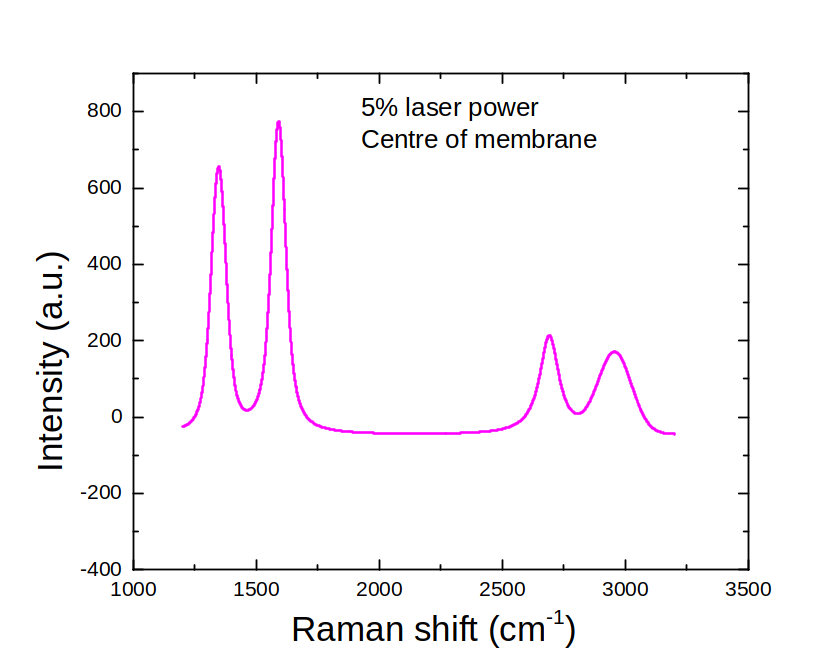
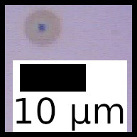
SiN membranes were suspended on Si substrate with 5x5 mm openings. was then deposited by PEALD process. There after, MLG was grown by a CVD growth process. Thus, a suspended heterostructure of MLG//SiN was fabricated on the supporting Si frame. MLG film grown on SiN membrane were characterised by Raman spectroscopy, as can be seen in 6. We measured the Raman signal at the edge of the suspended membrane where the SiN was supported by the underlying Si, and at the centre of the membrane, where the MLG was on top of nm and 100 nm SiN. The Raman spectrum was fitted and baseline corrected due to enhanced SiN background signal. Although Raman spectroscopy is considered a non-destructive measurement, we discovered that suspended MLG/SiN membranes were highly sensitive to the Raman laser power. As figure 6(c) shows, when 10% power of the 20mW Laser was used, an increase in the D peak was measured, and the 2D peak was quenched in comparison to 5% power. With 50% power of the Raman’s laser, we could punch a hole through the heterostructure suspended membrane as seen with an optical microscopy image [see figure 6(d) ].
4 Discussion and Conclusions
We have demonstrated in this work the growth mechanism and conditions of MLG on PEALD films. In order to achieve full graphene film coverage, and a uniform graphene growth, carburisation of the substrate is essential. The carburisation step allows for saturation of the catalytic film with free carbon. The free carbon then precipitate to the surface during annealing at 1100∘C. We found that in order to saturate film with higher mass density, carburisation temperature has to exceed the crystalline phase change point. For film we found that point to be around . Amorphous films with lower mass density could be saturated at lower carburisation temperatures.
We compared MLG growth time on amorphous film and on a highly crystalline one. The prolonged annealing time necessary to grow graphene on crystalline film is stipulated to result from low carbon saturation during carburisation, due to the dense crystal structure and the resulting low bulk precipitation of free carbon. Defects ratio of MLG on crystalline film could be explained with the transition from a single crystalline cubic- to a polycrystalline orthorhombic phase, which results in multiple strain points in the MLG film. By contrast, graphene growth on an amorphous carbon rich film is more facile and results in a lower D/G peak ratios.
After understanding the growth mechanism, we demonstrated the advantages of graphene growth on PEALD catalytic films. The low temperature, soft and atomic precise deposition allows for pre patterning of catalytic substrates, such that no PR coating of the growth surface is needed. We demonstrated here an initial proof of concept, which showed a full film coverage with excellent uniformity. We speculate that decomposition of the molecules on the surface with PR residue is the reason for the carbide formation outside the patterned areas. The relatively high D/G peak could be addressed by growth process optimisation, and different approaches to selective ALD which was out of the scope of this work. We cannot rule out potential surface impurities during the lift-off process, that could result in additional amorphous carbon during the CVD growth process. A complete bottom up selective area ALD process will avoid any potential resist contamination and should allow for a broader deposition window.
We have also used ALD to deposit films on brittle SiN membranes of 50 and 100 nm. The MLG growth demonstrated on 100 nm suspended membrane shows a viable fabrication route for sensor applications, and graphene based resonators for a wide range of frequencies. We showed for the first time damage to a suspended heterostructure caused directly by Raman measurements. The low thermal conductivity of the SiN is likely the cause for the local damage to the suspended heterostructure, with no directly available heat sink - as oppose to the membrane edges. This however could prove useful, when punctured suspended graphene heterostructures are required, for water filtration and desalination applications for example.
Building on the capabilities demonstrated here, the route for future application based on patterned graphene or suspended graphene heterostructure is clearly marked. Further steps, such as encapsulation, could be readily performed by ALD directly on the MLG without damage by a process of hydrogenation and post ALD annealing [19].
Moreover, one can combine recent developments in area selective ALD to realise a complete bottom up fabrication of the catalytic substrate resist free, with atomic-scale precision alignment.
Acknowledgements
This research is supported by the Dutch Technology Foundation STW (project number 140930), which is part of the Netherlands Organization for Scientific Research (NWO), and partly funded by the Ministry of Economic Affairs as well as ASML and ZEISS. E. Grady thanks Cristian Helvoirt, Janneke Zeegbregts, Jeroen van Gerwen and the lab technical staff for their support.
References
- [1] Veronica Strong, Sergey Dubin, Maher F El-Kady, Andrew Lech, Yue Wang, Bruce H Weiller, and Richard B Kaner. Patterning and electronic tuning of laser scribed graphene for flexible all-carbon devices. ACS nano, 6(2):1395–1403, 2012.
- [2] Rak-Hwan Kim, Myung-Ho Bae, Dae Gon Kim, Huanyu Cheng, Bong Hoon Kim, Dae-Hyeong Kim, Ming Li, Jian Wu, Frank Du, Hoon-Sik Kim, et al. Stretchable, transparent graphene interconnects for arrays of microscale inorganic light emitting diodes on rubber substrates. Nano letters, 11(9):3881–3886, 2011.
- [3] Ning C Wang, Saurabh Sinha, Brian Cline, Chris D English, Greg Yeric, and Eric Pop. Replacing copper interconnects with graphene at a 7-nm node. In 2017 IEEE International Interconnect Technology Conference (IITC), pages 1–3. IEEE, 2017.
- [4] Maria Politou, Xiangyu Wu, Inge Asselberghs, Antonino Contino, Bart Soree, Iuliana Radu, Cedric Huyghebaert, Zsolt Tokei, Stefan De Gendt, and Marc Heyns. Evaluation of multilayer graphene for advanced interconnects. Microelectronic Engineering, 167:1–5, 2017.
- [5] Yuji Awano. Graphene for vlsi: Fet and interconnect applications. In 2009 IEEE International Electron Devices Meeting (IEDM), pages 1–4. IEEE, 2009.
- [6] Shaloo Rakheja, Vachan Kumar, and Azad Naeemi. Evaluation of the potential performance of graphene nanoribbons as on-chip interconnects. Proceedings of the IEEE, 101(7):1740–1765, 2013.
- [7] Junmo Kang, Dolly Shin, Sukang Bae, and Byung Hee Hong. Graphene transfer: key for applications. Nanoscale, 4(18):5527–5537, 2012.
- [8] Woosuk Choi, Muhammad Arslan Shehzad, Sanghoon Park, and Yongho Seo. Influence of removing pmma residues on surface of cvd graphene using a contact-mode atomic force microscope. RSC Advances, 7(12):6943–6949, 2017.
- [9] Max C Lemme, David C Bell, James R Williams, Lewis A Stern, Britton WH Baugher, Pablo Jarillo-Herrero, and Charles M Marcus. Etching of graphene devices with a helium ion beam. ACS nano, 3(9):2674–2676, 2009.
- [10] Yong Seung Kim, Kisu Joo, Sahng-Kyoon Jerng, Jae Hong Lee, Euijoon Yoon, and Seung-Hyun Chun. Direct growth of patterned graphene on sio 2 substrates without the use of catalysts or lithography. Nanoscale, 6(17):10100–10105, 2014.
- [11] Mario Hofmann, Ya-Ping Hsieh, Allen L Hsu, and Jing Kong. Scalable, flexible and high resolution patterning of cvd graphene. Nanoscale, 6(1):289–292, 2014.
- [12] Keong Yong, Ali Ashraf, Pilgyu Kang, and SungWoo Nam. Rapid stencil mask fabrication enabled one-step polymer-free graphene patterning and direct transfer for flexible graphene devices. Scientific reports, 6:24890, 2016.
- [13] L Gustavo Cançado, A Jorio, EH Martins Ferreira, F Stavale, Carlos Alberto Achete, Rodrigo Barbosa Capaz, Marcus Vinicius de Oliveira Moutinho, Antonio Lombardo, TS Kulmala, and Andrea Carlo Ferrari. Quantifying defects in graphene via raman spectroscopy at different excitation energies. Nano letters, 11(8):3190–3196, 2011.
- [14] Nick FW Thissen, RHJ Vervuurt, JJL Mulders, JW Weber, WMM Kessels, and AA Bol. The effect of residual gas scattering on ga ion beam patterning of graphene. Applied Physics Letters, 107(21):213101, 2015.
- [15] Isaac Childres, Luis A Jauregui, Jifa Tian, and Yong P Chen. Effect of oxygen plasma etching on graphene studied using raman spectroscopy and electronic transport measurements. New Journal of Physics, 13(2):025008, 2011.
- [16] S Vollebregt, B Alfano, F Ricciardella, AJM Giesbers, Y Grachova, HW van Zeijl, T Polichetti, and PM Sarro. A transfer-free wafer-scale cvd graphene fabrication process for mems/nems sensors. In 2016 IEEE 29th International Conference on Micro Electro Mechanical Systems (MEMS), pages 17–20. IEEE, 2016.
- [17] Eldad Grady, Marcel Verheijen, Tahsin Faraz, Saurabh Karwal, W. M. M. Kessels, and Ageeth A. Bol. Tailored molybdenum carbide properties and graphitic nano layer formation by plasma and ion energy control during plasma enhanced ald, 2019.
- [18] Eldad Grady, W. M. M. Kessels, and Ageeth A. Bol. Control of graphene layer thickness grown on plasma enhanced atomic layer deposition of molybdenum carbide, 2019.
- [19] Rene HJ Vervuurt, Bora Karasulu, Marcel A Verheijen, Wilhelmus (Erwin) MM Kessels, and Ageeth A Bol. Uniform atomic layer deposition of al2o3 on graphene by reversible hydrogen plasma functionalization. Chemistry of Materials, 29(5):2090–2100, 2017.
Figures