The Apollo ATCA Platform
Abstract:
We have developed a novel and generic open-source platform - Apollo - which simplifies the design of custom Advanced Telecommunications Computing Architecture (ATCA) blades by factoring the design into generic infrastructure and application-specific parts. The Apollo ”Service Module” provides the required ATCA Intelligent Platform Management Controller, power entry and conditioning, a powerful system-on-module (SoM) computer, and flexible clock and communications infrastructure. The Apollo ”Command Module” is customized for each application and typically includes two large field-programmable gate arrays, several hundred optical fiber interfaces operating at speeds up to 28 Gbps, memories, and other supporting infrastructure. The command and service module boards can be operated together or independently on the bench without need for an ATCA shelf.
1 Introduction
The development of high-performance Advanced Telecommunications Computing Architecture (ATCA) blades for high-energy physics applications has proven to be quite challenging [1, 2]. Many problems must be solved, including: delivery of adequate cooling for 400 W of power; high-performance communications interfaces for control, monitoring and data acquisition; optical fiber management; and industry-standard debug and programming interfaces for routine monitoring and recovery of ”bricked” modules. The Apollo platform provides a relatively simple hardware environment and firmware and software toolkit which may be used to develop ATCA blades without reinventing all the required infrastructure.
We have constructed and tested 10 demonstrator modules which are currently in operation at test stands at collaborator institutes and at CERN. We describe the design in detail, show some test results and plans for further development and deployment in various LHC experiments.
This paper describes a demonstrator of the Apollo board developed in 2018 and 2019 at Boston University and Cornell University.
2 Overview
The ATCA standard defines a front board with dimensions 8U x 280 mm x 6 HP equipped with a face plate, top and bottom handles, indicator LEDs and a set of rear-facing backplane connectors. The Apollo service module (SM) is an ATCA-compliant front board with a large (7U x 180 mm) cutout in which a command module (CM) containing application-specific processing elements (see Fig. 1). The top surfaces of the SM and CM PCBs are co-planar but the PCBs need not be of identical thickness. A minimum of 2 board-to-board connectors provide electrical and mechanical connectivity between CM and SM, and the boards are securely joined by metal splice plates.
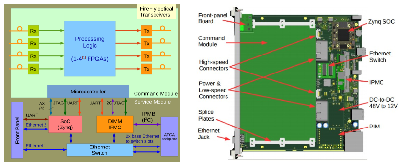
A block diagram is shown in Fig. 1. The SM contains power, communications and control infrastructure, providing , UART, JTAG and AXI chip-to-chip links to the CM. The CM can accommodate any hardware required for a particular application but the demonstrator contains two FPGAs as required by a typical LHC trigger/readout board.
3 IPMC
For the Apollo demonstrator we use the CERN IPMC[3], which is based on a hardware and software core provided by Pigeon Point. The essential functions of the IPMC are: (1) to read a set of critical parameters (temperature, current, voltage) from on-board sensors and deliver them to the ATCA shelf manager and (2) to mange power-up and power-down of the blade.
We have customized the IPMC extensively to perform several functions not foreseen by the ATCA standard: Xilinx Virtual Cable server for JTAG access; command interpreter accessible via TCP for GPIO and debugging; serial-over-LAN access to console ports of System on Chip (SoC) and CM microcontroller; and a more sophisticated power-up and power-down sequence.
4 SoC and Ethernet
A Xilinx Zynq SoC provides for overall control, monitoring, run control, and local DAQ functions for the blade. The demonstrator contains an Enclustra Mercury ZX1 module with a XC7Z035/45, providing a dual-core ARM Cortex-A9 CPU, 1 GB DDR3 SDRAM and two Ethernet ports. A total of four high-speed links (up to 10 Gbps) are routed to the SM for AXI chip-to-chip use. In the production hardware, the SoC will be upgraded to one supporting at least 64-bit CPUs and 4 GB of RAM.
Ethernet access is provided to the IPMC and SoC. An unmanaged Ethernet switch (ESM[1]) has a total of 6 ports, of which 5 are used as follows: 2 for ATCA base Ethernet from the backplane; one for a front-panel RJ-45 jack; one for SoC access, and one for the IPMC. An additional RJ-45 jack provides access to a dedicated gigabit Ethernet port on the SoC.
5 Clocks
An overview of Apollo demonstrator clock distribution is shown in Fig. 2. The SM can receive LHC machine clocks over the backplane or synthesize them from crystal oscillators on-board. The LHC clock is used for optical links from the detector, driven by the CERN LpGBT ASIC[4], while fixed-frequency clocks are used for Ethernet, AXI and 25 Gbps class optical links.
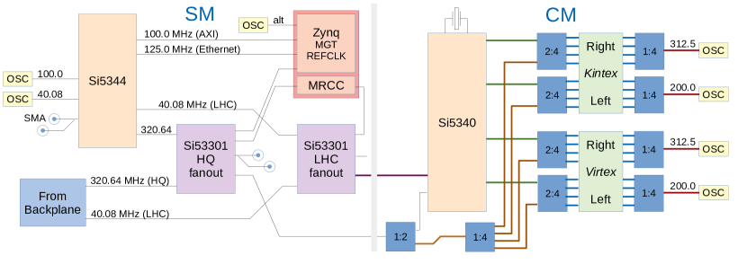
On the CM, clocks provided by the SM are distributed to a set of FPGA reference clock inputs, while an additional set of inputs is driven by local oscillators for bench testing.
6 Application-Specific Processing
The Apollo command-module is intended to be customized for each application, but they share many common features such as large FPGAs with ample logic resources and many high-speed fiber optic links. Three specific applications and their anticipated hardware needs are briefly presented.
The CMS Pixel DAQ and Timing Card (DTC) receives data from up to 512 front-end ASICs which deliver data in a complex, compressed data format. The total data rate for one DTC can approach 300 Gbps. Triggers are received from the CMS central trigger and must be converted to tokens and transmitted to the front-end. The received compressed data stream must be parsed in real time to build events. A separate trigger stream is processed for CMS luminousity monitoring system. The DTC is currently foreseen to require two XCVU7P or similar Virtex Ultrascale+ class FPGAs, 72 optical links at 10 Gbps and 16 optical links at 25 Gbps. A total of 28 pixel DTCs are required for CMS.
The CMS track finder uses pattern-matching to identify coincidences between “tracklets” transmitted from the readout modules and then uses a Kalman filter to establish precise track parameters. This application requires a smaller number of links than the DTC but substantial FPGA resources. The track finder is expected to require one large or two smaller Virtex Ultrascale+ FPGAs and 60 optical links at 25 Gbps. A total of between 126 and 180 track finder blades are required for CMS.
The ATLAS Monitored Drift-Tube Trigger Processor (MDTTP) performs a function similar to the combined functions of the DTC and track finder for CMS, but for the muon drift-tubes in ATLAS. Drift-tube hit data are received on about 60 fiber optic links, and a sophisticated two-dimensional fit is used to identify track segments. The segments are then joined to form tracks, and the Zynq processor is used to calculate transverse momentum for the identified tracks. In addition, drift-tube hits are buffered and stored until a trigger is received after which they are built into an event and sent to the DAQ. The MDTTP is expected to require one large Kintex Ultrascale+ FPGA and one Zynq Ultrascale+ SoC, along with 72 optical links at 10 Gbps and 12 optical links at 25 Gbps. A total of 64 MDTTP blades are required for ATLAS.
7 Prototypes and Test Results
A series of 10 demonstrator boards (Fig. 3) have been constructed. Each consists of a service module and a command module, and can recieve two FPGAs, an XCKU15P in an A1760 package, and an XCVU7P in a B2104 package. A total of 88 FireFly channels rated for 28 Gbps and 36 FireFly channels rated for 14 Gbps are provided along with the flexible clocking and power architecture described earlier.
Apollo blades have been deployed in several shelves at CERN and collaborator institutes. Remote access including firmware reprogramming and remote reset/power cycle have been proven. Optical links have been tested extensively at 10 Gbps and 25 Gbps and shown to be error-free.
The detailed design of customized command modules for specific applications is underway.
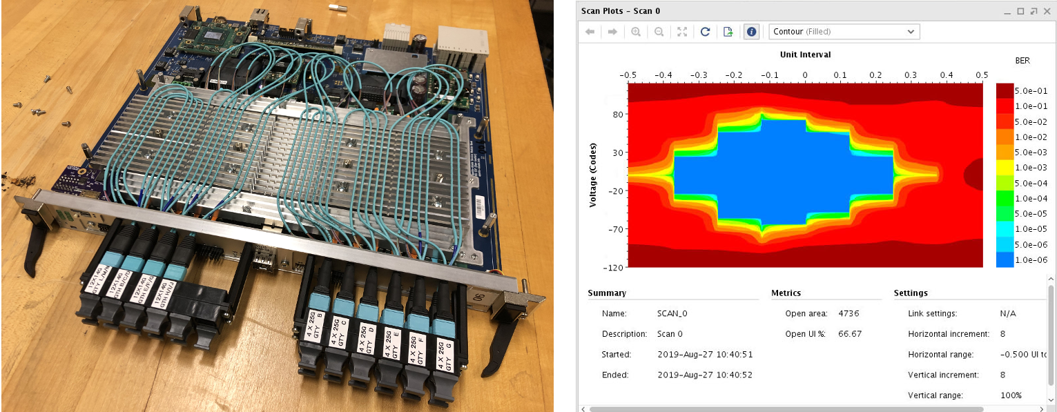
A CM developed at Cornell University has been mated with a SM developed at Boston University, as shown in Fig. 3. One KU15P and one VU7P Ultrascale+ FPGAs are installed. Two large heat sinks cool the FPGAs while two smaller heat sinks cool the FireFly optical transceivers. Optical fiber bundles are pressed into grooves machined in the heat sinks.
Figure 3 (right) shows an eye pattern for a fiber optic link test with loop-back fiber between two different quads on the XCVU9P FPGA. The horizontal axis is in fraction of one bit period (40 ps) and the vertical axis is arbitrary amplitude units. This represents a good result as logic “0” and logic “1” levels are well resolved in the middle of the bit period. Many combinations of links have been operated for hours with no bit errors seen.
8 Summary
We have developed a novel Apollo ATCA blade, designed for a wide range of applications. It is foreseen to be used in the CMS Pixel readout, the CMS track trigger, and the ATLAS drift-tube trigger processor.
References
-
[1]
W. Smith,
Next Generation ATCA Control Infrastructure for the CMS
Phase-2 Upgrades,
in TWEPP 2017, \posPoS(TWEPP-17)102 -
[2]
A. Rose,
Serenity - An ATCA prototyping platform for CMS Phase-2,
in TWEPP 2018, \posPoS(TWEPP-18)115 -
[3]
J. Mendez,
CERN-IPMC Solution for AdvancedTCA Blades,
in TWEPP 2018, \posPoS(TWEPP2018)059 - [4] P. Moreira, The lpGBT: a radiation tolerant ASIC for Data, Timing, Trigger and Control Applications in HL-LHC, in TWEPP 2019, \posPoS(TWEPP2019)