Enhanced shot noise at bilayer graphene - superconductor junction
Abstract
Transport properties of graphene - superconductor junction has been studied extensively to understand the interplay of the relativistic Dirac quasiparticles and superconductivity. Though shot noise measurements in graphene has been performed to realize many theoretical predictions, both at zero magnetic field as well as quantum Hall (QH) regime, its junction with superconductor remain unexplored. Here, we have carried out the shot noise measurements in an edge contacted bilayer graphene - Niobium superconductor junction at zero magnetic field as well as QH regime. At the Dirac point we have observed a Fano factor above the superconducting gap () and a transition to an enhanced Fano factor below the superconducting gap. By changing the carrier density we have found a continuous reduction of Fano factor for both types of carriers, however the enhancement of Fano factor within the superconducting gap by a factor of is always preserved. The enhancement of shot noise is also observed in the QH regime, where the current is carried by the edge state, below the critical magnetic field and within the superconducting gap. These observations clearly demonstrate the enhanced charge transport at the graphene-superconductor interface.
I INTRODUCTION
Engineering a topological superconductor, which can host exotic non-abelian Majorana quasi-particlesFu and Kane (2008), has been one of the emerging research areas in mesoscopic condensed matter physicsLutchyn et al. (2010); Oreg et al. (2010); Mourik et al. (2012); Das et al. (2012a); Mong et al. (2014); Clarke et al. (2014). Realizing superconducting correlations in a quantum Hall edge has been proposed as a novel route for creating even more exotic topological entities, such as parafermionOrth et al. (2015) or Fibbonacci particlesMong et al. (2014). The conventional conductance measurement is the well developed technique to probe the superconducting correlations. However, in many cases various important information stay hidden in this technique due to its averaging nature. In such cases shot noise measurement has been proven to be an unique tool for studying physics of different kind of interactionsKhlus (1987); De Jong and Beenakker (1996); Blanter and Büttiker (2000); Kaviraj et al. (2011); Hata et al. (2018); Oberholzer et al. (2002); Choi et al. (2005); Ota et al. (2017); Beenakker et al. (2003); Das et al. (2012b); Steinbach et al. (1996); Lefloch et al. (2003), such as the effective charge () of the quasiparticle. Observing enhanced charge transport () at QH - superconductor junction would be a first step in realizing superconducting correlations in the QH edge.
In the last two decades shot noise technique has been extensively used either to understand or to produce many interesting physics, such as one third Fano factor in disordered metalBeenakker and Büttiker (1992); Nagaev (1992); Steinbach et al. (1996); Henny et al. (1999), fractional charge in Fractional QH regimeSaminadayar et al. (1997); Reznikov et al. (1999); Hashisaka et al. (2015), charge doubling in normal metal-superconductor (NS) junctionDe Jong and Beenakker (1994); Jehl et al. (2000); Nagaev and Büttiker (2001), discrete quantization of charge in multiple Andreev reflection (AR)Ronen et al. (2016); Hoss et al. (2000). In graphene one third Fano factor has been obseved at the Dirac point Tworzydło et al. (2006); DiCarlo et al. (2008); Danneau et al. (2008). Further shot noise measurement is performed in graphene PN junctions at zero magnetic field as well as in the QH regimeKumada et al. (2015); Matsuo et al. (2015); Abanin and Levitov (2007). However, the shot noise at graphene - superconductor junction is not studied till date to understand the effect of Andreev processes in these hybrids both at zero magnetic field and QH regime.

In this work we have carried out the shot noise measurement in a bilayer graphene (BLG) - Niobium (Nb) superconductor junction. We have observed the Fano factor at the Dirac point for normal quasi-particle transport above the superconducting gap (). Whereas within the superconducting gap (), when the transport occurs via AR, an enhanced Fano factor is observed. The schematic of the Andreev processSahu et al. (2016); Soori et al. (2018); Shalom et al. (2016); Lee and Lee (2018) is shown in Fig. 1a-left panel. By increasing the carrier density we found a continuous reduction of Fano factor for both normal transport as well as Andreev process signifying the quasi-ballistic nature of the device. However, the enhancement of Fano factor by a factor of due to the Andreev process compared to normal transport was observed at all carrier densities. The AR in the QH regimeRickhaus et al. (2012); Shalom et al. (2016); Amet et al. (2016); Lee et al. (2017); Park et al. (2017); Sahu et al. (2018); Lee and Lee (2018) is shown schematically in Fig. 1a-right panel, where the shot noise is being created due to the finite barrier at the interface between the edge state and the superconductor. An enhanced shot noise is also observed at the QH-superconductor junction within the superconducting gap () and below the critical magnetic field of the Nb superconductor. The enhancement of shot noise at the graphene-superconductor junction clearly suggests the enhanced charge transport () in our experiment.
II DEVICE FABRICATION AND CHARACTERIZATION
The device consists of an edge contacted Bilayer graphene connected to a Gold (Au) contact at one end and a Niobium superconducting contact at other end. The device was fabricated using standard dry transfer techniquePizzocchero et al. (2016). The normal contact was achieved by electron beam lithography followed by dry ion etching and thermal deposition of Cr/Pd/Au (3/9/68 nm). The superconducting contact was achieved using the same technique and by deposition of Ti/Nb (5/30 nm) using sputtering. The channel length (L) and width (W) of device are and , respectively, which makes W/L 3 (Fig. 1(b) inset).
All the measurements were done in a cryofree dilution refrigerator having base temperature of . The conductance measurement was done using standard lock-in technique at 728 Hz in two probe configuration and we have subtracted the line resistances for all the presented data. The shot noise measurements were performed using LCR resonant circuit at 710 kHz. The gate response of the device is shown in the Fig. 1(b), from which we have extracted the contact resistance 700-800 (Supplementary Fig. 2) of the device. The measured contact resistance is comparatively higher than the typical contact resistance values for graphene devices with Cr/Pd/Au contacts at both sides. The higher contact resistance is possibly due to the Ti/Nb contact. The superconducting gap and the critical magnetic field () of thick Nb film was characterized separately as shown in Supplementary Fig. 1. The was found to be 4T and from the critical temperature (7 K) of the film we found (=3.528). Note that the 30 nm thin Nb film was chosen in order to have higher .
III Experimental setup
Fig. 1(c) shows the schematic of the shot noise measurement setup . The voltage fluctuations were measured using LCR resonant circuit tuned to 710 kHz (Supplementary Fig. 3), amplified by a home made preamplifier at 4K plate followed by a room temperature amplifier and finally measured by a spectrum analyzer. The total gain (g 1300) of the system was measured using a known signal as well as by measuring the thermal noise in the QH regime of graphene. Details of gain calibration is shown in Supplementary Fig. 4.
The measured total noise contains various other noises together with the desired shot noise component (, which is the current dependent excess noise), given byRonen et al. (2016); Srivastav et al. (2019)
| (1) |
where is the parallel resistance of the sample () and the load resistor (), is the thermal noise, and are the current and voltage noise of the cold amplifier (CA), respectively. Thus, the shot noise (excess noise) can be extracted from the total noise as, .
IV Shot noise measurement at zero magnetic field
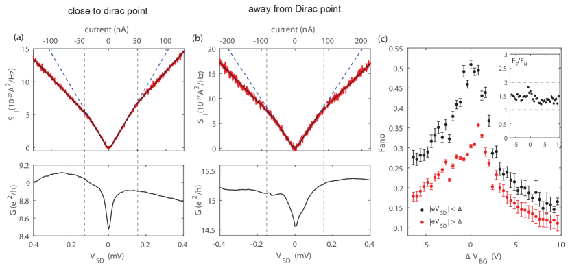
Shot noise measured at B=0 is shown in Fig. 2 revealing many interesting features. Fig. 2(a) (top) shows the shot noise as a function of applied DC current close to the Dirac point () which shows two distinct slopes, one at lower current () and other at relatively larger current (). The outer slope is due to normal quasi-particle transport where as the inner higher slope corresponds to transport by AR. The bias () dependence of differential conductance () at the same gate voltage is shown in Fig. 2(a) (bottom) showing BCS like features with a proximity induced gap of 2. To extract out the Fano factor, which is the measured shot noise normalized by Poisson noise (2eI), for both normal transport () as well as transport via AR (), we have fitted the noise data with the following equations,
| (2) |
where is the electronic charge, e∗=2e, is the Boltzmann constant, is the electron temperature and is a constant. Fitting the shot noise data at the Dirac point (Fig. 2a) gives and , respectively. Using the shot noise data the electron temperature () 40 mK was evaluated as shown in Supplementary Fig. 5. The measured value at the Dirac point is close to the theoretically predicted valueTworzydło et al. (2006); Snyman and Beenakker (2007) as reported in single layer graphene DiCarlo et al. (2008); Danneau et al. (2008) and attributed to pseudo-diffusive transport by evanescent modes. Ideally, one would expect for an NS interface due to Cooper pair (2e) transport, however, we observe near the Dirac point. Similar deviation has been reported in topological insulator (TI) - Nb junctionTikhonov et al. (2016) and the reduction of Fano factor is attributed to the presence of residual density of states at the interface. Fig. 2(b) shows the shot noise spectrum along with corresponding bias spectrum away from the Dirac point (), where the fitting gives and . Fano factors for both and as a function of are shown in Fig. 2(c), which shows a continuous reduction of Fano factors away from the Dirac point indicating the quasi-ballistic nature of the deviceTworzydło et al. (2006); Snyman and Beenakker (2007). Inset shows ratio as a function of , where average enhancement of Fano factor by 1.5 can be clearly seen at all carrier densities.
V SHOT NOISE IN THE QH REGIME
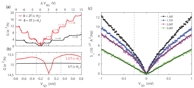
In order to measure the shot noise in QH regime we applied perpendicular magnetic field and the device starts showing clean quantum Hall plateaus at B as low as 1 T. Fig. 3(a) shows the quantum Hall plateaus at B = 2 T () and B = 5 T (), respectively. Fig. 3(b) shows the bias spectrums measured at the centers of plateau at and plateau at . The bias spectrum at 1.3T (< BC) shows BCS like features with proximity induced superconducting gap, 2, which is not present in the bias spectrum at 5T (> BC). The shot noise data at the center of plateau at several magnetic fields are shown in Fig. 3(c). For a QH edge with fully transparent contacts the shot noise is not expected due to the ballistic nature of the edge state. However, the presence of finite barrier at the interface of quantum Hall edge and the contact will reduce the transmission probability from unity and thus, can create shot noise. The shot noise at 5T with a single slope in Fig. 3(c) is expected for normal quasi-particle transport above the critical field.
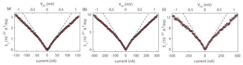
The generated shot noise can be quantified by extracting the Fano factors using equation 2. At 5T the 0.056 is extracted from the fitting in Fig. 3(c). Below the critical field, the slope at lower bias voltage () is larger compared to the slope at higher bias (()), similar to the zero magnetic field case. The enhancement of shot noise within the superconducting gap and below the critical magnetic field is the signature of Andreev conversions happening at the QH edge and superconductor interface. Moreover, it can be seen from Fig. 3c that the total noise decreases with increasing B (<), both for as well as for . The increment of Fano factors at lower magnetic field could be due to the bulk contribution to the net current, which is expected at lower magnetic field (), when the Landau level broadening ()Sahu et al. (2018) is comparable to the Landau level gap (). However, it can be seen from Fig. 5a that the Fano factors saturate beyond B=2 T, as the Landau level gap becomes higher with increasing magnetic field. This saturating behavior signifies that beyond B=2 T, the dominant shot noise contribution comes from the edge transport. Similar shot noise data at several other plateaus along with fitted curves using equation 2 is shown in Fig. 4, clearly showing an enhanced shot noise for due to Andreev reflections.
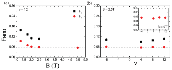
Fig. 5(a) shows the and plotted as a function of magnetic field for filling factor, where the saturating behavior of both the and is apparent. The and for different filling factors at B=2.5 T are shown in Fig. 5b, where both the Fano factors are pretty constant with an enhancement factor . The figure 5(b) inset shows the for different filling factors at B=5 T.
Currently, there is no well developed theory for shot noise at the interface of QH edge and a superconductor. Some insights can be gained by considering a ballistic system containing a finite number of modes connected to a superconductor. In such a system, when the superconductor is in normal state, a finite contact resistance can generate shot noise with Fano factor, FN=1-tN, where tN is the transmittance of the ballistic modes. When the lead becomes superconducting the transmittance and the Fano factor will take the formBlanter and Büttiker (2000) tS= t/(2-tN)2 and Choi et al. (2005) FS=8(1-tN)/(2-tN)2, respectively. The ratio of the Fano factors, FS/FN=8/(2-tN)2, will take the minimum value of 2 in the tunneling regime (tN tends to zero) whereas it will take the maximum value of 8 in the highly transparent regime (tN tends to one). This suggests that the enhancement of shot noise at the QH-superconductor junction is not universal. Moreover, a finite magnetic field can complicate the problem further due to the presence of inevitable vortices in the superconducting lead. The presence of votices can create pathways for normal quasiparticle transportMiyoshi et al. (2005) at the junction, and thus can reduce the ratio of Fano factors from the expected range of values of 2 to 8.
The measured enhancement of Fano factor by 2 times (Fig. 5) in our highly transparent junction (conductance data in Fig. 3a) is much lesser than the expected value of 8. More theoretical understanding is necessary to quantify the shot noise at the QH-superconductor junction considering the complex nature of dynamics (Fig. 1a - right panel) as well as the presence of vortices. Nevertheless, the enhancement of Fano factor by a factor of indicates the enhanced charge transport due to Andreev processes at the QH-superconductor junction, but it does not establish the doubling of charge (e∗=2e). We would like to note that there could be noise contribution coming from the normal-QH junction of the device (normal-QH-superconductor), however, that component will not produce a bias dependent slope, and thus will not affect the conclusion of observing enhanced charge transport in our experiment.
VI CONCLUSION
In conclusion, we have performed the shot noise measurement in a BLG - superconductor junction for the first time. Below the superconducting gap, when the current is carried via Andreev reflections, enhancement of Fano factor by times is observed irrespective of carrier densities. More importantly, we have also observed an enhanced shot noise by times in the QH regime below the superconducting gap and below the critical magnetic field. The enhancement of shot noise in our experiment clearly signifies the enhanced charge transport at BLG-superconductor junction. However, more theoretical studies are required to understand and quantify the shot noise due to Andreev processes at the quantum Hall - superconductor interface. We believe that our work will pave the way for more investigations utilizing shot noise measurement technique as a tool to study quantum Hall - superconductor hybrids.
VII ACKNOWLEDGMENTS
AD thanks DST Nanomission (DSTO2051) for financial support. AS thanks DST Nanomission (DSTO1597) for funding.
References
- Fu and Kane (2008) L. Fu and C. L. Kane, Physical review letters 100, 096407 (2008).
- Lutchyn et al. (2010) R. M. Lutchyn, J. D. Sau, and S. D. Sarma, Physical review letters 105, 077001 (2010).
- Oreg et al. (2010) Y. Oreg, G. Refael, and F. von Oppen, Physical review letters 105, 177002 (2010).
- Mourik et al. (2012) V. Mourik, K. Zuo, S. M. Frolov, S. Plissard, E. Bakkers, and L. Kouwenhoven, Science 336, 1003 (2012).
- Das et al. (2012a) A. Das, Y. Ronen, Y. Most, Y. Oreg, M. Heiblum, and H. Shtrikman, Nature Physics 8, 887 (2012a).
- Mong et al. (2014) R. S. Mong, D. J. Clarke, J. Alicea, N. H. Lindner, P. Fendley, C. Nayak, Y. Oreg, A. Stern, E. Berg, K. Shtengel, et al., Physical Review X 4, 011036 (2014).
- Clarke et al. (2014) D. J. Clarke, J. Alicea, and K. Shtengel, Nature Physics 10, 877 (2014).
- Orth et al. (2015) C. P. Orth, R. P. Tiwari, T. Meng, and T. L. Schmidt, Physical Review B 91, 081406 (2015).
- Khlus (1987) V. Khlus, Zh. Eksp. Teor. Fiz 93, 2179 (1987).
- De Jong and Beenakker (1996) M. De Jong and C. Beenakker, Physica A: Statistical Mechanics and its Applications 230, 219 (1996).
- Blanter and Büttiker (2000) Y. M. Blanter and M. Büttiker, Physics reports 336, 1 (2000).
- Kaviraj et al. (2011) B. Kaviraj, O. Coupiac, H. Courtois, and F. Lefloch, Physical review letters 107, 077005 (2011).
- Hata et al. (2018) T. Hata, R. Delagrange, T. Arakawa, S. Lee, R. Deblock, H. Bouchiat, K. Kobayashi, and M. Ferrier, Physical review letters 121, 247703 (2018).
- Oberholzer et al. (2002) S. Oberholzer, E. Sukhorukov, and C. Schönenberger, Nature 415, 765 (2002).
- Choi et al. (2005) B.-R. Choi, A. Hansen, T. Kontos, C. Hoffmann, S. Oberholzer, W. Belzig, C. Schönenberger, T. Akazaki, and H. Takayanagi, Physical Review B 72, 024501 (2005).
- Ota et al. (2017) T. Ota, M. Hashisaka, K. Muraki, and T. Fujisawa, Journal of Physics: Condensed Matter 29, 225302 (2017).
- Beenakker et al. (2003) C. Beenakker, C. Schönenberger, et al., Physics Today 56, 37 (2003).
- Das et al. (2012b) A. Das, Y. Ronen, M. Heiblum, D. Mahalu, A. V. Kretinin, and H. Shtrikman, Nature communications 3, 1165 (2012b).
- Steinbach et al. (1996) A. H. Steinbach, J. M. Martinis, and M. H. Devoret, Physical review letters 76, 3806 (1996).
- Lefloch et al. (2003) F. Lefloch, C. Hoffmann, M. Sanquer, and D. Quirion, Physical review letters 90, 067002 (2003).
- Beenakker and Büttiker (1992) C. Beenakker and M. Büttiker, Physical Review B 46, 1889 (1992).
- Nagaev (1992) K. Nagaev, Physics Letters A 169, 103 (1992).
- Henny et al. (1999) M. Henny, S. Oberholzer, C. Strunk, and C. Schönenberger, Physical Review B 59, 2871 (1999).
- Saminadayar et al. (1997) L. Saminadayar, D. Glattli, Y. Jin, and B. c.-m. Etienne, Physical Review Letters 79, 2526 (1997).
- Reznikov et al. (1999) M. Reznikov, R. De Picciotto, T. Griffiths, M. Heiblum, and V. Umansky, Nature 399, 238 (1999).
- Hashisaka et al. (2015) M. Hashisaka, T. Ota, K. Muraki, and T. Fujisawa, Physical review letters 114, 056802 (2015).
- De Jong and Beenakker (1994) M. De Jong and C. Beenakker, Physical Review B 49, 16070 (1994).
- Jehl et al. (2000) X. Jehl, M. Sanquer, R. Calemczuk, and D. Mailly, Nature 405, 50 (2000).
- Nagaev and Büttiker (2001) K. Nagaev and M. Büttiker, Physical Review B 63, 081301 (2001).
- Ronen et al. (2016) Y. Ronen, Y. Cohen, J.-H. Kang, A. Haim, M.-T. Rieder, M. Heiblum, D. Mahalu, and H. Shtrikman, Proceedings of the National Academy of Sciences 113, 1743 (2016).
- Hoss et al. (2000) T. Hoss, C. Strunk, T. Nussbaumer, R. Huber, U. Staufer, and C. Schönenberger, Physical Review B 62, 4079 (2000).
- Tworzydło et al. (2006) J. Tworzydło, B. Trauzettel, M. Titov, A. Rycerz, and C. W. Beenakker, Physical Review Letters 96, 246802 (2006).
- DiCarlo et al. (2008) L. DiCarlo, J. Williams, Y. Zhang, D. McClure, and C. Marcus, Physical review letters 100, 156801 (2008).
- Danneau et al. (2008) R. Danneau, F. Wu, M. Craciun, S. Russo, M. Tomi, J. Salmilehto, A. Morpurgo, and P. J. Hakonen, Physical review letters 100, 196802 (2008).
- Kumada et al. (2015) N. Kumada, F. Parmentier, H. Hibino, D. Glattli, and P. Roulleau, Nature communications 6, 8068 (2015).
- Matsuo et al. (2015) S. Matsuo, S. Takeshita, T. Tanaka, S. Nakaharai, K. Tsukagoshi, T. Moriyama, T. Ono, and K. Kobayashi, Nature communications 6, 8066 (2015).
- Abanin and Levitov (2007) D. Abanin and L. Levitov, Science 317, 641 (2007).
- Sahu et al. (2016) M. R. Sahu, P. Raychaudhuri, and A. Das, Physical Review B 94, 235451 (2016).
- Soori et al. (2018) A. Soori, M. R. Sahu, A. Das, and S. Mukerjee, Physical Review B 98, 075301 (2018).
- Shalom et al. (2016) M. B. Shalom, M. Zhu, V. FalKo, A. Mishchenko, A. Kretinin, K. Novoselov, C. Woods, K. Watanabe, T. Taniguchi, A. Geim, et al., Nature Physics 12, 318 (2016).
- Lee and Lee (2018) G.-H. Lee and H.-J. Lee, Reports on Progress in Physics 81, 056502 (2018).
- Rickhaus et al. (2012) P. Rickhaus, M. Weiss, L. Marot, and C. Schonenberger, Nano letters 12, 1942 (2012).
- Amet et al. (2016) F. Amet, C. T. Ke, I. V. Borzenets, J. Wang, K. Watanabe, T. Taniguchi, R. S. Deacon, M. Yamamoto, Y. Bomze, S. Tarucha, et al., Science 352, 966 (2016).
- Lee et al. (2017) G.-H. Lee, K.-F. Huang, D. K. Efetov, D. S. Wei, S. Hart, T. Taniguchi, K. Watanabe, A. Yacoby, and P. Kim, Nature Physics 13, 693 (2017).
- Park et al. (2017) G.-H. Park, M. Kim, K. Watanabe, T. Taniguchi, and H.-J. Lee, Scientific reports 7, 10953 (2017).
- Sahu et al. (2018) M. R. Sahu, X. Liu, A. K. Paul, S. Das, P. Raychaudhuri, J. K. Jain, and A. Das, Physical review letters 121, 086809 (2018).
- Pizzocchero et al. (2016) F. Pizzocchero, L. Gammelgaard, B. S. Jessen, J. M. Caridad, L. Wang, J. Hone, P. Bøggild, and T. J. Booth, Nature communications 7, 11894 (2016).
- Srivastav et al. (2019) S. K. Srivastav, M. R. Sahu, K. Watanabe, T. Taniguchi, S. Banerjee, and A. Das, Science Advances 5 (2019).
- Snyman and Beenakker (2007) I. Snyman and C. Beenakker, Physical Review B 75, 045322 (2007).
- Tikhonov et al. (2016) E. Tikhonov, D. Shovkun, M. Snelder, M. Stehno, Y. Huang, M. Golden, A. A. Golubov, A. Brinkman, and V. Khrapai, Physical review letters 117, 147001 (2016).
- Miyoshi et al. (2005) Y. Miyoshi, Y. Bugoslavsky, and L. Cohen, Physical Review B 72, 012502 (2005).
See pages - of hh.pdf