Unveiling the Semimetallic Nature of 1-TiSe2 by Doping its Charge Density Wave
Abstract
The semimetallic or semiconducting nature of the transition metal dichalcogenide 1-TiSe2 remains under debate after many decades mainly due to the fluctuating nature of its 2 2 2 charge-density-wave (CDW) phase at room-temperature. In this letter, using angle-resolved photoemission spectroscopy, we unambiguously demonstrate that the 1-TiSe2 normal state is semimetallic with an electron-hole band overlap of 110 meV by probing the low-energy electronic states of the perturbed CDW phase strongly doped by alkali atoms. Our study not only closes a long-standing debate but also supports the central role of the Fermi surface for driving the CDW and superconducting instabilities in 1-TiSe2.
Layered transition-metal dichalcogenides (TMDCs) have attracted considerable interest due to their rich phase diagrams including intertwined charge-density-waves (CDWs), Mott states and superconductivity Morosan et al. (2006); Sipos et al. (2008); Kusmartseva et al. (2009). A common feature that explains the intrinsic tendency of these materials to exhibit electronic phase transitions is that their density of states close to the Fermi level (), dominated by the -orbitals of the transition metal layers, is usually high Novoselov et al. (2016); Wilson and Yoffe (1969). Although 1-TiSe2 is a prototypical material with a 2 2 2 commensurate CDW occuring at 200 K and hosting superconductivity under pressure, Cu-doping or electrical gating Kusmartseva et al. (2009); Morosan et al. (2006); Li et al. (2015), its normal state still remains elusive after many decades, due to the fluctuating nature of the CDW at room-temperature (RT) Jaouen et al. (2019). Whereas transport measurements Di Salvo et al. (1976); Wilson et al. (1978) as well as recent optical spectroscopy and conductivity studies Li et al. (2007); Velebit et al. (2016), all concluded on a semimetallic normal state with electron-hole () band overlap -100 meV, three-dimensional (3D) momentum-resolved angle-resolved photoemission spectroscopy (ARPES) measurements have reported RT values of band gaps up to 150 meV Rossnagel et al. (2002); Kidd et al. (2002); Zhao et al. (2007); Rasch et al. (2008); Chen et al. (2016); Watson et al. (2019).

The key point is that the bare electronic band structure of the 1-TiSe2 non-distorted phase is not accessible to RT ARPES measurements due to the presence of strong short-range fluctuations. The result is that ARPES probes a ”pseudogap” CDW state as manifested by the presence of diffuse backfolded band intensities and suppression of spectral weight Jaouen et al. (2019); Monney et al. (2015, 2012a); Borisenko et al. (2008); Pillo et al. (1999). In this letter, we show that the normal-state band structure of 1-TiSe2 can be revealed from the low-temperature (LT) CDW state strongly doped by alkali atoms. This therefore closes a long-standing debate by demonstrating that 1-TiSe2 is a semimetal with an band overlap of 110 meV.
In the 1 1 1 normal state, the 1-TiSe2 low-energy electronic states consist of a Se 4 hole pocket (labeled ) at and Ti 3 electron pockets (labeled , , and ) at the three equivalent points of the 3D Brillouin zone (BZ) [see Fig. 1 (a)-(b)]. At the CDW transition, i.e. with a non-zero order parameter , the and the points are connected by the three new reciprocal lattice -vectors leading to the doubling of the lattice periodicity [Fig. 1(c)]. As a result, becomes equivalent to and the electron pockets at , backfolded to produce ”flowerlike” Fermi surfaces (FSs) at each newly equivalent high-symmetry point Monney et al. (2012b).
The most recent proposals for the electron and hole band configurations in the normal state Jaouen et al. (2019); Watson et al. (2019), are an initial semimetallic band overlap of 110 meV Jaouen et al. (2019) [Fig. 1 (d), left panel] or a semiconducting band gap of 74 meV Watson et al. (2019) [Fig. 1 (e), left panel]. The corresponding calculated band dispersions and spectral functions of the CDW state 111Details on the model from which the near- dispersions and spectral functions describing ARPES have been computed can be found in Refs. Monney et al. (2009); Jaouen et al. (2019). [Fig. 1 (d)-(e), middle panels] for both cases are very similar, despite having different values of (118 and 45 meV for the semimetal and the semiconductor, respectively) calculated for obtaining identical values of the binding energy (BE) of the backfolded band 222In a photoemission experiment, we can extract the order parameter from the shift of the backfolded valence band, using, (1) where is the band overlap ( 0) or band gap ( 0) in the normal state.Jaouen et al. (2019). Indeed, compared with both of the normal state band configurations, in the CDW state the valence band [orange band] and the conduction band [green band] repel each other symmetrically around . The and bands remain at their original positions and in addition the band [blue band, middle panels] has no spectral weight Monney et al. (2009). Therefore, the normal state of 1-TiSe2 can not be extrapolated from photoemission measurements of the CDW state.
However, upon sufficient electron-doping which induces a chemical-potential shift () and a reduction of , clear differences between the LT band structures of an initial semimetallic and semiconducting band configurations now appear [Fig. 1(d)-(e), right panels]. In particular, the ”smoking gun” spectral fingerprints in ARPES for a semimetallic normal-state are: the so-called ”Mexican hat” shape of [black vertical arrow on the right panel of Fig. 1(d)] associated with the top of the CDW-split hole band shifted below ; gaps at the avoided crossings of the electron and hole bands [black horizontal arrows on the right panel of Fig. 1(d)]; as well as the shift of the backfolded band () towards . For that purpose, here we electron-dope the CDW state of 1-TiSe2 using LT depositions of potassium (K) atoms in order both to access the unoccupied part of the band structure and to lower which is known to be highly sensitive to doping Qian et al. (2007); Jaouen et al. (2019); Hildebrand et al. (2017); Li et al. (2015).
The 1-TiSe2 single crystals were grown by chemical vapor transport at 590 \celsius, therefore containing less than 0.20 of native Ti impurities Hildebrand et al. (2016, 2014). Clean surfaces were obtained by cleaving in ultrahigh vacuum at RT. K atoms were then evaporated in situ from a carefully outgassed SAES getter source onto the TiSe2 surface kept at 40 K to inhibit K intercalation Rossnagel (2010); Caragiu and Finberg (2005). During the K evaporation, the pressure was maintained below 5 10-10 mbar. The ARPES measurements were carried out using a Scienta DA photoelectron analyzer with He-I radiation (= eV) and laser excitation source (= eV) at T 30 K. The total energy resolution was 5 meV and the base pressure during experiments was better than 1.5 10-10 mbar.
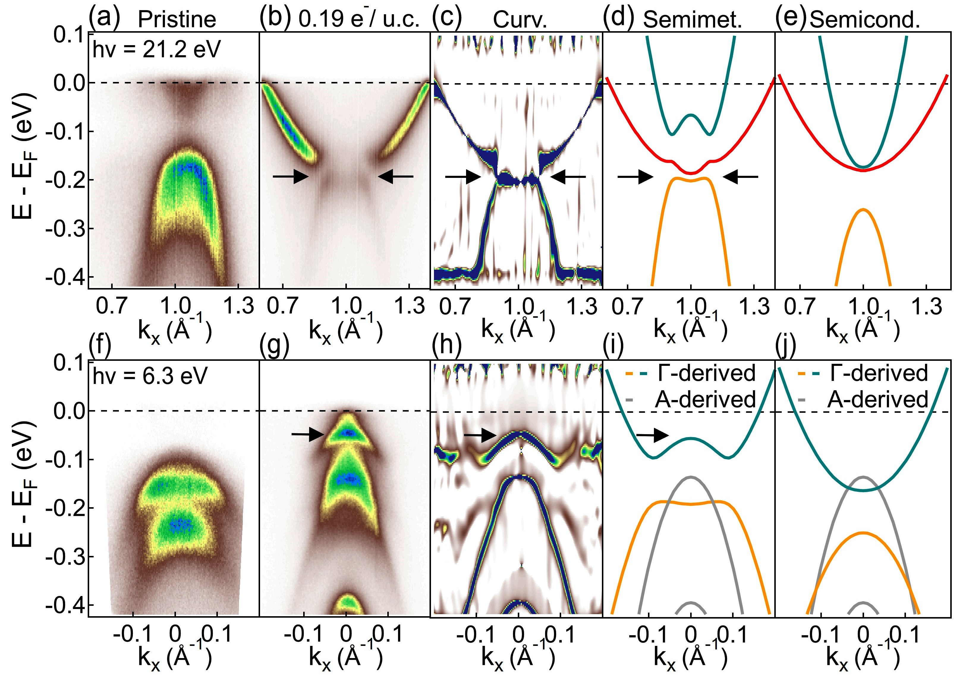
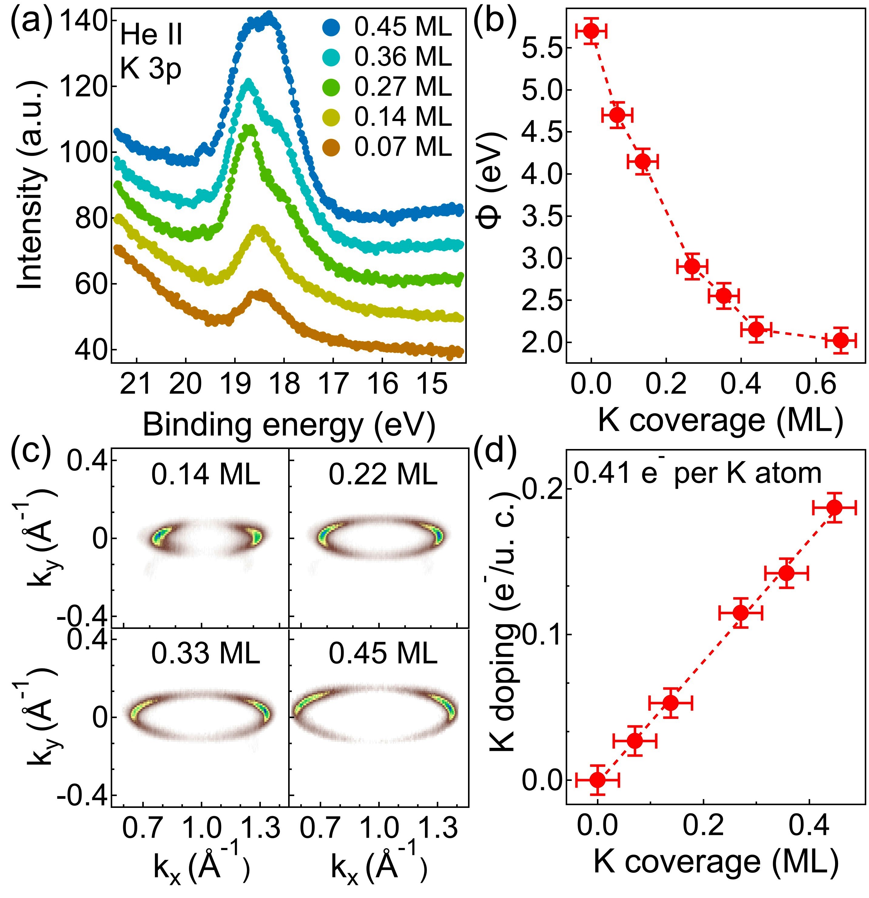
Figure 2(a) shows the evolution of the K 3 shallow core level upon sequential K evaporations at T40 K on 1-TiSe2 measured using He-II photon energy (= eV). For K coverages lower than 0.10 ML (1 ML corresponds to one K atom per 1-TiSe2 surface unit cell), the photoemission spectrum mainly consists of one component at 18.4 eV BE associated with 2D dispersed K atoms. With increased coverages, a second component corresponding to closely packed K atoms continuously grows on the low BE side (17.9 eV BE) and starts to be dominant at 0.45 ML coverage as the dispersed alkali atoms begin to condense into metallic islands in close analogy with the mechanism of LT K adsorption on graphite Caragiu and Finberg (2005). The work function of 1-TiSe2 changes continuously as a function of the K coverage [Fig. 2(b)] 333The work function, defined as the energy of the vacuum level with respect to , is determined from the low-energy cut off of the secondary photoelectron emission. To this end, the samples were biased at -8V to make the measurements of the very low-energy region of the spectrum reliable., and exhibits no minimum, but a saturation after the K deposition of 0.45 ML at the K bulk value (1.8 eV). Most of the work function decrease occurs within the first 0.30 ML, indicating a strong electron transfer from the alkali atoms in the 2D dispersed phase to the surface.
The surface doping can be calculated from the Luttinger area of the LT FS at that expands upon K deposition (, where = 3 is the valley multiplicity for all occupied Ti 3 electron pockets, and and kL are their short and long axes lengths)[Fig. 2(c)]. As shown in Fig. 2(d), the surface electron doping linearly increases with the K coverage and has a value of 0.19 per unit cell at 0.45 ML, which is more than three times the critical doping of 0.06 per unit cell at which the superconductivity emerges in Cu-intercalated 1-TiSe2 Morosan et al. (2006), but is similar to that obtained in thin TiSe2 films grown on TiO2 Jia et al. (2018). In this range of coverage, there is a constant charge transfer from K to the 1-TiSe2 surface of 0.41 per K atom demonstrating that a rigid band model of electron doping applies.
Having demonstrated that LT K depositions effectively strongly electron-dope the 1-TiSe2 surface, let us now focus on the CDW state. Figure 3(a) shows ARPES intensity map of pristine 1-TiSe2 taken at T = 30 K using He-I radiation (= eV) that probes the initial states close to the point of the 3D BZ in a free-electron final-state picture Pillo et al. (2000). We clearly see the well-known backfolding of the topmost Se 4 hole band coming from the point as well as the Ti electron pocket that derives purely from the orbital projection of the conduction bands and remains unaffected by the CDW phase transition Watson et al. (2019); Jaouen et al. (2019). Upon strong K doping [0.19 per unit cell, Fig. 1(b)], the Ti 3 band at rigidly shifts by 180 meV towards higher BE and starts to overlap with the backfolded hole band due to the reduced (also manifested by the strongly lowered spectral weight of the backfolding), resulting in band gap openings at the avoided band crossings [see black arrows on Fig. 3(b)-(d)].
From Fig. 1, the conclusion is clear: the presence of an energy gap at the band crossings and the flattened band dispersion [see the curvature plot, Fig. 3(c), extracted from the ARPES intensity map Zhang et al. (2011)] are only compatible with an initial semimetallic band configuration as exemplified by the direct comparison of the calculated band dispersions of the semimetal and semiconductor cases [Fig. 3(d) and (e), respectively]444The band is not shown here since it has been demonstrated to carry no spectral weight for every along the and directions within the effective Hamiltonian model of the four interacting bands of 1-TiSe2 Monney et al. (2009). Our calculated band dispersions for the semimetal indeed allow to track both the band gap opening [see black arrows in Fig. 3(d)], and the specific shape and BE of the backfolded hole band [orange band dispersion in Fig. 3(d)]. On the contrary, in the semiconducting case, the CDW band gap cannot be smaller than the initial band gap such that - band crossings can not occur resulting in a backfolding BE much higher than in experiment.
In contrast to the backfolded hole band and in agreement with the calculated spectral function [Fig. 1(d)], the Mexican hat [green band dispersion in Fig. 3(d)], hardly distinguishable on the curvature plot [Fig. 3(c)], carries extremely weak spectral weight at . This is a strong indication that the hybridization between the hole band at and the electron one at at the CDW phase transition is accompanied by band inversion. In fact, the Mexican hat corresponds to the top of the original hole band split by the CDW and mainly derives from the Se 4 orbitals, whereas the top of the backfolded hole band is associated with the bottom of the original Ti 3 electron bands. From this, we can explain the strong photoemission intensity of the umklapp of Ti 3 orbital character at and anticipate that the Se 4-derived Mexican hat should appear more clearly at the point since the spectral weight as seen by ARPES also follows the projection of the states onto the non-reconstructed zone Voit et al. (2000).
Laser-based ARPES measurements (= eV) at normal emission [Fig. 3(f)-(g)] indeed reveal clear changes in the photoemission spectral weight. Whereas for pristine 1-TiSe2 [Fig. 3(f)], one can easily recognize the Se 4 valence bands coming from the point with a characteristic flattening of the topmost band, upon K doping [Fig. 3(g)], the Mexican hat, which has shifted below , becomes intense [black arrows] and the backfolded band has almost no spectral weight [see Fig. 3(h) and the orange band in Fig. 3(i)]. Interestingly, two new hole bands with significant spectral weight now appear in the photoemission intensity map. From our DFT-calculated band structures 555see Supplemental material, we can attribute them to the two Se 4 valence bands derived from the point which can be probed in laser-ARPES due to final-state effect of photoemission beyond the free-electron final state approximation Lindroos and Bansil (1996). Indeed, at such low photon energy, it is known that direct transitions to unoccupied Bloch-like states are allowed in a large portion of the BZ along Xiong et al. (2017).
In our case, the -derived valence bands allow for accessing the - dispersion in the ARPES intensity map of the K-doped CDW state and definitively demonstrate that the 1-TiSe2 normal state is semimetallic. Looking at the semiconducting case in Fig. 3(j), the agreement with the experimental band dispersions is poor, namely the absence of the Mexican hat and the presence of a slight - band overlap in the - plane of the BZ [Fig. 3(j)]. Furthermore, our measurements also solve the puzzling observation of Ref.Watson et al. (2019), namely a decreased gap at LT between the -derived and the unhybridized Ti 3 passenger states at that determine the band gap in the CDW phase. Starting with a semimetallic normal state, the slightly overlapping bands of the - plane also open a small gap (15 meV) through the CDW phase transition.

Finally, we show in Fig. 4(a) the ARPES intensity maps at the point of the BZ upon gradual K doping. The near- band dispersions calculated within our effective Hamiltonian model of four bands in a semimetallic band configuration with an overlap of 110 meV and interacting through are also superimposed. Together with the gradual filling of the Ti 3 electron band that linearly shifts with doping (red bands), we can track the CDW gap closure. Figure 4(b) shows the evolution of the BEs of the Mexican hat (green bands) and backfolding (orange bands) corrected by as extracted from the BE shift of the Ti 3 band (red bands) as a function of K doping. We clearly see that, with increased K doping and decreasing , the Mexican hat and the backfolding band symmetrically shift towards the asymptotic limit of vanishing corresponding to the semimetallic 1-TiSe2 normal state where they respectively correspond to the top and the bottom of the overlapping Se 4 and Ti 3 bands [red-dashed lines on Fig. 4(b)].
Our unambiguous demonstration of the semimetallic normal-state of 1-TiSe2 not only closes a long-standing debate, but is also of crucial importance for the understanding of the CDW instability and the closely related emergence of inhomogeneous superconducting states in electron-doped and pressurized compounds. By demonstrating that 1-TiSe2 has a well defined FS in its normal state, our study strongly supports the recently proposed mechanism for both the CDW instability and the emergence of phase-separated states upon doping based on imperfect ”nesting” of FS hotspots, i.e. band crossings at the Fermi level Jaouen et al. (2019).
Acknowledgements.
This project was supported by the Fonds National Suisse pour la Recherche Scientifique through Div. II and Grant No. P00P2_170597. Skillful technical assistance was provided by F. Bourqui, B. Hediger and O. Raetzo.References
- Morosan et al. (2006) E. Morosan, H. W. Zandbergen, B. S. Dennis, J. W. G. Bos, Y. Onose, T. Klimczuk, A. P. Ramirez, N. P. Ong, and R. J. Cava, Nat. Phys. 2, 544 (2006).
- Sipos et al. (2008) B. Sipos, A. F. Kusmartseva, A. Akrap, H. Berger, L. Forró, and E. Tutiš, Nat. Mater. 7, 960 (2008).
- Kusmartseva et al. (2009) A. F. Kusmartseva, B. Sipos, H. Berger, L. Forró, and E. Tutiš, Phys. Rev. Lett. 103, 236401 (2009).
- Novoselov et al. (2016) K. S. Novoselov, A. Mishchenko, A. Carvalho, and A. H. Castro Neto, Science 353, 461 (2016).
- Wilson and Yoffe (1969) J. Wilson and A. Yoffe, Adv. Phys. 18, 193 (1969).
- Li et al. (2015) L. J. Li, E. C. T. O’Farrell, K. P. Loh, G. Eda, B. Özyilmaz, and A. H. Castro Neto, Nature (London) 529, 185 (2015).
- Jaouen et al. (2019) T. Jaouen, B. Hildebrand, M.-L. Mottas, M. Di Giovannantonio, P. Ruffieux, M. Rumo, C. W. Nicholson, E. Razzoli, C. Barreteau, A. Ubaldini, E. Giannini, F. Vanini, H. Beck, C. Monney, and P. Aebi, Phys. Rev. B 100, 075152 (2019).
- Di Salvo et al. (1976) F. Di Salvo, D. Moncton, and J. Waszczak, Phys. Rev. B 14, 4321 (1976).
- Wilson et al. (1978) J. A. Wilson, A. S. Barker, F. J. Di Salvo, and J. A. Ditzenberger, Phys. Rev. B 18, 2866 (1978).
- Li et al. (2007) G. Li, W. Z. Hu, D. Qian, D. Hsieh, M. Z. Hasan, E. Morosan, R. J. Cava, and N. L. Wang, Phys. Rev. Lett. 99, 027404 (2007).
- Velebit et al. (2016) K. Velebit, P. Popčević, I. Batistić, M. Eichler, H. Berger, L. Forró, M. Dressel, N. Barišić, and E. Tutiš, Phys. Rev. B 94, 075105 (2016).
- Rossnagel et al. (2002) K. Rossnagel, L. Kipp, and M. Skibowski, Phys. Rev. B 65, 235101 (2002).
- Kidd et al. (2002) T. E. Kidd, T. Miller, M. Y. Chou, and T.-C. Chiang, Phys. Rev. Lett. 88, 226402 (2002).
- Zhao et al. (2007) J. F. Zhao, H. W. Ou, G. Wu, B. P. Xie, Y. Zhang, D. W. Shen, J. Wei, L. X. Yang, J. K. Dong, M. Arita, H. Namatame, M. Taniguchi, X. H. Chen, and D. L. Feng, Phys. Rev. Lett. 99, 146401 (2007).
- Rasch et al. (2008) J. C. E. Rasch, T. Stemmler, B. Müller, L. Dudy, and R. Manzke, Phys. Rev. Lett. 101, 237602 (2008).
- Chen et al. (2016) P. Chen, Y.-H. Chan, X.-Y. Fang, S.-K. Mo, Z. Hussain, A.-V. Fedorov, M. Y. Chou, and T.-C. Chiang, Sci. Rep. 6, 37910 (2016).
- Watson et al. (2019) M. D. Watson, O. J. Clark, F. Mazzola, I. Marković, V. Sunko, T. K. Kim, K. Rossnagel, and P. D. C. King, Phys. Rev. Lett. 122, 076404 (2019).
- Monney et al. (2015) G. Monney, C. Monney, B. Hildebrand, P. Aebi, and H. Beck, Phys. Rev. Lett. 114, 086402 (2015).
- Monney et al. (2012a) C. Monney, G. Monney, P. Aebi, and H. Beck, Phys. Rev. B 85, 235150 (2012a).
- Borisenko et al. (2008) S. V. Borisenko, A. A. Kordyuk, A. N. Yaresko, V. B. Zabolotnyy, D. S. Inosov, R. Schuster, B. Büchner, R. Weber, R. Follath, L. Patthey, and H. Berger, Phys. Rev. Lett. 100, 196402 (2008).
- Pillo et al. (1999) T. Pillo, J. Hayoz, H. Berger, M. Grioni, L. Schlapbach, and P. Aebi, Phys. Rev. Lett. 83, 3494 (1999).
- Monney et al. (2012b) C. Monney, G. Monney, P. Aebi, and H. Beck, New J. Phys. 14, 75026 (2012b).
- Note (1) Details on the model from which the near- dispersions and spectral functions describing ARPES have been computed can be found in Refs. Monney et al. (2009); Jaouen et al. (2019).
-
Note (2)
In a photoemission experiment, we can extract the order
parameter from the shift of the backfolded valence band, using,
where is the band overlap ( 0) or band gap ( 0) in the normal state.Jaouen et al. (2019).(2) - Monney et al. (2009) C. Monney, H. Cercellier, F. Clerc, C. Battaglia, E. F. Schwier, C. Didiot, M. G. Garnier, H. Beck, P. Aebi, H. Berger, L. Forró, and L. Patthey, Phys. Rev. B 79, 045116 (2009).
- Qian et al. (2007) D. Qian, D. Hsieh, L. Wray, E. Morosan, N. L. Wang, Y. Xia, R. J. Cava, and M. Z. Hasan, Phys. Rev. Lett. 98, 117007 (2007).
- Hildebrand et al. (2017) B. Hildebrand, T. Jaouen, C. Didiot, E. Razzoli, G. Monney, M.-L. Mottas, F. Vanini, C. Barreteau, A. Ubaldini, E. Giannini, H. Berger, D. R. Bowler, and P. Aebi, Phys. Rev. B 95, 081104(R) (2017).
- Hildebrand et al. (2016) B. Hildebrand, T. Jaouen, C. Didiot, E. Razzoli, G. Monney, M.-L. Mottas, A. Ubaldini, H. Berger, C. Barreteau, H. Beck, D. R. Bowler, and P. Aebi, Phys. Rev. B 93, 125140 (2016).
- Hildebrand et al. (2014) B. Hildebrand, C. Didiot, A. M. Novello, G. Monney, A. Scarfato, A. Ubaldini, H. Berger, D. R. Bowler, C. Renner, and P. Aebi, Phys. Rev. Lett. 112, 197001 (2014).
- Rossnagel (2010) K. Rossnagel, New J. Phys. 12, 125018 (2010).
- Caragiu and Finberg (2005) M. Caragiu and S. Finberg, Journal of Physics: Condensed Matter 17, R995 (2005).
- Note (3) The work function, defined as the energy of the vacuum level with respect to , is determined from the low-energy cut off of the secondary photoelectron emission. To this end, the samples were biased at -8V to make the measurements of the very low-energy region of the spectrum reliable.
- Jia et al. (2018) T. Jia, S. N. Rebec, S. Tang, K. Xu, H. M. Sohail, M. Hashimoto, D. Lu, R. G. Moore, and Z.-X. Shen, 2D Materials 6, 011008 (2018).
- Pillo et al. (2000) T. Pillo, J. Hayoz, H. Berger, F. Lévy, L. Schlapbach, and P. Aebi, Phys. Rev. B 61, 16213 (2000).
- Zhang et al. (2011) P. Zhang, P. Richard, T. Qian, Y.-M. Xu, X. Dai, and H. Ding, Review of Scientific Instruments 82, 043712 (2011).
- Note (4) The band is not shown here since it has been demonstrated to carry no spectral weight for every along the and directions within the effective Hamiltonian model of the four interacting bands of 1-TiSe2 Monney et al. (2009).
- Voit et al. (2000) J. Voit, L. Perfetti, F. Zwick, H. Berger, G. Margaritondo, G. Grüner, H. Höchst, and M. Grioni, Science 290, 501 (2000).
- Note (5) See Supplemental material.
- Lindroos and Bansil (1996) M. Lindroos and A. Bansil, Phys. Rev. Lett. 77, 2985 (1996).
- Xiong et al. (2017) H. Xiong, J. A. Sobota, S.-L. Yang, H. Soifer, A. Gauthier, M.-H. Lu, Y.-Y. Lv, S.-H. Yao, D. Lu, M. Hashimoto, P. S. Kirchmann, Y.-F. Chen, and Z.-X. Shen, Phys. Rev. B 95, 195119 (2017).
Supplemental Material: Unveiling the Semimetallic Nature of 1-TiSe2 by Doping its Charge Density Wave
T. Jaouen,1 M. Rumo,1 B. Hildebrand,1 M.-L. Mottas,1 C. W. Nicholson,1 G. Kremer,1
B. Salzmann,1 F. Vanini,1 C. Barreteau,2 E. Giannini,2 H. Beck,1 P. aebi,1 and C. Monney5
1Département de Physique and Fribourg Center for Nanomaterials,
Université de Fribourg, CH-1700 Fribourg, Switzerland
2Department of Quantum Matter Physics, University of Geneva,
24 Quai Ernest-Ansermet, 1211 Geneva 4, Switzerland
.1 DFT computational details
The DFT-calculated unfolded band structures of the 2 2 2 CDW phase have been obtained within the WIEN2K package Blaha et al. (2001), using the modified Becke-Johnson (mBJ) exchange potential in combination with local density approximation (LDA) correlation Tran and Blaha (2009); Koller et al. (2012). Our calculations include spin-orbit coupling (SOC) that has been shown to be crucial for a good description of the Se 4 hole bands along - in the TiSe2 normal state Vydrova et al. (2015); Ghafari et al. (2017). The tuning parameter of the mBJ functional is related to the average value of by where is the electron density, and two free parameters and an empirical exponent Koller et al. (2012). In our calculations, has been fixed for all calculations at 1.34, the value determined to give the best agreement with the measured normal-state band structure of 1-TiSe2 and a minimum of the total energy for atomic displacements corresponding to the periodic lattice distortion (PLD) as proposed by Di Salvo Di Salvo et al. (1976). The system was modeled using a 2 2 2 superstructure of 8 unit cells of TiSe2 with lattice parameters set to ==3.54 Å and =6.01 Å Di Salvo et al. (1976). The calculated band structures were unfolded using the FOLD2BLOCH package Rubel et al. (2014).

.2 In and out-of-plane DFT-calculated band dispersions as a function of the CDW order parameter
At K, 1-TiSe2 undergoes a phase transition towards a 2 2 2 commensurate inversion-symmetric CDW phase Hildebrand et al. (2018). A weak PLD develops involving energetically favorable Ti-Se bond shortening of of the Ti atoms of the unit cell and a rotation of the Se atoms around the remaining Whangbo and Canadell (1992); Di Salvo et al. (1976) [Fig. SS1 (a)]. It has been shown that the magnitude of the Ti-Se bond shortening can be associated with the CDW order parameter as it follows a mean-field-like evolution as a function of temperature, characteristic of a second-order phase transition Di Salvo et al. (1976). In our DFT calculations we therefore vary the amplitude of the PLD in order to study the impact of the reduction induced by K doping on the electronic band dispersions along the and directions of the 3D BZ [Fig. SS1 (b)].
Fig. SS1 (c) and SS1 (d) respectively show the in-plane and out-of-plane DFT-calculated band dispersions of 1-TiSe2 of the non-distorted state (no PLD, red color scale) and fully distorted (100 PLD, blue color scale) CDW phase. The color scale represents the distribution of spectral weight. The band structure of the fully hybridized CDW state have been shifted in energy in order to align the bottom of the Ti 3 conduction bands with the one of the non-distorted state as its binding energy remains unaffected by the CDW phase transition (see main text).
In very good agreement with experiment [Fig. 3(a) of the main text], we see on Fig. SS1 (c) the appearance, upon the PLD, of the renormalization of the Ti 3 electron band at the -vectors of the - band crossings Jaouen et al. (2019), and of the backfolding of the two Se 4 hole bands coming from the point [Se 4 (1) and Se 4 (2)]. From the calculated - dispersions [Fig. SS1 (d)], we see that the CDW phase transition is accompanied by an overall energy shift towards higher binding energy of the Se 4 bands as well as a strong flattening of the topmost hole band [Se 4 (1)], that becomes quasi two-dimensional (2D). Comparing the binding energies of the backfolded band extrema at Fig. SS1 (c) with those at [Fig. SS1 (d)], demonstrates that the heaviest Se 4 band at [Se 4 (2)] corresponds to the hole band at which does not play a role in the CDW ordering and has a Se 4 character Watson et al. (2019). The hole band of lower effective mass that appears at higher binding energy in Fig. SS1 (c) [Se 4 (1)] is associated with the 2D hole band of orbital character. Note that introducing the PLD in the DFT calculations that give a semimetallic normal state with a significant - band overlap (170 meV) is sufficient to nicely match the experimental band dispersions of the CDW state.
Fig. SS1 (e) and SS1 (f) focus on the in-plane and out-of-plane DFT band structures for slightly displaced atoms (25 PLD, orange color scale), corresponding to the reduction induced by the strongest K-doping of 0.19 per unit cell. Since the Ti 3 band at rigidly shifts towards higher binding energy upon doping, the band structures have been shifted to take into account the chemical potential change of 180 meV after a first alignment of the bottom of the Ti 3 conduction bands with the one of the non-distorted state. Overall, the in-plane DFT-calculated band dispersions [Fig. SS1 (e)] very well reproduce the main spectroscopic features of the ARPES intensity map of the K-doped sample measured at using He-I radiation [Fig. 3(b) of the main text]; namely, the band binding energies, the effective masses, as well as the spectral weights. The backfolded hole bands [Se 4 (1), (2)] are now nearly-degenerated at , the spectral weight of the Ti 3 band reduces approaching the point and the Mexican hat is almost not visible. On the contrary, the latter appears clearly in the DFT calculations at the point [green Se 4 (1) in Fig. SS1 (f)] as in the laser-based photoemission experiment [Fig. 3(g) and (h) of the main text]. Looking at the dispersion along - Fig. SS1 (f), finally allows to demonstrate that the two new hole bands with significant spectral weight appearing in the photoemission intensity map using 6.3 eV photon energy [Fig. 3(g) and (h) of the main text] are the Se 4 valence bands derived from the point [black Se 4 (1) and Se 4 (2)]. Indeed, both the spectral weights of the hole bands at the and the points and the alternation of the band extrema [see the green, orange and grey circles on Fig. SS1(f) that respectively indicate the extrema of the and -derived bands and Fig. 3(i) of the main text] well correspond to our laser-ARPES data.
To summarize, our ARPES data, the simulated near- dispersions and the unfolded DFT band structure calculations are in excellent agreement and allow for demonstrating final-state effects of photoemission beyond the free-electron final state approximation Lindroos and Bansil (1996) in our laser-based photoemission data. Direct transitions from both the and the -derived valence bands to Bloch-like final states allow for accessing the - dispersion in the ARPES intensity map of the K-doped CDW state.
References
- Blaha et al. (2001) P. Blaha, K. Schwarz, G. K. H. Madsen, D. Kvasnicka, and J. Luitz, WIEN2K, An Augmented Plane Wave + Local Orbitals Program for Calculating Crystal Properties (Karlheinz Schwarz, Techn. Universität Wien, Austria, 2001).
- Tran and Blaha (2009) F. Tran and P. Blaha, Phys. Rev. Lett. 102, 226401 (2009).
- Koller et al. (2012) D. Koller, F. Tran, and P. Blaha, Phys. Rev. B 85, 155109 (2012).
- Vydrova et al. (2015) Z. Vydrova, E. F. Schwier, G. Monney, T. Jaouen, E. Razzoli, C. Monney, B. Hildebrand, C. Didiot, H. Berger, T. Schmitt, V. N. Strocov, F. Vanini, and P. Aebi, Phys. Rev. B 91, 235129 (2015).
- Ghafari et al. (2017) A. Ghafari, L. Petaccia, and C. Janowitz, Appl. Surf. Sci. 396, 1649 (2017).
- Di Salvo et al. (1976) F. Di Salvo, D. Moncton, and J. Waszczak, Phys. Rev. B 14, 4321 (1976).
- Rubel et al. (2014) O. Rubel, A. Bokhanchuk, S. J. Ahmed, and E. Assmann, Phys. Rev. B 90, 115202 (2014).
- Hildebrand et al. (2018) B. Hildebrand, T. Jaouen, M.-L. Mottas, G. Monney, C. Barreteau, E. Giannini, D. R. Bowler, and P. Aebi, Phys. Rev. Lett. 120, 136404 (2018).
- Whangbo and Canadell (1992) M. H. Whangbo and E. Canadell, J. Am. Chem. Soc. 114, 9587 (1992).
- Jaouen et al. (2019) T. Jaouen, B. Hildebrand, M.-L. Mottas, M. Di Giovannantonio, P. Ruffieux, M. Rumo, C. W. Nicholson, E. Razzoli, C. Barreteau, A. Ubaldini, E. Giannini, F. Vanini, H. Beck, C. Monney, and P. Aebi, Phys. Rev. B 100, 075152 (2019).
- Watson et al. (2019) M. D. Watson, O. J. Clark, F. Mazzola, I. Marković, V. Sunko, T. K. Kim, K. Rossnagel, and P. D. C. King, Phys. Rev. Lett. 122, 076404 (2019).
- Lindroos and Bansil (1996) M. Lindroos and A. Bansil, Phys. Rev. Lett. 77, 2985 (1996).