DOI: 10.1002/adem.201900991
Article type: Communication
Record-Breaking Magnetoresistance at the Edge of a Microflake of Natural Graphite
Keywords: Natural Graphite, Internal Interfaces, Magnetoresistance, High Magnetic Field
Placing several electrodes at the edge of a micrometer-size Sri Lankan natural graphite sample at distances comparable to the size of the internal crystalline regions, we found record values for the change of the resistance with magnetic field. At low temperatures and at T the magnetoresistance (MR) reaches %. The MR values exceed by far all earlier reported ones for graphite and they are comparable or even larger (at K) than the largest reported in solids including the Weyl semimetals. The origin of this large MR lies in the existence of highly conducting 2D interfaces aligned parallel to the graphene planes.
The electrical transport properties of bulk graphite, multigraphene and single graphene layers show a variety of interesting phenomena. These phenomena are expected to be of advantage for applications such as solar cells, supercapacitors, flexible transistors and sensors.1, 2 These perspectives in addition to the high carbon abundance in nature still attract the interest of the scientific community. In particular a detailed understanding of the electronic properties of multigraphene samples is currently of high relevance because of the expected unique properties of the electronic band structure. We refer to stacked graphene layers that can lead to the formation of flat bands, i.e., a region in reciprocal space with a dispersionless relationship, opening the possibility of triggering high-temperature superconductivity or magnetic order.3 This can happen at certain localized regions of twisted graphene layers like in bilayers graphene or at embedded interfaces between twisted Bernal or rhombohedral stacking order regions in graphite or multigraphene samples.4, 5, 6, 7
In this work we studied graphite samples, which are formed by stacking graphene layers held together by weak Van der Waals forces. The stacking order of the layers occurs naturally in two different ways: the hexagonal one, named Bernal with the graphene layer order ABABA… (2H), and the rhombohedral ABCABCA… (3R). Several scanning transmission electron microscope (STEM) images of the internal structure of usual graphite samples were published in the last 10 years, showing their inhomogeneity due to existence of crystalline regions of different thicknesses with different stacking orders or twisted regions at different angles around the common axis.6
Since the 80’s and partially due to the increasing structural order and quality of the measured graphite samples, the maximum magnetoresistance (MR) found for graphite samples steadily increased.8 Recently published systematic studies of the MR of graphite samples of different thickness revealed that this property is directly related to the existence of two-dimensional (2D) interfaces between crystalline regions with Bernal or rhombohedral stacking order. These 2D interfaces are also responsible for the metalliclike behavior of the resistance of graphite.9, 10 The MR of graphite samples we discuss in this work is always measured at fields normal to the interfaces and the graphene planes. The MR for parallel fields is negligible or related to a normal field component due to misalignment, which can come also from the angle distribution of the internal crystalline regions (finite rocking curve width).11
Attempting to understand the nature behind the internal structure of graphite and to find a way to increase its MR further, we have performed transport measurements under pulsed magnetic fields up to 65 T, placing the voltage electrodes on the sample edge at one side of the sample. This enables the possibility to obtain signals to a greater extend related to the interfaces contribution, at least at temperatures K where the total conductance of the interfaces exceeds that of the semiconducting 2H and/or 3R matrix.10
From electron back scattering diffraction (EBSD) measurements on graphite samples we know that the single crystalline regions, in the planes of well-ordered bulk graphite samples are m, whereas the coherent regions along the axis direction range from a few nm to several 100 nm.6, 12 The distance between grain boundaries within a single interface puts an upper limit to the typical length of the internal interfaces found in graphite samples. Therefore, in order to decrease the contribution from the grain boundaries, we need to place the voltage electrodes at distances smaller than m. We found that placing the voltage electrodes at the sample edge, contacting as many interfaces edges as possible and at small enough distances comparable to the extension of a 2D interface region, the obtained MR values are much larger than the ones reported for graphite, multigraphene or other carbon-based materials before. The obtained MR turned out to be of the order or larger than the largest reported nowadays in solids. The technical simplification we present in this study provides a convenient and relatively easy way to study the response of 2D interfaces with their unconventional properties.
The electrical resistance at different positions along the sample edge was measured using four terminals. The electrodes were made combining electron beam lithography and sputtering of Cr/Au. The aim was to place the voltage electrodes at the edge of the thin sample in order to directly contact a large number of interface edges present in the sample (see, e.g., the STEM images of different graphite samples in Ref. 6). Micrometer-sized samples with well-defined interface edges are not easy to prepare. One way is to produce TEM lamellae as studied by Ballestar et al., but their production for transport measurements is very difficult, taking usually several months of preparation to get a single sample.13 In order to overcome these difficulties, we have developed a new method to produce graphite flakes with well-defined edges, avoiding problems of contamination or formation of an amorphous thin layer.
On the top of a mm2 silicon substrate with a thickness of 0.525 mm and covered with a 150 nm silicon nitride () insulating layer, we placed micro-flakes of Sri Lankan natural graphite (NG). The samples were from the same batch of samples analyzed with STEM, XRD and PIXE published recently. 14 After selecting flat enough samples, we covered part of the sample surfaces with a 200 nm thick film using electron beam lithography (see the sketch in Figure 1(a) and (b)).
An Oxford Instruments Plasma Pro NGP80 ICP device was used to etch the sample with inductively coupled plasma (ICP) reactive ion etching (RIE). This process is very effective to remove graphene layers in graphite samples in a controlled way.7, 15, 16, 17 In this way the area of the sample not covered by the film was completely removed, creating a sharp and well-defined edge. The area protected by remained after RIE (Figure 1(c)). The parameters used for RIE were 282 V for the applied DC Bias, 50 W HF power, 50 W ICP power, mbar as chamber pressure, 9 sccm for Ar and 1 sccm gas flow rate. Under these parameters, we could completely etch through a 665 nm thick graphite sample in 40 min.
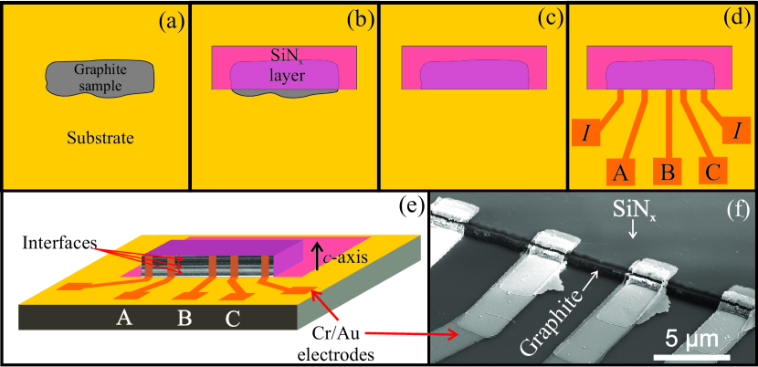
After etching the sample, electrodes were deposited on the lateral part of the sample (see Figure 1(d-f)), parallel to the axis and contacting the interfaces edges. Electron beam lithography was used to prepare the electrodes, where a chromium thin film with thickness of 5 nm was sputtered first and then a 50 nm gold film on top. The main sample shown here, labeled U11, had in total 5 electrodes (each 2.5 m width), allowing electrical transport measurement at different regions of the sample (see Figure 1 (d-f)). The temperature and magnetic field dependence of the resistance to 7 T were measured in a Quantum Design 4He flow cryostat with a superconducting solenoid, with a high-resolution AC resistance bridge LR-700 at a frequency of 19 Hz and input current of 12 A.
The measurements at high magnetic fields were performed at the pulsed field facility of the NHMFL at Los Alamos National Laboratory in a 3He + 4He cryostat with maximum magnetic field of 65 T. Most of the experiments were performed with pulses of 60 T. A down-sweep pulse lasts approximately 60 ms, wherever the up-sweep peak field is reached at 10 ms. An AC current of 12 A was applied to the sample at a frequency of 50.5 kHz ( for further details see the supporting information (SI)). The voltages were measured with a 20 MHz sampling rate. The field was always applied normal to the graphene planes and 2D interfaces.
In order to minimize the noise on the measurement, we used copper wires with diameter of 60 m, tightly twisted in pairs, with 3-4 windings per mm. We used one pair to apply the current and two other pairs to read the voltages. The wire-pairs were glued with GE varnish on the walls of the rod used to insert the sample inside the cryostat, reducing the noise introduced by vibrations due to the pulse. Other source of noise in this kind of measurements are the open loops (untwisted parts of the wires) due to the high . To minimize this effect we fixed the twisted wires as close as possible to the sample. Low field measurements were performed on three samples. In the main article we will show and discuss the one with the highest MR. The results of the other samples can be seen in the SI where we include further details of the samples purity.
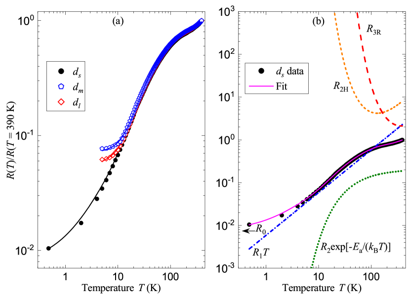
The temperature dependence of the normalized resistance at zero field for sample U11 is shown in Figure 2. The data are labeled according to the distance between the voltage reading electrodes, e.g., the data labeled were obtained between the electrodes B and C with the shortest distance (see Figure 1(e)). The temperature dependence shown in Figure 2 follows the usual metalliclike behavior of well-ordered bulk graphite samples in all temperature range, indicating that the electrodes are sensing regions containing 2D interfaces.9, 10, 7
The results plotted in Figure 2 (a) show that all three curves are similar between K to 15 K. At lower temperatures, the results labeled and tend clearly to saturate due to the contribution of a residual resistance attributed to the scattering of conduction electrons at the grain boundaries, in agreement with a large number of published data. In this temperature region and in contrast to the other two configurations, the curve is remarkably different exhibiting a much lower residual resistance. The resistance ratio (390 K)(5 K) for , and are 29, 13, and 16, respectively. The resistance ratio increases further for the configuration only, reaching a remarkable high value of (390 K)(0.48 K) 100. The observed behavior implies that the sample is not homogeneous, in agreement with studies realized in the last years on different graphite samples.13, 7
The temperature dependence of the resistance is fitted using a phenomenological parallel resistor model as proposed first in Ref. 9 and extended in following years.10, 7 The model takes explicitly into account the internal structure of real graphite samples, assuming three contributions in parallel. The first one due to the embedded 2D interfaces provides the metalliclike behavior of graphite; the second and third ones are the semiconducting contributions of the hexagonal 2H and rhombohedral 3R stacking orders, see the SI for details of the model. The metalliclike contribution is composed by a temperature independent residual resistance, a linear and a thermally activated temperature dependent term. Such phenomenological model describes with good accuracy the temperature dependence of the resistance in the entire investigated temperature range. Note that below 200 K, the interface contribution is the most important one and the fit is not very sensitive to the parameters of the other two contributions, see Figure 2(b). A detailed discussion on this issue and on the weight of the parameters in a given temperature range was published recently.10 The values of the fit parameters can be seen in the SI. As expected, the residual resistance from the fit at the low temperature of the data shown in Figure 2(a) is one order of magnitude smaller than for and . From the fits of the data to the parallel resistor model we find that the linear-in-temperature term of the interface contribution10 is important at K, whereas the thermally activated exponential term (with an excitation energy of the order of meV) clearly contributes between 15 K and K. It is interesting to note that the low residual resistance of the data clearly reveals the linear-in-temperature contribution that holds to the lowest measured temperature. The temperature dependence of the resistance at different constant applied magnetic fields for the three configurations of sample U11, the field-driven metal-insulator transition and the Shubnikov-de Haas (SdH) oscillations are discussed in the SI.
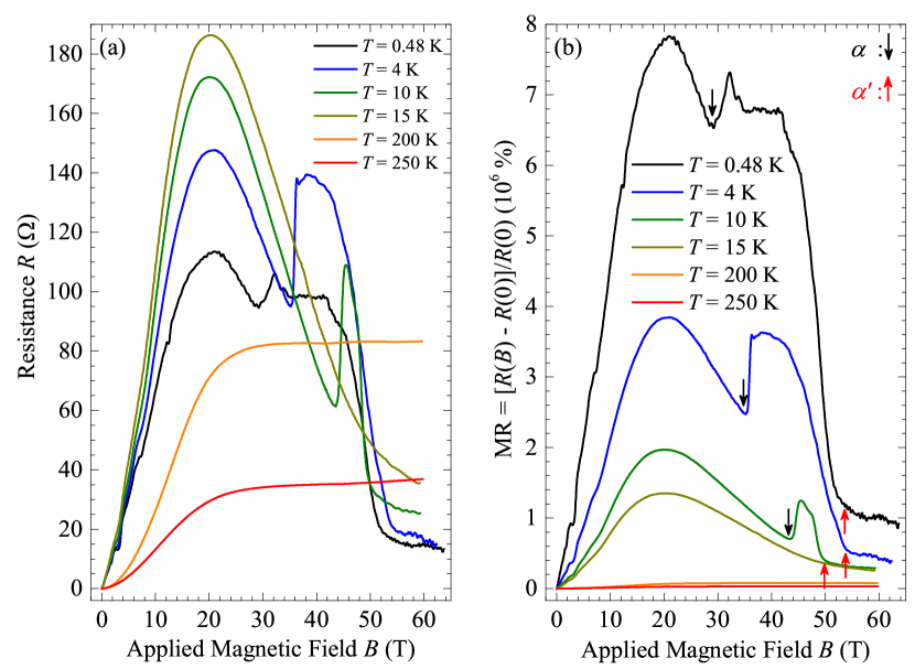
We discuss now the field dependence of the resistance and the MR defined as MR , where is the measured resistance at zero applied magnetic field (MR ). As shown in the SI, and as example, at K and T the MR reaches % at the contacts and . For the contact configuration the MR is nearly twice larger reaching %, see Figure 3 for the results obtained with pulsed fields. Earlier studies in high quality graphite samples show a MR of 15,500 %, 14,000 %, 400 %, and 75 %.7, 19, 20, 21 In graphene/boron-nitride heterostructures a MR of 90,000 % was measured at similar field and temperature22, see Figure 4(a).
Figure 3 shows the high field results obtained in the configuration; panel (a) shows the absolute resistance and panel (b) the MR at different constant temperatures. The up and down arrows in (b) indicate the fields at which the commonly reported electronic high field transitions and of graphite occur at K. These transitions as well as the maximum and negative MR above 20 T are related to the electronic 2D systems of some interfaces in the sample and were discussed in detail in a recent publication. 4 The MR at K and T reaches %, exceeding by far all values reported for graphite in literature.
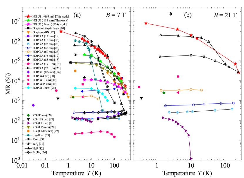
A comparison with the temperature dependence of the MR data reported for different graphite samples in the literature and at fields of 7 T and 21 T, is given in Figure 4(a) and (b).24, 25, 26, 27, 28, 29, 30 Large MR values were observed for Type-II Weyl semimetal like 31 reaching MR % at low temperatures and at 7 T, similar to the MR we obtained at , see Figure 4(a). Further data of the semimetals MoP2 31 and NbP 32, the metallic sample -gallium33 and of the topological insulator Bi2Te3 34 are shown in Figure 4(a,b). We note that the MR of graphite at both fields and at the configuration reaches values comparable or even larger (at K ) than the largest so far reported.
Possible origin of the huge MR measured in graphite:
First, we note that the increase of the MR decreasing the distance between the voltage electrodes (the voltage electrodes distance in the configuration ) is not related to an increase in the contribution of a ballistic transport. Measurements of the MR in thin graphite samples with no or a low number of interfaces showed that the MR is not only much smaller but decreases with the sample size due to the large mean free path and huge mobility of the carriers within the semiconducting graphene layers in the graphite matrix.35, 36 Experimental studies clearly showed that the large MR as well as the SdH oscillations of graphite are directly related to the response of the 2D interfaces, i.e., they are not intrinsic of the ideal graphite structure and not related to the intrinsic carriers within the graphene layers.7, 4 The value of the MR of graphite samples depend on the thickness of the sample, as one recognizes in the results of the measured samples in this work, see Figure 4(a), in agreement with Refs.4, 30. For small enough sample thickness the number of interfaces decreases and several features of the MR vanish. For example, the maximum at T, the negative MR and the electronic phase transitions observed at low enough temperatures and above T, completely vanish. 30, 4 The semiconductinglike behavior observed in thick samples at high temperatures, see the curves at 200 K and 250 K in Figure 3, or even at lower temperatures in much thinner samples,30 can semiquantitatively be explained with a semiconducting two-band model.4
These facts plus the giant magnetic anisotropy clearly indicate that the origin of the huge MR has to be found within the 2D electronic system at the interfaces embedded in the graphite samples. Taking into account that the 3R stacking order remains a minority phase in our samples (less than 15 %), the interfaces between twisted 2H stacking regions (type I) and between 2H and 3R regions (type III) are the most probable ones. The possible occurrence of superconductivity at these 2D interfaces has been shown experimentally7, 6, 13, 14, 37, 38 and theoretically predicted.3 The origin of the thermally activated exponential increase with temperature, one part of the interface contribution to the total resistance (see Figure 2(b)), remains still controversial.10 We note, however, that it has been already observed in superconducting thin films, granular superconductors and in artificially grown Josephson-junction arrays.39, 40, 41 For a discussion of the effects of granular superconductivity on the MR of the 2D interfaces of graphite we refer to a recently published study.4 We suggest, therefore, that at least part of the observed large MR can be related to the existence of granular superconductivity at certain 2D interfaces embedded in the graphite matrix.6 Further increase in the MR of graphite samples can be achieved by reducing the residual resistance measured in series with the interface resistance. This should be possible through the reduction of the electrode distance or trying to contact an interface where superconductivity is less granular. Obviously, in this case the MR would diverge.
Finally, we would like to compare the MR we obtain in graphite with that of the Weyl semimetals. In Figure 4 one recognizes that the three reported MR of Weyl semimetals and that of -gallium shows a similar behavior with temperature: below a sample-dependent temperature it tends to saturate, whereas above this temperature it decreases with temperature much more steeply compared to the MR of the graphite samples. This result plus the fact that the MR of graphite thick samples is mainly related to the electronic systems at the 2D interfaces, already suggest that the origin as well as the mechanisms involved in the MR are not the same, in spite of the expected similarities in the band structure. Moreover, due to the parallel contributions of different electronic systems in the graphite samples, the observed decrease with temperature of the MR is partially related to the relative increase of the conductance of the semiconducting regions, see Figure 2(b), which show a much smaller MR than that of the 2D interfaces. Therefore, we expect that a weaker decrease of the MR with temperature can be achieved reducing the parallel contribution of the semiconducting regions around the interfaces.
In conclusion, with voltage electrodes separated by few micrometers along the edge of graphite samples we measured the longitudinal resistance at different regions of the sample edge. This experimental method enables the study of the transport properties of interfaces embedded in the graphite matrix. The obtained results indicate that graphite is an inhomogeneous material at a scale of a few micrometers within the planes. This inhomogeneity is one main factor that affects substantially the measured magnetoresistance at low temperatures. The MR of the graphite interfaces is very large, exceeding in some temperature and field region the largest MR values reported for solids.
Acknowledgments
C.E.P. gratefully acknowledges the support provided by the Brazilian National Council for the Improvement of Higher Education (CAPES) under 99999.013188/2013-05. The studies were supported by the DAAD Nr. 57207627 ("Untersuchungen von Grenzflächen in Graphit bei sehr hohen Feldern") and partially supported by the DFG under ES 86/29-1 and the Collaborative Research Center (SFB762) “Functionality of Oxide Interfaces” (DFG). Work at the National High Magnetic Field Laboratory was supported by the US Department of Energy, the State of Florida, and the National Science Foundation through cooperative grant agreements DMR 1157490 and DMR 1644779. M.J. and M.K.C. acknowledge the support by the US Department of Energy BES “Science at 100 T" grant, Division of Materials Science and Engineering.
Authors contributions
C.E.P. and J.B.-Q. were responsible for the samples preparation. Z.Z. was responsible for SiNx deposition. M.S. was responsible for AFM measurements. M.K.C., M.J., J.B.-Q. and C.E.P. conducted. the high field measurements. C.E.P., P.D.E. and J.B.-Q. analyzed the data, whereas P.D.E. and J.B.-Q. contributed equally. M.G. gave the idea to make use of RIE in order to measure the interfaces. P.D.E. conceived the experiment(s), and took the lead writing of the manuscript. All authors provided critical feedback and helped to shape the research, analysis and manuscript.
References
- [1] E. P. Randviir, D. A. Brownson, C. E. Banks, Materials Today 2014, 17, 426.
- [2] Z. Yue, I. Levchenko, S. Kumar, D. Seo, X. Wang, S. Dou, K. K. Ostrikov, Nanoscale 2013, 5, 9283.
- [3] G. E. Volovik, JETP Letters 2018, 107, 516.
- [4] N. B. Kopnin, T. T. Heikkilä, Carbon-based Superconductors: Towards High- Superconductivity, (Ed: Junji Haruyama), Pan Stanford Publishing, CRC Press, Taylor & Francis Group, Boca Raton, FL, USA 2015, Ch. 9, arXiv:1210.7075.
- [5] W. A. Muñoz, L. Covaci, F. Peeters, Phys. Rev. B 2013, 87, 134509.
- [6] P. D. Esquinazi, C. E. Precker, M. Stiller, T. R. S. Cordeiro, J. Barzola-Quiquia, A. Setzer, W. Böhlmann, Quantum Studies: Mathematics and Foundations 2018, 5, 41.
- [7] Y. Cao, V. Fatemi, S. Fang, K. Watanabe, T. Taniguchi, E. Kaxiras, P. Jarillo-Herrero, Nature 2018, 556, 43.
- [8] B. Fauqué, D. LeBoeuf, B. Vignolle, M. Nardone, C. Proust, K. Behnia, Physical Review Letters 2013, 110, 266601.
- [9] N. García, P. Esquinazi, J. Barzola-Quiquia, S. Dusari, New Journal of Physics 2012, 14, 053015.
- [10] M. Zoraghi, J. Barzola-Quiquia, M. Stiller, A. Setzer, P. Esquinazi, G. H. Kloess, T. Muenster, T. Lühmann, I. Estrela-Lopis, Physical Review B 2017, 95, 045308.
- [11] H. Kempa, H. C. Semmelhack, P. Esquinazi, Y. Kopelevich, Solid State Commun. 2003, 125, 1.
- [12] A. Arndt, D. Spoddig, P. Esquinazi, J. Barzola-Quiquia, S. Dusari, T. Butz, Phys. Rev. B 2009, 80, 195402.
- [13] A. Ballestar, J. Barzola-Quiquia, T. Scheike, P. Esquinazi, New Journal of Physics 2013, 15, 023024.
- [14] C. E. Precker, P. D. Esquinazi, A. Champi, J. Barzola-Quiquia, M. Zoraghi, S. Muiños-Landin, A. Setzer, W. Böhlmann, D. Spemann, J. Meijer, T. Muenster, O. Baehre, G. Kloess, H. Beth, New Journal of Physics 2016, 18, 113041.
- [15] J. Yin, S. Slizovskiy, Y. Cao, S. Hu, Y. Yang, I. Lobanova, B. A. Piot, S.-K. Son, S. Ozdemir, T. Taniguchi, K. Watanabe, K. S. Novoselov, F. Guinea, A. K. Geim, V. Fal’ko, A. Mishchenko, Nature Physics 2019, 15, 437.
- [16] S. Choi, H. Park, S. Lee, K. H. Koh, Thin Solid Films 2006, 513, 31.
- [17] M. C. Prado, D. Jariwala, T. J. Marks, M. C. Hersam, Applied Physics Letters 2013, 102, 193111.
- [18] M. Zoraghi, J. Barzola-Quiquia, M. Stiller, P. D. Esquinazi, I. Estrela-Lopis, Carbon 2018, 139, 1074.
- [19] J. Barzola-Quiquia, J. L. Yao, P. Rödiger, K. Schindler, P. Esquinazi, Physica Status Solidi (A) Applications and Materials Science 2008, 205, 2924.
- [20] K. Gopinadhan, Y. J. Shin, I. Yudhistira, J. Niu, H. Yang, Physical Review B 2013, 88, 195429.
- [21] X. Zhang, Q. Xue, D. Zhu, Physics Letters A 2004, 320, 471.
- [22] K. Gopinadhan, Y. J. Shin, R. Jalil, T. Venkatesan, A. K. Geim, A. H. C. Neto, H. Yang, Nature Communications 2015, 6, 8337.
- [23] J. Barzola-Quiquia, P. D. Esquinazi, C. E. Precker, M. Stiller, M. Zoraghi, T. Förster, T. Herrmannsdörfer, W. A. Coniglio, Phys. Rev. Materials 2019, 3, 054603.
- [24] S. B. Hubbard, T. J. Kershaw, A. Usher, A. K. Savchenko, A. Shytov, Physical Review B 2011, 83, 035122.
- [25] Y. Kopelevich, R. R. Da Silva, J. C. Pantoja, A. M. Bratkovsky, Physics Letters, Section A: General, Atomic and Solid State Physics 2010, 374, 4629.
- [26] T. Taen, K. Uchida, T. Osada, Physical Review B 2018, 97, 115122.
- [27] T. Taen, K. Uchida, T. Osada, W. Kang, Physical Review B 2018, 98, 155136.
- [28] Y. Kopelevich, J. H. S. Torres, R. R. da Silva, F. Mrowka, H. Kempa, P. Esquinazi, Physical Review Letters 2003, 90, 156402.
- [29] H. Kempa, P. Esquinazi, Y. Kopelevich, Phys. Rev. B 2002, 65, 241101(R).
- [30] B. C. Camargo, W. Escoffier, Carbon 2018, 139, 210 .
- [31] N. Kumar, Y. Sun, N. Xu, K. Manna, M. Yao, V. Süss, I. Leermakers, O. Young, T. Förster, M. Schmidt, H. Borrmann, B. Yan, U. Zeitler, M. Shi, C. Felser, C. Shekhar, Nature Communications 2017, 8, 1642.
- [32] C. Shekhar, A. K. Nayak, Y. Sun, M. Schmidt, M. Nicklas, I. Leermakers, U. Zeitler, Y. Skourski, J. Wosnitza, Z. Liu, Y. Chen, W. Schnelle, H. Borrmann, Y. Grin, C. Felser, B. Yan, Nature Physics 2015, 11, 645.
- [33] B. Chen, X. Duan, H. Wang, J. Du, Y. Zhou, C. Xu, Y. Zhang, L. Zhang, M. Wei, Z. Xia, C. Cao, J. Dai, M. Fang, J. Yang, npj Quantum Materials 2018, 3, 40.
- [34] X. Wang, Y. Du, S. Dou, C. Zhang, Phys. Rev. Lett. 2012, 108, 266806.
- [35] J. C. González, M. Muñoz, N. García, J. Barzola-Quiquia, D. Spoddig, K. Schindler, P. Esquinazi, Phys. Rev. Lett. 2007, 99, 216601.
- [36] S. Dusari, J. Barzola-Quiquia, P. Esquinazi, N. García, Phys. Rev. B 2011, 83, 125402.
- [37] A. Ballestar, P. Esquinazi, W. Böhlmann, Phys. Rev. B 2015, 91, 014502.
- [38] M. Stiller, P. D. Esquinazi, J. Barzola-Quiquia, C. E. Precker, J. Low Temp. Phys. 2018, 191, 105.
- [39] N. Mason, A. Kapitulnik, Phys. Rev. Lett. 1999, 82, 5341.
- [40] Y. Shapira, G. Deutscher, Phys. Rev. B 1983, 27, 4463.
- [41] H. S. J. van der Zant, W. J. Elion, L. J. Geerligs, J. E. Mooij, Phys. Rev. B 1996, 54, 10081.
Supporting Information
Magnetic impurities characterization
The magnetic impurities concentration of the samples was analyzed by RBS/PIXE measurements using 2 MeV proton beam with diameter of 0.8 mm and a penetration depth of m, for more details see Refs. 1, 2. The measurements (magnetic analysis as well as magnetoresistance) were always performed in an exfoliated graphite surface, because the surface of the samples can be contaminated, see, e.g. 3. The analysis indicates a concentration of 6.4 ppm of Fe and 5.9 ppm of Ti (ppm means g element per gram sample). The concentration of other elements was below the detection limit of ppm. Clearly, the small amount of impurities is not the reason for the huge magnetoresistance. Furthermore, we note that magnetic impurities or magnetic order through defects originate a (small) negative, not positive, magnetoresistance in graphite 2.
Similarities between D.C. and pulsed fields measurements
As a pre-characterization we have measured the magnetoresistance of the same samples to 7 T D.C. fields and using an input current frequency of 19 Hz at similar temperatures. The results indicate that there are no differences between the absolute resistance and magnetoresistance between the D.C. and pulse fields measurements. A direct comparison can be obtained from the data shown in Ref. 4 and the SI included in that publication.
Concerning the time scale of the magnetic pulse: the up-sweep from 0 to 60 T took ms, whereas the down-sweep from 60 T to 0 T ms. Therefore, there was a significant time difference in the characteristic experimental time scales for up and down sweeps. The measurements at 50.5 kHz input current frequency means that the average field difference between measured points were 0.12 T for up-sweeps and 0.02 T for down-sweeps. Qualitatively and quantitatively both measurements were similar. To a certain extent, this corresponds also to an in-situ test of the frequency independence of the shown results.
Sample U11
Temperature dependence of the resistance
The fits in Figure 2 of the main article were obtained using a phenomenological model with an equivalent total resistance composed by 3 contributions in parallel taking into account the internal structure of the graphite samples. The first one corresponds to the interfaces ; the second one to the crystalline region of the hexagonal stacking order , and the third one, the crystalline region of the rhombohedral stacking order , given by Eq. (1).5, 6
| (1) |
where the resistance contribution of the 2D interfaces is assumed to be of the form
| (2) |
with a temperature independent factor that represents the residual resistance. As written in the main article the origin of the thermally activated contribution remains still controversial; we speculate that its origin is related to thermally activated behavior between superconducting regions localized at the 2D interfaces (see Refs. in the main article). , , and the activation energy are free parameters and the Boltzmann constant. The crystalline regions where the 2D interfaces are embedded show a semiconductinglike behavior of the form:
| (3) |
where = 2H for the hexagonal contribution and = 3R for rhombohedral. is a mobility pre-factor, which depends on parameters like the mean-free-path and the carrier band structure, the parameter and the gap energy are free parameters. Table 1 shows the parameters used in Eq (1) to fit the experimental data in Fig. 2 of the main article.
| Electrodes distance | 4.6 | 5.7 | 13.3 |
|---|---|---|---|
| 0.7543 | 6.504 | 4.712 | |
| 5.848 | 1.746 | 2.484 | |
| 2.073 | 6.780 | 5.964 | |
| 3.396 | 4.281 | 4.045 | |
| 0.6305 | 20.18 | 2.447 | |
| 33.68 | 20.00 | 23.21 | |
| 6.367 | 10.07 | 9.430 | |
| 98.12 | 103.8 | 100.7 |
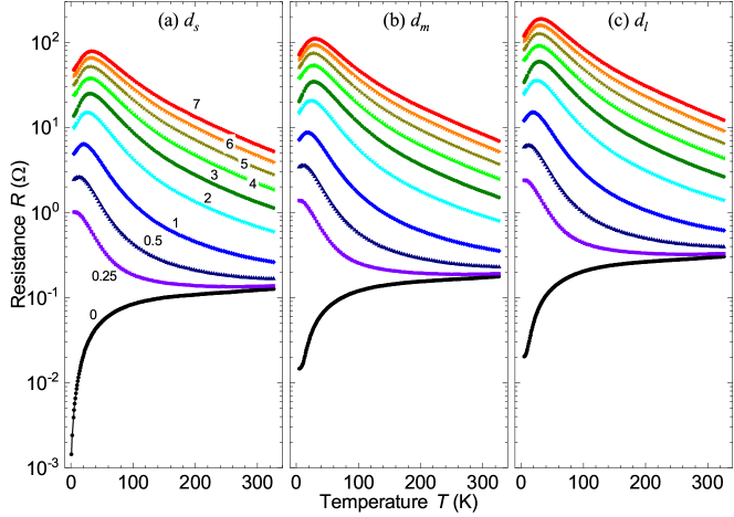
The temperature dependence of the resistance at different constant applied magnetic fields for all three configurations of sample U11 is presented in Figure 5. The typical field-driven metal-insulator transition (MIT) of graphite samples with interfaces is clearly observed .
Magnetoresistance at DC magnetic fields to T
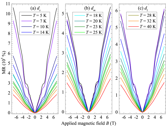
Figure 6 shows the magnetoresistance (MR) at all contacts combinations, , , and at different temperatures. The quantum oscillations, known as Shubnikov-de Haas (SdH) oscillations, are visible at lower temperatures. The SdH oscillations are a signature of the presence of 2D interfaces on a graphite sample.7 Graphite samples without the 2D interfaces show no SdH oscillations. The reason is that the semiconducting crystalline regions have an exponentially small carrier concentration at low temperatures.
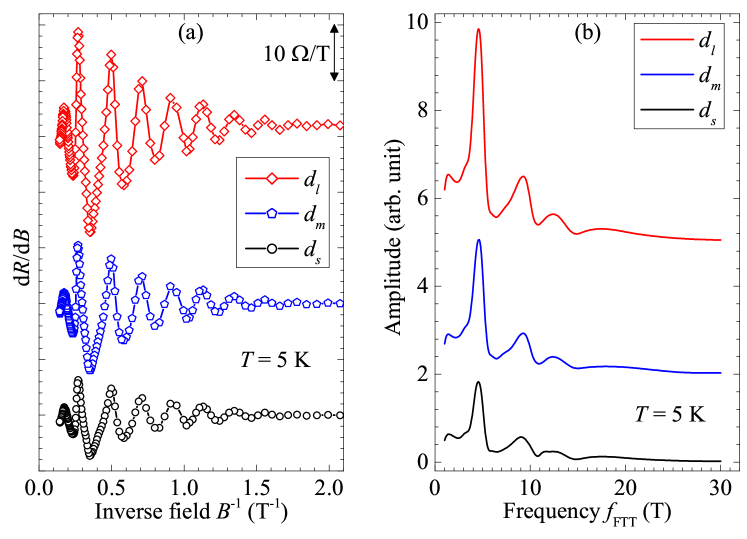
Figure 7 (a) shows the first derivative of the data presented in Figure 6 at K. One can see that the period of the oscillations does not appreciably change with the electrodes locations, only the amplitude of the oscillations changes. For an interpretation of the SdH oscillations in terms of the 2D interfaces and the meaning of the 2D carrier density one obtains from the SdH oscillation frequency we refer to recently published studies.7
Magnetoresistance at pulsed magnetic fields to 65 T
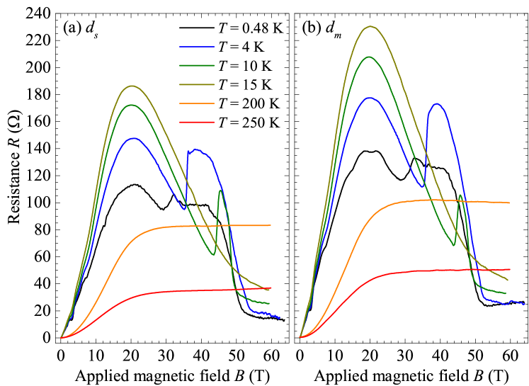
The results of the pulsed magnetic fields applied parallel to the axis at different constant temperatures are shown in Figure 8. Due to difficulties in contacting the sample to perform the measurement simultaneously in all three configurations, we have measured only and . Figure 8 (a) and (b) have the same x- and y-axis scale and they share the same legend. The data showed in Figure 8 was measured simultaneously at each temperature, e.g., one single pulse was used to store the data of the resistance at and .
At K and 200 K the resistance shows a high increase up to 25 T and a weaker increase at higher fields. At K, the resistance reaches a maximum at 21 T and a negative MR at higher fields. Explanations for the change of slope of the MR from positive to negative and the electronic transitions can be found in Ref. 4.
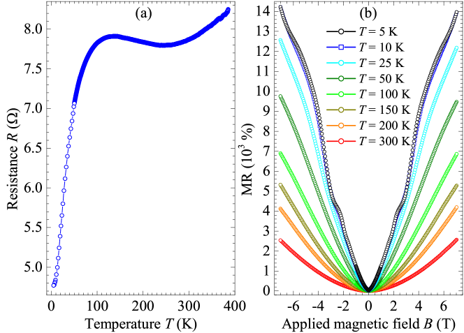
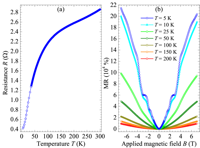
Besides sample U11 we have produced and measured samples U5 and U6 from the same batch of natural graphite from Sri Lanka, using the same technique and placing the contact electrodes also at the edge of these samples. They were characterized at low fields up to T. Measurements at higher field could not be performed because the electrodes burned just before the measurements.
Sample U5
Figure 9(a) shows the temperature dependence of sample U5 of 54 nm thickness. This sample shows a metalliclike behavior from K to 250 K. At lower temperatures to 125 K the resistance increases below K a re-entrance to the metalliclike behavior is observed with a resistance ratio of . Figure 9(b) shows the MR at different constant temperatures.
Sample U6
Figure 10(a) shows the temperature dependence of sample U6 of 114 nm thickness. The temperature dependence shows a metalliclike behavior in all measured range and a ratio of . Figure 10(b) shows the MR at different constant temperatures.
References
- [1] C. E. Precker, P. D. Esquinazi, A. Champi, J. Barzola-Quiquia, M. Zoraghi, S. Muiños-Landin, A. Setzer, W. Böhlmann, D. Spemann, J. Meijer, T. Muenster, O. Baehre, G. Kloess, H. Beth, New J. Phys. 2016, 18, 113041.
- [2] D. Spemann, P. Esquinazi, Evidence for magnetic order in graphite from magnetization and transport measurements, Springer Series in Materials Science 244, P. Esquinazi (ed.), Springer International Publishing AG Switzerland 2016, 45–76.
- [3] D. Spemann, P. Esquinazi, A. Setzer, W. Böhlmann, AIP Advances 2014, 4, 107142.
- [4] J. Barzola-Quiquia, P. D. Esquinazi, C. E. Precker, M. Stiller, M. Zoraghi, T. Förster, T. Herrmannsdörfer, W. A. Coniglio, Phys. Rev. Materials 2019, 3, 054603.
- [5] N. García, P. Esquinazi, J. Barzola-Quiquia, S. Dusari, New Journal of Physics 2012, 14, 053015.
- [6] M. Zoraghi, J. Barzola-Quiquia, M. Stiller, A. Setzer, P. Esquinazi, G. H. Kloess, T. Muenster, T. Lühmann, I. Estrela-Lopis, Physical Review B 2017, 95, 045308.
- [7] M. Zoraghi, J. Barzola-Quiquia, M. Stiller, P. D. Esquinazi, I. Estrela-Lopis, Carbon 2018, 139, 1074.