Wetting of nanopores probed with pressure
Wetting of nanopores probed with pressure
Abstract
Nanopores are both a tool to study single-molecule biophysics and nanoscale ion transport, but also a promising material for desalination or osmotic power generation. Understanding the physics underlying ion transport through nano-sized pores allows better design of porous membrane materials. Material surfaces can present hydrophobicity, a property which can make them prone to formation of surface nanobubbles. Nanobubbles can influence the electrical transport properties of such devices. We demonstrate an approach which uses hydraulic pressure to probe the electrical transport properties of solid state nanopores. We show how pressure can be used to wet pores, and how it allows control over bubbles in the nanometer scale range normally unachievable using only an electrical driving force. Molybdenum disulfide is then used as a typical example of a 2D material on which we demonstrate wetting and bubble induced nonlinear and linear conductance in the regimes typically used with these experiments. We show that by using pressure one can identify and evade wetting artifacts.
I Introduction
A solid state nanopore consists of a solid membrane dividing two solute containers with an opening (pore) with a diameter in the range 1-100 nmDekker (2007). By measuring the changes in the conductance of the sample as a particle passes through the pore opening the particle’s properties, such as size, shape, and charge, can be determined with great accuracy in as low as atto-molar analyte concentrationsWanunu et al. (2010). When the diameter of nanopores is reduced to tens of nanometers and below, they can become selective to ionsVlassiouk et al. (2008) and can provide information on the effective diffusion constants of different ion speciesRollings et al. (2016). Nanopores, and related nanochannels, also enable the study of physical phenomena on the nanoscaleSchoch et al. (2008); Bocquet and Charlaix (2010); Mouterde et al. (2019) and can be used as building blocks for various nanoscale devices which can act as ion pumpsSiwy and Fuliński (2002), electrical diodesSiwy et al. (2005), desalination membranesWerber et al. (2016), or osmotic power generation devicesMacha et al. (2019). Recently, 2D materials like grapheneGaraj et al. (2010); Schneider et al. (2010a); Merchant et al. (2010), hexagonal boron nitride (h-BN)Zhou et al. (2013), and molybdenum disulfide (MoS2)Liu et al. (2014a) have become a popular nanopore membrane because their thickness is comparable to the size of single nucleotides or ions. Due to the ease of nanopore fabrication they are readily used to probe nonlinear ion transport phenomenaJain et al. (2015); Feng et al. (2016); Thiruraman et al. (2018).
Improper wetting and cleaning of nanopore membranes has been connected to an increase in the noise level during ionic current measurementsSmeets et al. (2008); Uram et al. (2008); Beamish et al. (2012). Through localized laser heating it was suggested that bubbles in the nm-size range can remain in nanopores and reduce the conductance of the pores while increasing the electrical noise levelSmeets et al. (2006). Solid-state nanopores have also been used to nucleate nanobubbles through liquid super-heating by large electric fieldsNagashima et al. (2014); Levine et al. (2016) or with plasmonic nanoporesLi et al. (2015). Although bulk gas nanobubbles were identified nearly 20 years agoLou et al. (2000); Ishida et al. (2000), their long term stability on surfaces was a matter of controversy until recentlyAlheshibri et al. (2016). Nanobbubles have been demonstrated to be stable for days or even months on surfaces with receding contact angles larger than or advancing contact angles of or higher (e.g. Mica, HOPG, coated Si)Lohse and Zhang (2015). A hydrophobic surface is defined by a receding contact angle above Law (2014), so even mildly hydrophobic surfaces can support stable surface nanobubbles.
Nanobubbles made from ambient air have been detected on graphene surfaces using transmission electron microscopyShin et al. (2015) and atomic force micrscopyCantley et al. (2019). We expect 2D materials to have two properties which would contribute to the stability of surface nanobubbles: the presence of contaminants during material transferGraf et al. (2019), and an inherently low wettability. 2D materials can have a large variation in the degree of hydrophobicity depending on material type, defect density, and sample quality, with contact angles above reported for MoS2Gaur et al. (2014); Chow et al. (2015); Annamalai et al. (2016), h-BNLi et al. (2017a), and grapheneTaherian et al. (2013); Annamalai et al. (2016). In addition, sample defect density and ambient air exposure has been shown to increase the hydrophobicity of these materials, with fresh samples being more hydrophilicKozbial et al. (2014); Chow et al. (2015). Some of these materials, like h-BNZhou et al. (2013), can be made more hydrophilic by chemical or ozone treatments.
Identifying the presence of nanobubbles and wetting issues on nanopores can be a daunting task. If only ion transport measurements are used, it provides limited information on the nature of the conductance pathway through a pore and needs to be coupled with modeling and prior imaging of pores. Our approach to provide additional information is to use hydraulic pressure as a complementary probe to ionic transport. Hydraulic pressure is known to modify ionic current rectification of nanoporesLan et al. (2011a), and can be used to probe the role of fluid flow in nanopore electrical transportJubin et al. (2018), or fluid flow on the angstrom scaleMouterde et al. (2019). The use of pressure with thin nanopores has mostly been oriented towards influencing DNA or protein translocations Buyukdagli et al. (2015); Li et al. (2017b); Zhang et al. (2018) or for characterising the role of pore surface properties for translocationsFirnkes et al. (2010); Waduge et al. (2017). For ultrathin membrane materials as the ones used in this work, the flow through nanopores is dominated by hydrodynamic access resistance at pore entrancesMao et al. (2014); Gravelle et al. (2014), similar to conductance effects. The nature of the flow lines is that they converge at pore entrances which can drag objects through the poreLan et al. (2011b); Gadaleta et al. (2015). Additionally, hydrostatic pressure has been demonstrated as a way to wet hydrophobic porous materialsSmirnov et al. (2010), an alternative to electrical field induced wettingSmirnov et al. (2011); Powell et al. (2011), but has not yet been demonstrated on single pores.
The aim of this work is to demonstrate that nanoscale bubbles originating from dissolved ambient air in the solutions can significantly modify the measured ionic transport properties of nanopores. First, we will demonstrate the combination of pressure and voltage probes and use it to control the wetting state of a single hydrophobic nanopore. This allows us to establish a baseline of how improper wetting and its effect on ionic conductance of a pore manifests. Secondly, we show how pressure provides a means of identifying and removing nanobubbles or other wetting artifacts in hydrophilic nanopores. Lastly, we will study bubble and wetting induced ionic transport artifacts on MoS2 and demonstrate how alcohol prewetting can grow nanobubbles. Pressure is demonstrated as a viable alternative for wetting and probing the state of nanopores.
II Nanofluidics set-up description
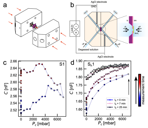
Applying hydrostatic pressure on membranes with nanopores requires water-tight sealing of the sample. This has the added benefit of minimizing water evaporation and gas permeation. To that end, we designed a closed microfluidics chamber made from PEEK and PTFE components which sustain pressures in excess of 10 bar (Fig. 1a). The sample is placed between the two halves of the chamber and sealed using two nitrile O-rings. On each side of the chip there are three fluid pathways: one for an electrode, one for a fluid inlet, and one for a fluid outlet. On both outlets exchange reservoirs are placed onto which compressed gas with pressures up to 7 bar is applied using a microfluidics pressure controller which is also used to measure the applied pressure . The design has minimal crevices and corners to minimize bubble formation during filling of the chambersPereiro et al. (2019). Filling of the chamber is done with solutions which have been degassed from dissolved ambient air in the connecting fluid pathway using a degassing tube. We find that any mixing of the solution or contact with ambient air results in significant gas absorption, regassing the liquids.
By applying a voltage bias between the two Ag/AgCl electrodes on different sides of the membrane we are able to measure current passing through the nanopore (Fig. 1b). In addition, we apply a sinusoidal set voltage (AC) and measure the corresponding current using a phase sensitive amplifier (lock-in). This allows the use of the delay in the AC signal to calculate the capacitance of the membrane. We assume the simplest case of a parallel connection of a capacitance and resistor , where the resistance corresponds to the resistance of the pore as obtained at DC values when the frequency of the AC signal is kept at around 1 Hz (See Supplemental information Sec. S2). In reality the frequency response of a membrane has other contributions but they are only relevant at higher frequenciesDimitrov et al. (2010); Traversi et al. (2013), with a flat plateau at sufficiently low frequencies where measurements are conducted. For 20nm thick suspended silicon nitride membranes in the size ranges of 10x10 to 50x50 m2 which we use here we obtain the expected values for the capacitance on the order of 1 nF (in 1M KCl Tris buffered to pH8)Dimitrov et al. (2010) and proportional to the supported membrane area.
The microfluidics chamber allows the application of hydrostatic pressure in a gradient condition , with a positive pressure gradient defined as pressure applied from the front side of the membrane, and negative from the back side (Fig. 1b). It also allows applying compression pressure on both sides of the membrane simultaneously. Applying pressure on one or both sides of the chip is used as an additional probe of the system. We alternate between no applied pressure and a cycle of pressures going from to , and back down to . In the case that a gradient of pressure is applied, negative pressures are also applied following the same procedure. This allows the detection of any hysteresis in a measured response to the pressure and if the base value at is changing during the measurement. During the pressure cycle either the current response to a bias voltage or the resistance and capacitance using an AC response are measured. The representative value is measured after a sufficient settling time. Examples of applied pressures and measured responses are provided in the Supplemental information.
Compression of solutions, especially degassed ones, has been shown to be comparable in effectiveness to alcohol wettingPereiro et al. (2019). To demonstrate this and to prove proper wetting of membranes, the amount of surface area of the membrane in contact with the liquid is monitored via the membrane capacitance . An example measurement of capacitance for several sweeps of compression pressure is shown on Fig. 1c,d for a hydrophilic (Sample 1) and a hydrophobic surface (Sample 1). As pressure is applied to a freshly degassed solution the baseline value of C, at intermediary steps in the sweep protocol, increases throughout the protocol. In the case of solid state nanopores the largest contribution to the capacitance at low frequencies is known to come from the suspended membrane itselfDimitrov et al. (2010). If part of the suspended membrane with a surface area is not wetted, i.e. there are bubbles or air patches present, then the total capacitance of the membrane will be reduced by an amount (See Supplemental Material Sec. S3 for details). In that sense, the increase of capacitance as pressure is applied is interpreted as the membrane being wetted and gas from the bubbles being absorbed into the liquid which was under-saturated with gas. Hydrophilic membranes fill fast, within tens of seconds of applied compression pressure with a degassed solution, while hydrophobic pores sometimes seem to have remnants of bubbles left on the surface (Fig. 1d. In contrast if a non-degassed solution is used, we report that the capacitance often returns close to its original value, implying that if the solution is saturated excess dissolved gas can return to the membrane in the form of gas bubbles, or that the bubbles are impervious to absorption. In all the following measurements the membranes were flushed with degassed solutions and compression pressures of up to 7 bar were applied for 5 minutes to ensure proper wetting.
III Wetting nanopores coated with hydrophobic polymers
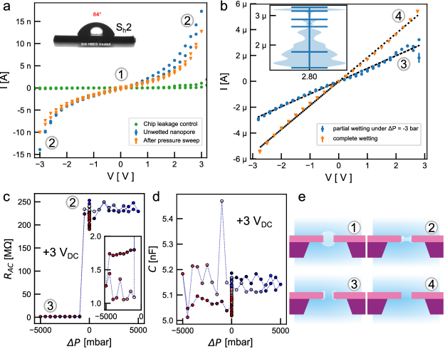
We will first demonstrate how the combination of electrical and pressure probes can be used to wet hydrophobic nanopores. To that end a 130 nm diameter pore in 20 nm thick silicon nitride was coated with a hydrophobic silane hexamethyldisilazane (HMDS) so that we assume that the interior of the pore is also covered. The final static contact angle of was measured by a macroscopic water drop on the chip. The nanopore was wetted using a degassed solution of 1 M KCl Tris buffered to pH8 in the chamber. Fig. 2a shows the measured current versus applied voltage bias through the membrane after wetting for sample Sh2. The measured dependence of current versus applied DC voltage (IV curve) has a characteristic nonlinear shape which is not related to the leakage current through the membrane. Although high voltages can cause pore enlargement or formation, for the material used here the dielectric breakdown voltage is expected to be V but will highly depend on the silicone nitride properties such as defect density.Kwok et al. (2014) To ensure that the measured IV curves are not the result of a leakage current through the membrane, the same measurements on membranes from the same production batch but without any nanopores are performed (Fig. 2a), indicating leakage current is negligible. Wetting curves such as the one in Fig. 2a were obtained in a study on voltage-gating in hydrophobic nanoporesSmirnov et al. (2011), where they were attributed to the electrical field forcing the gas-liquid interface menisci on opposite sides of the membrane to touch through the nanopore. This produces a nonlinear voltage dependent conductance as higher voltages increase the overlap area of the menisci. Applying higher potential differences between the two sides of the nanopore can wet the pore in a process termed electro-wetting even at no applied pressure differenceSmirnov et al. (2011); Beamish et al. (2012, 2012). This state was found to be temporary, reverting to an unwetted state after some time, unless even higher voltages were applied which would drive all the remnants of gas out of the pore area and remove any gas nucleation sites.
In order to transition the sample from its unwetted state in Fig. 2a to a wetted one a combination of pressure gradients and DC voltage bias are applied. After sweeping the applied DC voltage an application of a bar was sufficient to wet the pore (Fig. 2b). Although pressure gradient induced wetting of nanopores was described and measured in porous mediaSmirnov et al. (2010), to our knowledge this is the first instance of pressure induced wetting of a single nanopore. The current baseline of this wetted state was stable except around +3 V of bias which demonstrated fluctuations in the current level. These fluctuations have been detected previously near critical voltages for electrowettingSmirnov et al. (2011), and we attribute them here to partial wetting/de-wetting as already described in both solid state poresSmirnov et al. (2011); Powell et al. (2011) and biological channelsAryal et al. (2015). If a sweep of pressure ( bar 7 bar bar bar) was performed, the state of the pore changed reversibly from the unwetted to the wetted and back to the unwetted state (Fig. 2c). During this pressure sweep there was no significant change of capacitance (Fig. 2d) which we interpret as no large bubbles moving on/off the membrane and changing its capacitance. An IV curve measured after this switching (Fig. 2a) closely matches the IV curve of the original unwetted state. Note that the resistance in the partially wetted state is still larger than the expected resistance for these pores by a factor of two. We interpret this as the pore interior not being completely wetted, in accordance to the scenario proposed that permanent and complete electrowetting is achieved with applying higher voltagesSmirnov et al. (2011). After further application of high voltage and compression pressure the pore was wetted with a resistance of M matching the expected resistance for a nanopore of this size (Fig. 2b). In an ideal case one would expect that both positive and negative pressure should wet the pore, but an asymmetry in the nanopore unwetted volume is attributed to a preference for one direction of the pressure gradient. In conclusion, pressure and electrical potential bias can be used to wet even hydrophobic pores. Attempts to wet smaller coated pores (75 nm) were unsuccessful, consistent with previous studies indicating that even higher critical voltages and pressures would be requiredSmirnov et al. (2011). Sample Sh1 was wetted with compression pressure after several hours of high voltage IV curves, but its coating was less successful with a measured angle of (Supplemental information Sec. S5).
IV Wetting artifacts in hydrophilic pores
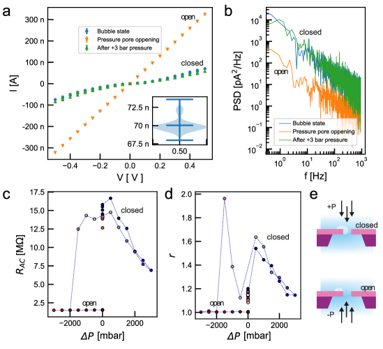
Even with hydrophilic nanopores one can obtain temporary obstructions or other unexpected phenomena which are hard to interpret. In the process of testing our set-up we have found that improper degassing of the solutions in use increases the likelihood of wetting issues. We used fresh oxygen plasma treated silicon nitride pores with a diameter of nm which are standard support membranes for working with 2D materials. It was found that wetting artifacts would be induced at the nanopore under an applied voltage or pressure gradient at the start or during measurements. An example of a measured IV curve we attribute to a nanobubble being pinned at the pore entrance is shown on Fig. 3a. The IV curve presents a nonlinear shape similar to the wetting curve in Fig. 2 albeit with ten times higher currents at the same voltage. It was found that pressure gradients or even higher voltages could be used to change the state of the pore. By sweeping the gradient pressure in the range of bar the state of the pore was changed from a resistive and nonlinear one ( M) to a linear and more conductive one ( M). An IV curve corresponding to this linear and conductive state is shown in Fig. 3a which confirms the stability of such a state for minutes or longer. Then by applying bar for several seconds the resistance is again returned into a similar obstructed state. We argue that the pressure induced fluid flow is moving an object in and out of the pore, partially obstructing it. Any flow through a nanopore will have the flow lines bent and converging towards the pore entrance producing drag forces. The resulting drag force will have components in both the plane of the membrane and in the direction through the pore, which can then cause both translocations and moving of objects closer to the pore center. The difference between hydraulic pressure induced flow and electrical field induced drag (which would also include electroosmotic flowMelnikov et al. (2017)) is in the streamline shape and the magnitude of the drag force. The magnitude of pressure induced drag is proportional to the dimensions of the object while the electric field induced force is additionally dependent on the surface charge.
The reason why the behavior on Fig. 3 is not attributed to a wetting-dewetting transition, but to a nanobubble obstruction, lies in the noise level, the dependence of the resistance on pressure, and the presence of ionic current rectification. The current power spectral density (Fig. 3b) is consistent with previous works predicting that nanobubbles in solid state pores increase the noise levelSmeets et al. (2006). The noise power spectral density at frequencies below several kHz is dominated by flicker noise, which is known to scale with frequency as with and the flicker noise amplitudeTabard-Cossa et al. (2007); Uram et al. (2008); Gravelle et al. (2019). We find the flicker noise level in all the samples presenting bubble issues to be slightly higher than ideal for such samplesTabard-Cossa et al. (2007); Smeets et al. (2008); Uram et al. (2008). It has also been predicted to increase in the case of wetting issuesBeamish et al. (2012). We notice several pressure induced behaviors in our measurements. First, the noise would sometimes increase or decrease after applying a pressure gradient, probably depending on if the pore was wetted or dewetted with the pressure. Secondly, we note that in some cases a decrease of resistance after applying pressure was followed with an increase in flicker noise amplitude. We speculate that the nature of the flicker noise will most likely depend on the surface charge of the air bubble, its shape, and position within the pore. For example if the bubble is changing the resistance dominantly from obstructing the pore channel or the access area to the pore, the contributions to the flicker noise will be differentFragasso et al. (2019), with predictions that the surface contribution is more pronounced than the bulk contribution in nanopores smaller than 20 nm. We conclude that the noise level can strongly vary based on the position and shape of the obstructing bubble, with the lowest possible noise level only achieved once the whole pore region is completely wettedTabard-Cossa et al. (2007); Beamish et al. (2012). The mechanism of bubble pining here is unclear, but from the ease of moving the bubbles between an obstructing and non-obstructing state we postulate that it could be due to small defects or contaminants that survived the sample cleaning procedure. It could also be the fact that the pore is too small to let a bulk nanobubble pass through it.
Fig. 3c shows that in the closed state there is a decrease in resistance of the pore as a pressure gradient is applied from 0 to 3 bar. If the bubble was pinned on the front side of the membrane then once the bubble is inside the pore additional flow from increased pressure gradient would deform and elongate the bubble thus opening up a wider pathway for fluid flow and decreasing the resistance. Something that would not occur in the case of a solid obstruction. We notice that the obstructing object is easily flushed through by a longer and consistent use of higher voltages or pressures in either direction, making it hard to obtain these measurements. Another indicator connected to the presence of nanobubbles in solid state pores is the level of ionic current rectificationLi et al. (2015). Ionic current rectification defined as is known to increase when there is geometrical asymmetry or surface charge asymmetry in nanopores. Since our nanopores are symmetric, an increase in would be an additional indicator of a nanobubble or other obstructing object being present. The values of calculated from the AC response during the pressure sweep are provided in (Fig. 3d). The ionic current rectification increases when the pore is in the obstructed state, and is practically nonexistent in the open state (See supplemental information for details). We performed finite element modeling using coupled Poisson-Nernst-Planck-Stokes equations of four different example static scenarios: a) an open pore, b) a pore with an air bubble next to the pore entrance, c) a pore with an obstructing object clogging the pore, and d) a pore constricted by a symmetric air bubble. In all cases, the change of resistance versus pressure is negligible. Pressure induced flow is found to reduce ionic current rectification in the case of large openings, but not in the case of small pores. This effect has been studied previously and was attributed to flow negating the local charge distribution in the nanopore which is responsible for ionic current rectificationLan et al. (2011a); Jubin et al. (2018).
In conclusion, we find that none of these four static cases can explain such a large change in the resistance R or rectification r versus pressure P (See Supplemental information Sec. S4 for the details), strengthening our hypothesis that flow is inducing a movement or deformation of the obstructing object. In addition, we were not able to obtain the activated non-linear IV curve in these models as seen in the case of the closed state in Fig. 3. Previous works have either attributed this non-linearity to temporary electrowettingSmirnov et al. (2011) or to hydration layer shreddingCantley et al. (2019); Jain et al. (2015). Hydration layer shredding would require that the constriction is comparable to the size of the ions, which is inconsistent with the large variaton of both resistance and rectification with pressure, especially as it is known that pressure does not reduce ionic current rectification for small nanopores due to too low flow ratesLan et al. (2011a). Here we note that surface conduction and not Debye layer overlap is responsible for ionic current rectificationPoggioli et al. (2019), so that due to the nanobubble surface charge the unobstructed area of the pore opening can have larger dimensions than the Debye screening length which is nm in our conditions. We conclude that the presented experimental data supports a dynamic change of the obstructing object at the nanopore which is consistent with bad wetting most likely due to the presence of a bubble in the nanoscale size range.
V Wetting artifacts with 2D materials
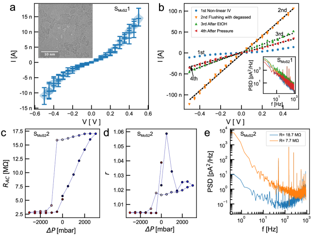
Single layer MoS2 supported on the same 75 nm diameter pores in 20 nm thick silicon nitride as in the previous measurements is used. An example of measurements obtained on a TEM drilled MoS2 nanopore (Sample M1) with several 2 nm pores are shown on Fig. 4. Only degassed solutions of 1M KCl Tris buffered to pH 8 were used and compression pressures of up to 7 bar were applied while filling the nanopore until the measured capacitance of the membrane stabilized. The IV response of the nanopore is shown on Fig. 4a. This IV curve shape was persistent for one day of measurements, with fluctuations in the IV curves initially reducing after several hours and the flicker noise increasing. The evolution of the fluctuations is shown in the Supplemental information Sec. S6. The shape of the IV curve closely matches the wetting curve in Fig. 2a with a non-linear activated behaviour. As the TEM imaged size of the pore is above the size where any hydration layer or single ion effects could take place, we attribute this state to a wetting issue. After flushing with degassed solution the pore exhibited a linear IV curve corresponding to a resistance of M, or a pore in MoS2 of diameter nm (Fig. 4b). Details about MoS2 pore size calculations are provided in the Supplemental information Sec. S2. The pore was then probed with a pressure sweep of bar to test the stability of the pore resistance. The pore resistance was consistent. At this point the influence of using an alcohol wetting technique was investigated. To do so a solvent exchange procedureLou et al. (2000) was performed in which a liquid of higher gas capacity (i.e. alcohol) is exchanged for one of lower gas capacity (i.e. water). A simplified explanation is that in this case the first solvent due to its higher affinity for the hydrophobic surface and higher gas capacity acts as a catalyst for nucleation of gas bubbles. The solution in the chamber was exchanged to 50% ethanol 50% water mix, twenty minutes of equilibration time was allowed followed by an exchange back to degassed 1M KCl Tris buffered to pH8. The solvent exchange procedure increased the resistance of the nanopore to M (calculated pore diameter nm) while retaining a linear IV curve. The flicker noise amplitude remained the same during all these procedures (Fig. 4b inset), but taking into account the empirical von Hooge relationFragasso et al. (2019) implies that the 2nd curve has the lowest noise as it supports the largest current at a fixed potential (lowest resistance), and thus the best wetting. The linearity of the curve is in contrast with previous observations where bubbles were shown to produce rectification of the ionic currentLi et al. (2015). A further application of compression pressure of bar did not change the resistance, but a pressure gradient sweep in the range bar changed the resistance to M or a calculated pore of diameter nm (Fig. 2b, ”After Pressure”). In this case the rectification did not change, as seen in the linearity of the IV curves. Further flushing with degassed solution reduced the resistance to M (close to the value of M for the supporting nanopore of 75 nm) and was accompanied by a large reduction in the noise level at low frequencies. The potential differences applied on the sample never exceeded V as higher voltages can cause an electrochemical induced opening of MoS2 poresFeng et al. (2015). We hypothesize that the MoS2 was punctured from the start or damaged during one of the flushing procedures and that all measurements except the 2nd (after flushing with degassed solution) were of improper wetting of the pore. Notably, the resistance of this pore was changed, with degassed solutions decreasing it and alcohol wetting increasing it, all at a constant level of flicker noise.
Figure 4c shows another MoS2 sample (S2) which was switched between a high ( M, nm) and low ( M, 30 nm) resistance state but with a stable state at no applied pressure ( M at ). In the high resistance and intermediate state the ionic current rectification was increased, indicating as previously the presence of a bubble. A comparison of the noise before any pressure was applied and after pressure sweeps, indicates that the noise level in the system was increased in the low resistance state. In addition, we performed a streaming potential measurement showing stable fluid flow between two sides of the membrane through the pore before and after this pressure dependent switching (See Supporting information Fig. S7). We interpret this as the bubble changing in size or position, and influencing the noise level at low frequencies. This is consistent with the theory of charge binding/debinding at the bubbles surface being responsible for the low frequency flicker noiseGravelle et al. (2019), where changing the amount of surface area exposed to the solution and its properties, e.g. liquid-gas or liquid-solid interface, would change the noise spectrum. Additional data on three more samples is provided in the Supplemental information Sec. S7, out of which two have been imaged prior to measurements. Fluctuations between linear and nonlinear IV curves are found to be common, and a lower level of the noise power spectral density is not a good measure of bubbles being absent. As with the results from the previous section, the flicker noise can be larger in smaller pores. The gradient pressure clearly shows the ability to change the state of the pore, while compression pressure only changes the state of the pore when a freshly degassed solution is used. One could argue that pressure gradients are damaging the MoS2 and opening up pores. The total force applied on the nm diameter exposed MoS2 is nN at bar which is orders of magnitude smaller both than typical forces applied in atomic force microscopy indentation experimentsLiu et al. (2014b), and forces required to delaminate MoS2Lloyd et al. (2017). We also note that the 20 nm thick supporting silicon nitride membrane can break due to applied pressure gradients at 5-7 bar only if the membrane area is larger than 30x30 m2. That being said even if the MoS2 is being enlarged, it does not modify the observations that bubbles are present and can produce both linear and nonlinear IV curves of varying noise levels. The resistance of the pore comes from two series connected termsKowalczyk et al. (2011), one being the resistance of the pore interior and the other from the access area. This access area contribution to the resistance and noise is larger for smaller poresKowalczyk et al. (2011); Fragasso et al. (2019), and we speculate that a bubble obstructing the access area could have a lesser contribution to the noise level than one which has entered the pore interior.
We note that all MoS2 samples presented here show the same pattern. All samples showed apparent resistances at low voltages ( V) indicating either smaller pores than imaged (samples S1, S4) or pores in materials which were known to have no pores (S3). One could naively use this resistance value to infer nanopores in the 1 nm range if only ionic current measurements were used. At higher voltages they present nonlinear conductivity with the same pattern as seen in the wetting of hydrophobic pores (Fig. 3). This nonlinear conductivity disappears after flushing with degassed solution and compressing with pressure. The resistance of the pores can be reduced by applying negative pressure inducing fluid flow from the back side to the front side of the membrane, and increased by applying positive pressure. This is consistent with the bubble being present on the side of the membrane onto which MoS2 was transferred, as negative pressure (from the back side) would then move the bubble away from the pore opening. A recent study on nanopores in supported graphene using atomic force microscopy demonstrated that bubbles in the 100 nm size range are common and can increase the resistance of the pore and provide a nonlinear signalCantley et al. (2019), which we interpret as wetting issues similar to the non linear curves obtained in Fig. 3, 2 and 4b. The explanation given for this process is that it stems from the use of solvent exchanges from alcohol to aqueous salt solutions, identical to the procedures performed in this study to increase the resistance of the MoS2 pore (Fig. 4b). We conclude by induction that the most probable explanation of such effects is the presence of a bubble in the nm-size range at the nanopore entrance with the supported MoS2 being damaged either before or during wetting.
The possible causes for nanobubbles being stable on the 2D material surface remain to be explained. It is clear that a basic requirement is that the surface of the material be at least mildly hydrophobicLohse and Zhang (2015). 2D materials like graphene, MoS2, h-BN have contact angles which can be larger than the minimum reported for generation of stable nanobubbles on surfaces. This will highly vary on the sample quality and type of supporting surfaceGaur et al. (2014); Chow et al. (2015); Annamalai et al. (2016); Lohse and Zhang (2015). Nanobubbles have been directly visualized so far only on grapheneShin et al. (2015); Cantley et al. (2019). Another possibility is contact line pinning of the nanobubble to the surface via any surface defects or contaminants which have been shown to stabilize the bubbles and aid growthLohse and Zhang (2015); Fang et al. (2016). Contaminants on 2D material surfaces are a common occurrence in typical methods of transfer from growth to supporting surfaces which involve the use of some form of polymer based stampSchneider et al. (2010b); Castellanos-Gomez et al. (2014); Zomer et al. (2011); Graf et al. (2019). The degree of contaminants has been reported to be significantly reduced if a polymer-free transfer method is usedZhang et al. (2016). Usually polymers used for transfer involve PMMA or hydrophobic PDMSBhattacharya et al. (2005). In the case of PMMA, while a homogeneously smooth coating is not expected to support nanobubble pining, patches are expected toAgrawal et al. (2005). The MoS2 samples in this study used a PMMA stamp based transfer method which is known to leave hydrocarbon residuesGraf et al. (2019). This is also confirmed by electron micrographs of the samples (TEM images of three MoS2 samples provided in the Supplemental information). Nanobubble nucleation at surfaces has been shown to be possible even at low levels of overgassing (100-120%) with a temperature change of a few degrees around room temperature inhibiting or promoting nanobubble formationSeddon et al. (2011). The presence of nano-pits or crevices has been found to increase nanobubble stabilityGuo et al. (2016); Wang et al. (2017), large holes in supported 2D membranes would play this role in the nanopore system. The mechanism of nanobubble nucleation and stability on 2D materials is something which would require further study.
VI Conclusions
We show a variety of ionic transport phenomena induced by bubbles or contaminants, and provided a way to control them by using hydraulic pressure gradients between the two sides of a nanopore. This has allowed us to shed light on an important concept for the 2D nanopore community: how hydrophobicity and nanoscale defects or contaminants can enable improper wetting or nanobubbles to imitate other effects. Samples which would normally either be misinterpreted or rejected are found to be plagued by wetting issues. One of the reasons for these wetting issues with 2D materials is the use of alcohol prewetting, a technique prevalent in the solid state nanopore communityJain et al. (2015); Feng et al. (2016); Heerema et al. (2018); Graf et al. (2019). This part of a nanopore filling protocol, if combined with hydrophobic or contaminated surfaces, is equivalent to the standard technique of solvent exchange used to nucleate nanobubbles on hydrophobic surfacesLohse and Zhang (2015). We believe that this protocol was carelessly transferred from its use with hydrophilic pore materials to hydrophobic and contaminated 2D materials. The standard methods of wetting hydrophobic pores which involve high voltagesBeamish et al. (2012); Smirnov et al. (2011) would damage the material by producing and enlarging surface defects via electrochemical reactionsFeng et al. (2015); Kuan et al. (2015). In this context, we demonstrate that the combination of degassing and applying pressure in a closed air-tight chamber is a suitable method for wetting. Even in the case where complete wetting is not possible due to stability of nanobubbles in degassed solutionsQian et al. (2019), pressure induced fluid flow has been demonstrated as a useful tool to detect and possibly remove nanobubbles and other contaminants. This is especially relevant in cases where wetting issues reduce an already low yield with complex fabrication protocols, for example the addition of transverse electrodes for DNA translocationsHeerema et al. (2018). DNA translocations have been used as an argument for proper wetting if the current drops match the expected size of the nanopore. If the current drop of the translocating molecule corresponds to the size of the pore it can be a good indicator of proper pore wetting but if it deviates one should consider among other factors also improper wetting of the pores. A suitable alternative to DNA translocations could be found in streaming measurementsFirnkes et al. (2010); Waduge et al. (2017). Streaming is a natural extension to the method presented here and can be performed in situ with no modifications to the experimental setup, as demonstrated for the case of MoS2.
Wetting is especially problematic if combined with the study of 1 nm sized pores in 2D materials, which are expected to have resistances comparable to electrowetting curves of hydrophobic pores at small applied voltagesSmirnov et al. (2011). In the future additional proof needs to be provided of proper wetting of nanopores in 2D materials to corroborate claims of any finite size ion or nonlinear effectsJain et al. (2015); Feng et al. (2016) as our work shows that the shape of IV curves can be considerably modified by bubbles and/or unwetted pores which are stable for more than several hours. We have demonstrated that using pressure induced fluid flow can modulate the apparent resistance of a nanopore by moving or changing the size and shape of a pinned gas bubble, but the same approach is also valid for any type of solid obstruction at the pore entrance. Both linear and nonlinear IV curves in the range of V can be obtained in this way. We also find that the noise level can be reduced by applying pressure as expected by improved wettingBeamish et al. (2012), but also that it is possible to obtain relative increases in low-frequency noise when the resistance of the pore is increased. The exact geometry, shape, and size of nanobubbles can influence the level of noise at low frequenciesFragasso et al. (2019); Gravelle et al. (2019), so we argue it will be hard to judge if slight variations in the noise are indicative of the removal of nanobubbles as was previously expectedSmeets et al. (2006); Uram et al. (2008); Beamish et al. (2012). We do notice the presence of current fluctuations between two or more states as reported in works on hydrophobic pores and connected to a wetting/dewetting transitionSmirnov et al. (2011); Powell et al. (2011) which is also indicative of the presence of bubbles.
The existence of even the slightest level of ionic current rectification can be an indicator of bad wetting which can modify the resistance of the nanopore. Standard DC methods in use will not always be sufficient. The best approach is to combine this with an in situ probe, like laser light irradiationSmeets et al. (2006) or as demonstrated in our case hydrostatic pressure. Also, as we have seen wetting issues can relax over the time scale of hours, indicating that experiments should be done for longer times using a sealed sample chamber to prove nanopore stability. And in the case of any potentially contaminated and hydrophobic materials (e.g. 2D materials), the technique of solvent exchange should be used with care and preferentially only degassed solutions used.
VII Methods
VII.1 Microfluidics chamber
The microfludic flow-cell was designed to accommodate 5x5mm Si/SiN membrane devices under high working pressure and closed salt solution circulation providing precise pressure control, electrical and thermal insulation. All flow-cell components in contact with the fluid are made from polyether ether ketone (PEEK). Fluid connections to the flow-cell are made with PTFE tubing and connections made with HPLC grade ferrules and fittings. The fluidic pathways are sealed with mechanical shut-off valves. All liquid exchanges are done by flushing liquid through these fluidic connections using Luer-lock syringes. Liquids are degassed by pushing the fluid first through a 4 ml internal volume degassing hose (Biotech Fluidics BT-9000-1549) connected to a vacuum pump at 10 mBar absolute vacuum. Nitrile O-rings were used to ensure sealing of the chip between the two halves of the chamber. The internal volume of each side of the chamber is ml so we always performed exchanges of solutions by flushing at least mL of liquid trough each side of the chamber, with added pauses to ensure proper mixing even in dead areas without flow. The flow-cell was cleaned by 20 min sonnication in 70∘C MiliQ water (18.2 M/cm, 200 nm filtered) to dissolve any remnant salt crystals, then for 20 minutes by sonnicating in isopropanol to remove any greasy residues, then for at least two 20 min sonnications in MiliQ water before drying overnight at 70∘C. The chamber and the O-rings were treated with oxygen plasma for 30s to make the surface hydrophilic prior to use. Chlorinated Ag/Cl electrodes were sealed using the same fittings and ferrules as the connecting tubing. To ensure there are no air pockets near the electrodes they were partially unscrewed and liquid in the chamber was used to push any air out.
VII.2 Measurements
All electrical measurements were done using a Zurich Instruments MFLI lock-in amplifier with the MF-DIG option. Both DC and AC bias was applied using the signal output of the instrument, while the current through the sample was measured using the built in current to voltage converter. All DC (AC demodulator) signals were sampled at 1.83 kHz (1.6 kHz) and acquired using the MFLI lock-in amplifer. The input noise used by the amplifier depended on the current input range used and was generally bellow 200 fA. All measurements were done inside a Faraday cage. Note that the presence of mains line noise in some of the current spectral power densities was because a short coaxial cable was used between the Faraday cage and MFLI instrument, which coupled with the connection for signal output from the lock-in produced a ground loop. All DC IV curves were recorded in a sweep from to , down to and back to to ensure any hysteresis is visible. Thus, for all set voltage values, except the highest and lowest, two points are shown on all figures. Pressure was applied and controlled with % nitrogen using a 7 bar FlowEZ microfluidics pressure controller (Flugient). All interfacing with the measurement instruments was done using a custom made program in LabVIEW. All measurement data was analysed using a custom made script in Python using SciPy signal analysis toolsVirtanen et al. (2019).
All electrical measurements performed while sweeping the pressure were done after the pressure level has stabilized to at least 5% of the target value. In the case of DC current measurements an additional wait time of 1 s was performed after the pressure settling. In the case of lock-in measurements the wait time was 15 times the lock-in base time plus 2.5 s. The base time constant used was usually 300ms to 1s for an AC signal at 1 Hz, which was a compromise between the speed of measurements and measurement precision. Pressure measurements and electrical measurements were synchronized only within s which was taken into account during the analysis. Details on the conversion of raw data to resistance and capacitance , the calculation of the AC rectification factor , as well as the measurement protocol are provided in the SI Sec. S2.
We used 1M KCl with 10 mM Tris buffered to pH 8 for all conductance measurements. All buffers were prepared using MiliQ grade water(18.2 M/cm). The conductivity of all solutions was checked before use with a Mettler-Toledo FiveEasy Plus. For solvent exchange we used a 50%/50% mixture of Ethanol and MiliQ water with a measured conductivity of 10 S/cm. All solutions were filtered through a 20 nm filter before use (Whatman Anotop 25 plus).
VII.3 Supporting membranes and MoS2
All the measurements provided in the main text were done using in-house fabricated 20 nm thick silicon nitride membranes based on wafers bought from the same supplier. Two additional controls are provided in the SI using commercially bought membranes from NORCADA. Details of the fabrication procedure and samples are provided in Supplemental information Sec. S1.
MoS2 was synthesized using a modified growth protocol based on growth promoter spincoatingCun et al. (2019). An annealed c-sapphire 2inch wafer was cleaned in IPA/DI and spincoated with sodium molybdate/sodium chloride water mixture (at concentration of 0.03M/0.1M), inserted in the middle of homemade MOCVD hotwall tube furnace and ramped up to 850C under the flow of 210sccm of pure Ar (99.999%) and ambient pressure. During the growth step, metalorganic precursor (MoCO6, Sigma Aldrich 99.9%) and diethyl sulphide (C2H6S2, Sigma Aldrich 98.0%) were supplied from separate bubblers (both at 17C) by an Ar flow of 12 sccm and 3 sccm respectively as well as 4 sccm of H2 and 1 sccm of O2 to improve precursor decomposition, prohibit C contamination and increase the growth yield and quality. After 30min reaction gases were closed and reactor was cooled down naturally. 2D material was transferred to a device using a PMMA based transfer methods reported elsewhereGraf et al. (2019). MoS2 was imaged and drilled using a FEI TEM Talos with an 80kV electron beam in HRTEM mode. Details are provided in the Supplemental information Sec. S1.
VII.4 Supplemental information
Description of samples used along with supplemental measurements from a total of four hydrophilic nanopores (S1, S2, S3, S4) and five MoS2 devices (S1, S2, S3, S4, S5). Description of DC and AC measurements and a discussion of the influence of wetting on the apparent capacitance . A FEM model using coupled Poisson-Nernst-Planck-Stokes equations of the possible scenarios of pore obstruction. An example of a full time trace of an AC pressure sweep.
Author contributions
S.M. designed and built the experimental set-up and designed the study. M.M designed the microfluidic chamber. S.M. and M.M. performed the experiments. A.C. fabricated the devices, transferred and prepared MoS2 devices. M.M. grew the MoS2. A.R. initiated and supervised the research. S.M. analyzed the data, made the FEM model and wrote the manuscript. All authors provided important suggestions for the experiments, discussed the results, and contributed to the manuscript.
acknowledgement
The authors thank J. Gundlach, M. Wanunu, M. Graf, M. Lihter and M. Thakur for useful discussions. This work was financially supported by the Swiss National Science Foundation (SNSF) Consolidator grant (BIONIC BSCGI0_157802) and from the European Union’s Horizon 2020 research and innovation programme under the Marie Skłodowska-Curie grant agreement No 754462.
References
- Dekker (2007) C. Dekker, Nat. Nanotechnol. 2, 209 (2007).
- Wanunu et al. (2010) M. Wanunu, W. Morrison, Y. Rabin, A. Y. Grosberg, and A. Meller, Nat. Nanotechnol. 5, 160 (2010).
- Vlassiouk et al. (2008) I. Vlassiouk, S. Smirnov, and Z. Siwy, Nano Lett. 8, 1978 (2008).
- Rollings et al. (2016) R. C. Rollings, A. T. Kuan, and J. A. Golovchenko, Nat. Commun. 7, 1 (2016).
- Schoch et al. (2008) R. B. Schoch, J. Han, and P. Renaud, Rev. Mod. Phys. 80, 839 (2008).
- Bocquet and Charlaix (2010) L. Bocquet and E. Charlaix, Chem. Soc. Rev. 39, 1073 (2010), arXiv:0909.0628 .
- Mouterde et al. (2019) T. Mouterde, A. Keerthi, A. R. Poggioli, S. A. Dar, A. Siria, A. K. Geim, L. Bocquet, and B. Radha, Nature 567, 87 (2019).
- Siwy and Fuliński (2002) Z. Siwy and A. Fuliński, Phys. Rev. Lett. 89, 4 (2002).
- Siwy et al. (2005) Z. Siwy, I. D. Kosińska, A. Fuliński, and C. R. Martin, Phys. Rev. Lett. 94, 048102 (2005).
- Werber et al. (2016) J. R. Werber, C. O. Osuji, and M. Elimelech, Nat. Rev. Mater. 1 (2016), 10.1038/natrevmats.2016.18.
- Macha et al. (2019) M. Macha, S. Marion, V. V. R. Nandigana, and A. Radenovic, Nat. Rev. Mater. 4, 588 (2019).
- Garaj et al. (2010) S. Garaj, W. Hubbard, a. Reina, J. Kong, D. Branton, and J. a. Golovchenko, Nature 467, 190 (2010), arXiv:1006.3518 .
- Schneider et al. (2010a) G. F. Schneider, S. W. Kowalczyk, V. E. Calado, G. Pandraud, H. W. Zandbergen, L. M. Vandersypen, and C. Dekker, Nano Lett. 10, 3163 (2010a).
- Merchant et al. (2010) C. A. Merchant, K. Healy, M. Wanunu, V. Ray, N. Peterman, J. Bartel, M. D. Fischbein, K. Venta, Z. Luo, A. T. C. Johnson, and M. Drndic, Nano Lett. 10, 2915 (2010), arXiv:1005.4754 .
- Zhou et al. (2013) Z. Zhou, Y. Hu, H. Wang, Z. Xu, W. Wang, X. Bai, X. Shan, and X. Lu, Sci. Rep. 3, 1 (2013).
- Liu et al. (2014a) K. Liu, J. Feng, A. Kis, and A. Radenovic, ACS Nano 8, 2504 (2014a).
- Jain et al. (2015) T. Jain, B. C. Rasera, R. J. S. Guerrero, M. S. H. Boutilier, S. C. O’Hern, J.-C. Idrobo, and R. Karnik, Nat. Nanotechnol. 10, 1053 (2015).
- Feng et al. (2016) J. Feng, K. Liu, M. Graf, D. Dumcenco, A. Kis, M. Di Ventra, and A. Radenovic, Nat. Mater. 15, 850 (2016).
- Thiruraman et al. (2018) J. P. Thiruraman, K. Fujisawa, G. Danda, P. M. Das, T. Zhang, A. Bolotsky, N. Perea-López, A. Nicolaï, P. Senet, M. Terrones, and M. Drndić, Nano Lett. (2018), 10.1021/acs.nanolett.7b04526.
- Smeets et al. (2008) R. M. Smeets, U. F. Keyser, N. H. Dekker, and C. Dekker, Proc. Natl. Acad. Sci. U. S. A. 105, 417 (2008).
- Uram et al. (2008) J. D. Uram, K. Ke, and M. L. Mayer, ACS Nano 2, 857 (2008).
- Beamish et al. (2012) E. Beamish, H. Kwok, V. Tabard-Cossa, and M. Godin, Nanotechnology 23, 405301 (2012).
- Smeets et al. (2006) R. M. Smeets, U. F. Keyser, M. Y. Wu, N. H. Dekker, and C. Dekker, Phys. Rev. Lett. 97, 1 (2006).
- Nagashima et al. (2014) G. Nagashima, E. V. Levine, D. P. Hoogerheide, M. M. Burns, and J. A. Golovchenko, Phys. Rev. Lett. 113, 024506 (2014).
- Levine et al. (2016) E. V. Levine, M. M. Burns, and J. A. Golovchenko, Phys. Rev. E 93, 013124 (2016).
- Li et al. (2015) Y. Li, F. Nicoli, C. Chen, L. Lagae, G. Groeseneken, T. Stakenborg, H. W. Zandbergen, C. Dekker, P. Van Dorpe, and M. P. Jonsson, Nano Lett. 15, 776 (2015).
- Lou et al. (2000) S. T. Lou, Z. Q. Ouyang, Y. Zhang, X. J. Li, J. Hu, M. Q. Li, and F. J. Yang, J. Vac. Sci. Technol. B Microelectron. Nanom. Struct. 18, 2573 (2000).
- Ishida et al. (2000) N. Ishida, T. Inoue, M. Miyahara, and K. Higashitani, Langmuir 16, 6377 (2000).
- Alheshibri et al. (2016) M. Alheshibri, J. Qian, M. Jehannin, and V. S. J. Craig, Langmuir 32, 11086 (2016).
- Lohse and Zhang (2015) D. Lohse and X. Zhang, Rev. Mod. Phys. 87, 981 (2015).
- Law (2014) K.-Y. Law, J. Phys. Chem. Lett. 5, 686 (2014).
- Shin et al. (2015) D. Shin, J. B. Park, Y. J. Kim, S. J. Kim, J. H. Kang, B. Lee, S. P. Cho, B. H. Hong, and K. S. Novoselov, Nat. Commun. 6, 1 (2015).
- Cantley et al. (2019) L. Cantley, J. L. Swett, D. Lloyd, D. A. Cullen, K. Zhou, P. V. Bedworth, S. Heise, A. J. Rondinone, Z. Xu, S. Sinton, and J. S. Bunch, Nanoscale 11, 9856 (2019).
- Graf et al. (2019) M. Graf, M. Lihter, M. Thakur, V. Georgiou, J. Topolancik, B. R. Ilic, K. Liu, J. Feng, Y. Astier, and A. Radenovic, Nat. Protoc. 14, 1130 (2019).
- Gaur et al. (2014) A. P. S. Gaur, S. Sahoo, M. Ahmadi, S. P. Dash, M. J. F. Guinel, and R. S. Katiyar, Nano Lett. 14, 4314 (2014).
- Chow et al. (2015) P. K. Chow, E. Singh, B. C. Viana, J. Gao, J. Luo, J. Li, Z. Lin, A. L. Elías, Y. Shi, Z. Wang, M. Terrones, and N. Koratkar, ACS Nano 9, 3023 (2015).
- Annamalai et al. (2016) M. Annamalai, K. Gopinadhan, S. A. Han, S. Saha, H. J. Park, E. B. Cho, B. Kumar, A. Patra, S. W. Kim, and T. Venkatesan, Nanoscale 8, 5764 (2016).
- Li et al. (2017a) X. Li, H. Qiu, X. Liu, J. Yin, and W. Guo, Adv. Funct. Mater. 27, 1603181 (2017a).
- Taherian et al. (2013) F. Taherian, V. Marcon, N. F. Van Der Vegt, and F. Leroy, Langmuir 29, 1457 (2013).
- Kozbial et al. (2014) A. Kozbial, Z. Li, C. Conaway, R. McGinley, S. Dhingra, V. Vahdat, F. Zhou, B. Durso, H. Liu, and L. Li, Langmuir 30, 8598 (2014).
- Lan et al. (2011a) W.-J. Lan, D. A. Holden, and H. S. White, J. Am. Chem. Soc. 133, 13300 (2011a).
- Jubin et al. (2018) L. Jubin, A. Poggioli, A. Siria, and L. Bocquet, Proc. Natl. Acad. Sci. 115, 4063 (2018).
- Buyukdagli et al. (2015) S. Buyukdagli, R. Blossey, and T. Ala-Nissila, Phys. Rev. Lett. 114, 088303 (2015).
- Li et al. (2017b) J. Li, R. Hu, X. Li, X. Tong, D. Yu, and Q. Zhao, Electrophoresis 38, 1130 (2017b).
- Zhang et al. (2018) H. Zhang, Q. Chen, Y. Wu, Y. Wang, X. Bei, and L. Xiao, Nanotechnology 29, 495501 (2018).
- Firnkes et al. (2010) M. Firnkes, D. Pedone, J. Knezevic, M. Doblinger, and U. Rant, Nano Lett. 10, 2162 (2010).
- Waduge et al. (2017) P. Waduge, R. Hu, P. Bandarkar, H. Yamazaki, B. Cressiot, Q. Zhao, P. C. Whitford, and M. Wanunu, ACS Nano 11, 5706 (2017).
- Mao et al. (2014) M. Mao, J. D. Sherwood, and S. Ghosal, J. Fluid Mech. 749, 167 (2014), arXiv:1405.3583 .
- Gravelle et al. (2014) S. Gravelle, L. Joly, C. Ybert, and L. Bocquet, J. Chem. Phys. 141, 18C526 (2014), arXiv:1501.01476 .
- Lan et al. (2011b) W.-J. Lan, D. A. Holden, J. Liu, and H. S. White, J. Phys. Chem. C 115, 18445 (2011b).
- Gadaleta et al. (2015) A. Gadaleta, A.-l. Biance, A. Siria, and L. Bocquet, Nanoscale 7, 7965 (2015).
- Smirnov et al. (2010) S. Smirnov, I. Vlassiouk, P. Takmakov, and F. Rios, ACS Nano 4, 5069 (2010).
- Smirnov et al. (2011) S. N. Smirnov, I. V. Vlassiouk, and N. V. Lavrik, ACS Nano 5, 7453 (2011).
- Powell et al. (2011) M. R. Powell, L. Cleary, M. Davenport, K. J. Shea, and Z. S. Siwy, Nat. Nanotechnol. 6, 798 (2011).
- Pereiro et al. (2019) I. Pereiro, A. Fomitcheva Khartchenko, L. Petrini, and G. V. Kaigala, Lab Chip 19, 2296 (2019).
- Dimitrov et al. (2010) V. Dimitrov, U. Mirsaidov, D. Wang, T. Sorsch, W. Mansfield, J. Miner, F. Klemens, R. Cirelli, S. Yemenicioglu, and G. Timp, Nanotechnology 21, 065502 (2010).
- Traversi et al. (2013) F. Traversi, C. Raillon, S. M. Benameur, K. Liu, S. Khlybov, M. Tosun, D. Krasnozhon, A. Kis, and A. Radenovic, Nat. Nanotechnol. 8, 939 (2013).
- Kwok et al. (2014) H. Kwok, K. Briggs, and V. Tabard-Cossa, PLoS One 9, e92880 (2014).
- Aryal et al. (2015) P. Aryal, M. S. Sansom, and S. J. Tucker, J. Mol. Biol. 427, 121 (2015).
- Melnikov et al. (2017) D. V. Melnikov, Z. K. Hulings, and M. E. Gracheva, Phys. Rev. E 95, 1 (2017).
- Tabard-Cossa et al. (2007) V. Tabard-Cossa, D. Trivedi, M. Wiggin, N. N. Jetha, and A. Marziali, Nanotechnology 18 (2007), 10.1088/0957-4484/18/30/305505.
- Gravelle et al. (2019) S. Gravelle, R. R. Netz, and L. Bocquet, Nano Lett. 19, 7265 (2019).
- Fragasso et al. (2019) A. Fragasso, S. Pud, and C. Dekker, Nanotechnology 30, 395202 (2019).
- Poggioli et al. (2019) A. R. Poggioli, A. Siria, and L. Bocquet, J. Phys. Chem. B 123, 1171 (2019).
- Feng et al. (2015) J. Feng, K. Liu, M. Graf, M. Lihter, R. D. Bulushev, D. Dumcenco, D. T. L. Alexander, D. Krasnozhon, T. Vuletic, A. Kis, and A. Radenovic, Nano Lett. 15, 3431 (2015), arXiv:1504.04962 .
- Liu et al. (2014b) K. Liu, Q. Yan, M. Chen, W. Fan, Y. Sun, J. Suh, D. Fu, S. Lee, J. Zhou, S. Tongay, J. Ji, J. B. Neaton, and J. Wu, Nano Lett. 14, 5097 (2014b).
- Lloyd et al. (2017) D. Lloyd, X. Liu, N. Boddeti, L. Cantley, R. Long, M. L. Dunn, and J. S. Bunch, Nano Lett. 17, 5329 (2017).
- Kowalczyk et al. (2011) S. W. Kowalczyk, A. Y. Grosberg, Y. Rabin, and C. Dekker, Nanotechnology 22, 315101 (2011).
- Fang et al. (2016) C. K. Fang, H. C. Ko, C. W. Yang, Y. H. Lu, and I. S. Hwang, Sci. Rep. 6, 1 (2016).
- Schneider et al. (2010b) G. F. Schneider, V. E. Calado, H. Zandbergen, L. M. Vandersypen, and C. Dekker, Nano Lett. 10, 1912 (2010b).
- Castellanos-Gomez et al. (2014) A. Castellanos-Gomez, M. Buscema, R. Molenaar, V. Singh, L. Janssen, H. S. J. van der Zant, and G. A. Steele, 2D Mater. 1, 011002 (2014), arXiv:1311.4829 .
- Zomer et al. (2011) P. J. Zomer, S. P. Dash, N. Tombros, and B. J. Van Wees, Appl. Phys. Lett. 99, 5 (2011), arXiv:1110.1045 .
- Zhang et al. (2016) G. Zhang, A. G. Güell, P. M. Kirkman, R. A. Lazenby, T. S. Miller, and P. R. Unwin, ACS Appl. Mater. Interfaces 8, 8008 (2016).
- Bhattacharya et al. (2005) S. Bhattacharya, A. Datta, J. M. Berg, and S. Gangopadhyay, J. Microelectromechanical Syst. 14, 590 (2005).
- Agrawal et al. (2005) A. Agrawal, J. Park, D. Y. Ryu, P. T. Hammond, T. P. Russell, and G. H. McKinley, Nano Lett. 5, 1751 (2005).
- Seddon et al. (2011) J. R. Seddon, E. S. Kooij, B. Poelsema, H. J. Zandvliet, and D. Lohse, Phys. Rev. Lett. 106, 19 (2011), arXiv:1011.1786 .
- Guo et al. (2016) Z. Guo, Y. Liu, Q. Xiao, and X. Zhang, Langmuir 32, 11328 (2016).
- Wang et al. (2017) Y. Wang, X. Li, S. Ren, H. Tedros Alem, L. Yang, and D. Lohse, Soft Matter 13, 5381 (2017).
- Heerema et al. (2018) S. J. Heerema, L. Vicarelli, S. Pud, R. N. Schouten, H. W. Zandbergen, and C. Dekker, ACS Nano 12, 2623 (2018).
- Kuan et al. (2015) A. T. Kuan, B. Lu, P. Xie, T. Szalay, and J. A. Golovchenko, Appl. Phys. Lett. 106, 203109 (2015).
- Qian et al. (2019) J. Qian, V. S. Craig, and M. Jehannin, Langmuir 35, 718 (2019).
- Virtanen et al. (2019) P. Virtanen, R. Gommers, T. E. Oliphant, M. Haberland, T. Reddy, D. Cournapeau, E. Burovski, P. Peterson, W. Weckesser, J. Bright, S. J. van der Walt, M. Brett, J. Wilson, K. Jarrod Millman, N. Mayorov, A. R. Nelson, E. Jones, R. Kern, E. Larson, C. J. Carey, b. Polat, Y. Feng, E. W. Moore, J. Vand erPlas, D. Laxalde, J. Perktold, R. Cimrman, I. Henriksen, E. Quintero, C. R. Harris, A. M. Archibald, A. H. Ribeiro, F. Pedregosa, P. van Mulbregt, and S. . . Contributors, arXiv e-prints , arXiv:1907.10121 (2019), arXiv:1907.10121 [cs.MS] .
- Cun et al. (2019) H. Cun, M. Macha, H. Kim, K. Liu, Y. Zhao, T. LaGrange, A. Kis, and A. Radenovic, Nano Res. 12, 2646 (2019).