Detection of Fermi Arcs in Weyl Semimetals through Surface Negative Refraction
Abstract
One of the main features of Weyl semimetals is the existence of Fermi arc surface states at their surface, which cannot be realized in pure two-dimensional systems in the absence of many-body interactions. Due to the gapless bulk of the semimetal, it is, however, challenging to observe clear signatures from the Fermi arc surface states. Here, we propose to detect such novel surface states via perfect negative refraction that occurs between two adjacent open surfaces with properly orientated Fermi arcs. Specifically, this phenomenon visibly manifests in non-local transport measurement, where the negative refraction generates a return peak in the real-space conductance. This provides a unique signature of the Fermi arc surface states. We discuss the appearance of this peak both in inversion and time-reversal symmetric Weyl semimetals, where the latter exhibits conductance oscillations due to multiple negative refraction scattering events.
I introduction
In recent years, the classification of topological phases of matter has been extended from topological insulators Hasan and Kane (2010); Qi and Zhang (2011) to topological semimetals Armitage et al. (2018); Fang et al. (2016). The latter involves gapless band structures with nontrivial topological properties. Depending on whether the gap closing occurs at isolated points in the Brillouin zone or along closed loops, they are mainly divided into Weyl/Dirac semimetals Wan et al. (2011); Murakami (2007); Burkov and Balents (2011); Wang et al. (2013); Weng et al. (2015); Huang et al. (2015) and nodal-line semimetals Burkov et al. (2011). The unique topological properties of these gapless band structures are extensively explored using a wide variety of platforms, including solid state materials Wan et al. (2011); Murakami (2007); Burkov and Balents (2011); Wang et al. (2013); Weng et al. (2015); Huang et al. (2015); Lv et al. (2015a); Xu et al. (2015a, b, c, 2016); Deng et al. (2016); Yang et al. (2015); Huang et al. (2016); Tamai et al. (2016); Jiang et al. (2017); Belopolski et al. (2016); Lv et al. (2015b); Chen et al. (2018); Chen and Lado (2019), but also using photonic Lu et al. (2013, 2015), phononic Xiao et al. (2015); Yang and Zhang (2016), and electric-circuit Lee et al. (2018); Luo et al. (2018); Lu et al. (2019) metamaterials.
In Weyl semimetals, the gap closes at so-called Weyl points that are topologically robust against local perturbations in reciprocal space Balents (2011), which is beneficial for their experimental detection Lv et al. (2015a); Xu et al. (2015a, b, c, 2016); Deng et al. (2016); Yang et al. (2015); Huang et al. (2016); Tamai et al. (2016); Jiang et al. (2017); Belopolski et al. (2016); Lv et al. (2015b). The band topology of Weyl semimetals is encoded in the monopole charge or Chern number of Berry curvature field carried by each Weyl point. According to the topological bulk-boundary correspondence of Weyl semimetals, disconnected Fermi arcs appear in the surface Brillouin zone and span between the Weyl points Wan et al. (2011); Yang et al. (2011). Such exotic Fermi arcs serve as the fingerprint of Weyl semimetals, and their experimental identification has attracted great research interest Lv et al. (2015a); Xu et al. (2015a, b, c, 2016); Deng et al. (2016); Yang et al. (2015); Huang et al. (2016); Tamai et al. (2016); Jiang et al. (2017); Belopolski et al. (2016).
Recent progress has been made on the observation of Fermi arc states in Weyl and Dirac semimetals by using angle-resolved photoemission spectroscopy (ARPES) Lv et al. (2015a); Xu et al. (2015a, b, c, 2016); Deng et al. (2016); Yang et al. (2015); Huang et al. (2016); Tamai et al. (2016); Jiang et al. (2017); Belopolski et al. (2016) and quantum transport measurement Moll et al. (2016); Wang et al. (2016). In these experiments, both bulk and surface states appear in the measured observables, making it difficult to explicitly identify the Fermi arcs. Several phenomenon dominated by Fermi arc surfaces states are predictedBovenzi et al. (2017); Faraei and Jafari (2019); Adinehvand et al. (2019), yet to be observed. Therefore, there is a need to explore novel and unique transport properties that can facilitate the identification of Fermi arcs. Moreover, such particular transport signatures open an avenue for their control and manipulation for potential applications Chen et al. (2020).
Fermi arcs indicate strong anisotropy that breaks rotational symmetry, in contrast to closed Fermi surfaces in normal metals. As a result, part of the scattering channels at the Fermi energy level is absent, serving as a source for unique transport properties including negative refraction between different surfaces He et al. (2018). In reality, the electronic transport signatures will depend on the material details and their specific termination, both of which affect the Fermi arcs’ orientation, dispersion, and length Lv et al. (2015a); Xu et al. (2015a, c, b, 2016); Deng et al. (2016); Li et al. (2019); Wang et al. (2019); Soh et al. (2019). Notably, however, state-of-the-art fabrication techniques allow for controlled surface shaping on the level of a single layer Yang et al. (2015); Xu et al. (2016); Morali et al. (2019); Yang et al. (2019), making it possible to explore the broad breadth of surface transport phenomena.
In Ref. (40) , it was shown that perfect negative refraction occurs between two adjacent open surfaces when the respective Fermi arcs are properly orientated. In this work, we show that this scenario manifests for both - and -symmetric Weyl semimetals, which generates distinct spatial trajectories for electron propagation. In particular, we propose to detect the negative refraction via non-local scanning tunneling spectroscopy. The negative refraction manifests as a clear spatially-resolved peak in the non-local conductance. Adverse effects, such as surface disorder and dispersive corrections to the Fermi arcs do not qualitatively change this transport peak. Our results offer a decisive signature for the detection of the Fermi arcs and present Weyl semimetals surface transport as a new platform to observe electronic negative refraction Cheianov et al. (2007); Cserti et al. (2007); Beenakker (2008a); Lee et al. (2015). Experimental realization of our proposal is within reach as the surface Fermi arcs orientation can be readily controlled by proper choice the material termination Yang et al. (2015); Xu et al. (2016); Morali et al. (2019); Yang et al. (2019).
The paper is organized as follows: in Sec. II, we show that arbitrary orientations of Fermi arcs can be described by a rotation transformation of an effective Hamiltonian. Based on the resulting effective surface Hamiltonian and using a tunneling approach, we calculate the non-local conductance between two local terminals in both inversion () and time-reversal () symmetric Weyl semimetals in Sec. III and Sec. IV, respectively. This serves as a direct signature of negative refraction. Finally, we discuss the experimental realization of our proposal and draw conclusions in Sec. V.
II Oriented Fermi arcs
In Weyl semimetals, Fermi arcs appear in the surface Brillouin zone, connecting the projection of two bulk Weyl points with opposite monopole charges. Within the surface Brillouin zone, the orientation of the Fermi arcs depends on the alignment of the bulk Weyl points relative to the termination direction of the sample. Therefore, by proper cutting of the sample, different orientations of the Fermi arcs can be obtained. To describe this orientation dependence, it is convenient to rotate the effective bulk Hamiltonian of the Weyl semimetal relative to fixed termination directionsChen et al. (2013).
More concretely, we first consider the following minimal model of a -symmetric Weyl semimetal
| (1) |
where , and are parameters, is the wave vector, and are Pauli matrices acting on the 2-band pseudospin space. By diagonalizing the Hamiltonian, one can find two Weyl points located at . We calculate the topologically-protected surface states at an open surface in the direction (surface I in Fig. 1). They are confined by and described by the effective Hamiltonian (see Appendix A)
| (2) |
Similarly, the surface states on the open surface in the direction (surface II in Fig.1) are described by
| (3) |
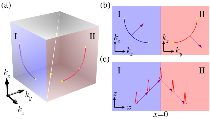
On both surfaces, the states are parallel to the -direction. Therefore, Fermi arcs states at a chemical potential within the bulk gap (henceforth taken at ) are also parallel to the -direction. Correspondingly, due to the chirality of the surface states, electrons are fully transmitted without backscattering at a junction between the surfaces I and II, see Fig. 1(b).
Next, we perform a rotational transformation to the effective bulk Hamiltonian Eq. (1). In this way, we retain the same open boundary conditions and describe generally-orientated Fermi arcs. A rotation about the axis by an angle is defined by with the rotation operator
| (7) |
As a result, the bulk Weyl points are located at and the states on surface I can be described by the effective Hamiltonian
| (8) |
where is the renormalized velocity and . The Fermi arc defined by is
| (9) |
and stretches between . Note that our approach of rotating the effective bulk model and calculating the resulting surface dispersion is verified using microscopic lattice model simulations, see Appendix B. Similarly, on surface II
| (10) |
and the Fermi arc is defined by
| (11) |
and stretches between . Note that the two Fermi arcs have different orientations; see Fig. 1. For a finite , electrons incident on surface I can only transfer through the interface due to the lack of backscattering channels. At the same time, because the Fermi arcs on the two surfaces tilt in opposite directions, the velocity in the -direction is inverted, leading to negative refraction as shown in Figs. 1(b) and (c).
In the following, we introduce a general dispersion term to the surface Hamiltonian
| (12) |
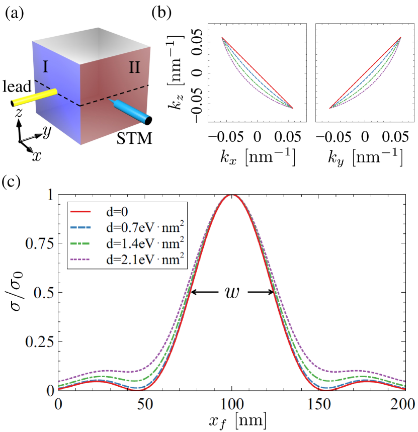
with a parabolic dispersion . By tuning the dispersion strength , the Fermi arcs become curved; see Figs. 1 and 2(b). Such curving captures the situation in real materials Lv et al. (2015a); Xu et al. (2015a, b, c, 2016); Deng et al. (2016); Yang et al. (2015); Huang et al. (2016); Tamai et al. (2016); Jiang et al. (2017); Belopolski et al. (2016); Lv et al. (2015b). Moreover, the velocities of the surface states are also modified. In our following calculation, we assume that the dispersion does not invert the velocity in the - (-) direction on surface I (II). Note that the description of generally orientated Fermi arcs by rotation of the effective model works for both - and -symmetric Weyl semimetals. This approach is verified by numerical simulations of corresponding lattice models (see Appendix B).
III Negative refraction in -symmetric Weyl semimetals
Next, we investigate nonlocal electron transport through the surface states, see the corresponding two-terminal setup in Fig. 2(a). For convenience, we unfold the two open surfaces to the plane with the boundary located at [Fig. 1(c)], which can be achieved by the replacement in Eq. (12). An electron wave packet is injected from the local lead at on surface I, then transmitted to surface II via negative refraction, and finally reaches the tip of the scanning tunneling microscope (STM) at . The wave packet propagates along a spatially-localized trajectory [cf. Fig. 1(c)]. This behavior can be revealed by the appearance of a peak structure in the spatially resolved non-local conductance as a function of [calculated below]; see Fig. 2(c). Crucially, this signature is unique to the negative refraction through the Fermi arc surface states. For normal metal states, the conductance decays with , as the wave packet expands in the -direction.
In the following, we calculate the non-local conductance using the surface Hamiltonian (12) and the Green’s function method. The Fermi energy is set to zero for simplicity, so that bulk electrons do not contribute to the conductivity. The finite density of the bulk states can solely lead to leakage of electrons, which will not change our main results. The coupling between the terminals and the surface states is described by a tunneling Hamiltonian as
| (13) |
where is the tunneling strength between the system and the terminal, is the Fermi operator in the terminal with momentum and is the field operator of the surface states at position , with corresponding to each terminal location.
The non-local conductance (including spin degeneracy) between local electrode and the STM tip is given by Datta (1997)
| (14) |
The full retarded () and advanced () Green’s function and the linewidth functions are [see Appendix C for details]
| (15) |
| (16) |
where the function with the density of states (DOS) of Fermi arc surface states per unit area and the DOS of the terminal at energy . The bare Green’s function are [cf. Eq. (49)]
| (17) |
with
| (18) |
Here, and are solved by and , respectively. The interval of integration covers the Fermi arc region, and the dependence of the velocity in the -direction is ignored.
Performing integration in Eq. (14) yields
| (19) | |||||
| (20) |
where takes the maximum value when . The dependence of on comes from the factor , which has a peak due to negative refraction; see Fig. 2(c). In particular, when , , one can see from Eq. (18) that the peak of the function is centered around on the axis. The peak structure in the non-local conductance stems from the wave packet trajectory of negative refraction in Fig. 1(c). The width of the peak , corresponding to the scale of the wave packet, is comparable with , which can be seen from Eq. (18). Specifically, in the case of straight Fermi arcs and , we will have . Performing the integration in Eq. (18) yields , thus the peak width for is comparable with . For curved Fermi arcs with dispersion (), the wave packet spreads during its propagation, so that the peak of conductance is broadened as well; see Fig. 2(c). Therefore, the peak width provides useful information about the length of the Fermi arcs. The existence of the peak structure is also confirmed numerically in Fig. 7(a).
IV Negative refraction in -symmetric Weyl semimetals
In reality, there are only few material candidates for Weyl semimetals with only two Weyl points Li et al. (2019); Wang et al. (2019); Soh et al. (2019). Hence, we investigate negative refraction between the surface states of -symmetric Weyl semimetals, which are more abundant Lv et al. (2015a); Xu et al. (2015a, c, 2016, b). Specifically, we study a semimetal with four Weyl points. Our results can be readily extended to the situation with more Weyl points.
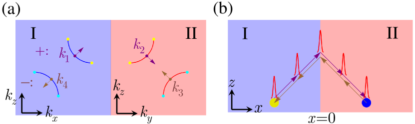
Consider a -symmetric Weyl semimetal with two pairs of Weyl points. Correspondingly, there are two Fermi arc segments on each open surface, which are the time-reversal counterpart to each other; see Fig. 3(a). The existence of two branches of surface states with opposite chirality enables backscattering between them. For simplicity, we restrict our discussion to the case that two Fermi arcs on the same surface do not overlap when projecting to the axis. It means that no backscattering occurs for conserved , so that perfect negative refraction occurs at the interface between surfaces I and II He et al. (2018). However, backscattering takes place at the local terminals, leading to Fabry-Pérot interference [Fig. 3(b)] and additional oscillation of the non-local conductance on top of the peak structure in real space.
More concretely, the two adjacent open surfaces I and II contains two Fermi arcs each, as shown in Fig. 3(a). We describe the branch “” by
| (23) |
which is similar to Eq. (12) except for a shift of the Fermi arcs in the surface Brillouin zone. The time-reversal counterpart, branch “” is described by .
Similar to the -symmetric case, we first solve the Green’s function for the surface states, yielding
| (24) |
with
| (25) |
where is the density of surface states per unit area, and and are the component of the terminations of the Fermi arcs in the branch “+”. and are solved by and , respectively. We describe the coupling to the terminals by the same tunneling Hamiltonian (13), which leads to the same self-energy in Eq. (C). The full Green’s function, however, takes a different form due to the backscattering at the terminals,
| (26) |
The resulting non-local conductance calculated by Eq. (14) is
| (27) |
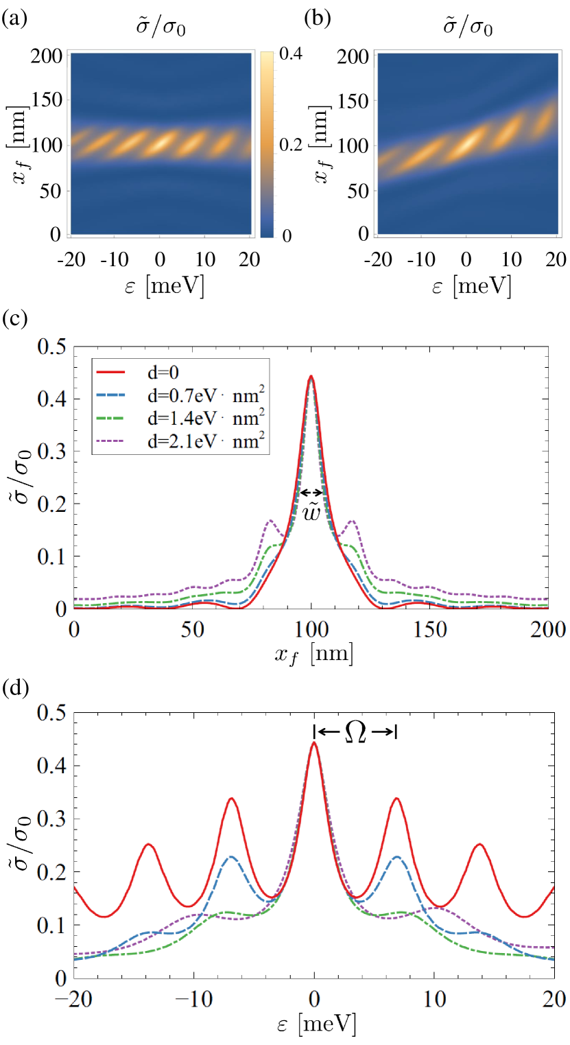
which mainly differs from the -symmetric Weyl semimetal [cf. Eq. (19)] by the additional term in the denominator due to the multiple scattering in Fig. 3(b). In the weak tunneling limit , the effect due to multiple scattering is negligible and the conductance More generally, the conductance as a function of energy and is plotted in Figs. 4(a) and 4(b). The non-local conductance displays additional Fabry-Pérot oscillations induced by multiple scattering on top of the peak structure in real space, resulting in the appearance of side peaks for large dispersion ; see Fig. 4(c), which is verified by numerical simulations using a lattice model in Fig. 7(b). The width of the main peak is comparable to for the same reason as in the -symmetric case. The Fabry-Pérot interference also results in oscillation of conductance with energy when is small [Figs. 4(a) and 4(d)], which is due to the dependence of the Fermi momenta on energy. Specifically, assume that, for the branch ”+”, the Fermi velocity along the x-direction [cf. Fig. 3], , is independent of . This implies that when the energy increases by the momenta and will increase by . Therefore, the function [cf. Eq. (25)] gains an additional phase factor of . Due to the factor in the denominator of Eq. (27), the oscillation period with , , is comparable with . Note that, in the case of large , the center of the resonant peak in real space moves with [Fig. 4(b)], and oscillation with cannot be seen due to the rapid decrease of the conductance at [Fig. 4(d)].
V Discussion and conclusion
So far, we have analyzed negative refraction based on the minimal model of - and -symmetric Weyl semimetals. Several important issues related to the experimental implementation of our proposal are discussed in the following:
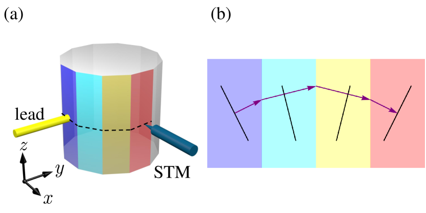
(i) Our scheme applies also to polyhedral nanowires with surfaces. When the Weyl nodes are aligned in a direction deviating from the central axis, the Fermi arcs on the surfaces become tilted and many refraction processes take place at the boundary of the facets, as shown in Fig. 5. While many of the refraction processes are normal refraction, one of them is negative refraction which leads to a spatially localized trajectory similar to Fig.1(c). The scheme should also hold at , when polyhedron becomes a cylinder.
(ii) For Weyl semimetals with more Weyl points and Fermi arcs than those obtained within the minimal model, as in most materialsLv et al. (2015a); Xu et al. (2015a, b, c, 2016); Deng et al. (2016); Yang et al. (2015); Huang et al. (2016); Tamai et al. (2016); Jiang et al. (2017); Belopolski et al. (2016); Lv et al. (2015b), our main results still hold as long as the overlap between the projections of different incident and reflection channels with conserved momentum is negligibly small. In this case, due to the different orientations of Fermi arcs and the corresponding trajectories of negative refraction, a multiple peak structure in the nonlocal conductance may appear in the same transport scheme in Fig. 2(a). The negative refraction will get suppressed if the overlap between the projections of the incident and reflection Fermi arcs is large due to the enhanced backscattering.
(iii) We considered Fermi arcs with a regular shape, such that electrons propagate on the surfaces towards certain directions, which is the main difference between Fermi arc states and normal metal states. For Weyl semimetals with long and winding Fermi arcs, surface transport will occur in different directions similar to normal metals, and negative refraction cannot be observed.
(iv) In real materials, the Fermi energy usually deviates from the Weyl points, resulting in a finite density of bulk states. Our result is not sensitive to such a deviation because the nonlocal transport occurs on the surface of the sample. The bulk states only lead to certain leakage of the injected electrons, and these leaked electrons do not follow the trajectory of negative refraction. As a result, their propagation does not have a peak structure in real space and they contribute only a small background to the conductance peak in the nonlocal transport. Such a small background will not change the qualitative results.
(v) By using Eqs.(2) and (3) as effective descriptions of the Fermi arc surface states we ignore the penetration of the surface states into the bulk. This is because in most intervals between the Weyl nodes the surface states are well-localized on the surface. Only in the vicinity of Weyl points, will the surface states possess a long penetration into the bulk. These states have no much difference from the bulk states and will not kill the signature of negative refraction as discussed in point (iv). Another effect of such penetration is that it effectively reduces the available transport channels on the surface or equivalently, the length of the Fermi arcs, which also does not change the main results.
(vi) Finally, surface imperfections such as dangling bonds may exist, which can be treated as disorder. In -symmetric Weyl semimetals, such surface disorder should have little effect on the negative refraction and the conductance peak remains stable. This is because the surface states are unidirectional and are thus immune to backscattering. However, in -symmetric Weyl semimetals surface disorder will lead to backscattering between the time-reversal counterpart of the Fermi arcs with opposite chirality, which reduces the negative refraction efficiency as well as the peak structure of the nonlocal conductance.
In summary, we have shown that perfect negative refraction, which can be realized on two adjacent surfaces of Weyl semimetals with properly oriented Fermi arcs, leads to distinct spatial trajectories for electron propagation. The space resolved peak structure of the nonlocal conductance which indicates the trajectory of negative refraction can serve as unique evidence of the Fermi arc states. Recent progress on Weyl semimetals with a single pair of Weyl nodes in MnBi2Te4Li et al. (2019) and EuCd2As2Wang et al. (2019); Soh et al. (2019) paves the way to the realization of our proposal. Furthermore, the manipulation of the negative refraction process offers potential applications of a Weyl semimetal nanowire as a field-effect transistorChen et al. (2020). Our work opens a new platform to study negative refraction in electronics Cheianov et al. (2007); Cserti et al. (2007); Beenakker (2008a); Lee et al. (2015). Compared with the existing physical systems, the negative refraction in Fermi arc states exhibit an unambiguous signature for its detection.
Acknowledgements.
We acknowledge financial support from the Swiss National Science Foundation through the Division II. We would like to thank Jose Lado for helpful discussions.Appendix A Derivation of Fermi arc states
We derive the Fermi arc surface state at an open surface in the direction Eq.(2) in the Weyl semimetal Eq.(1). The surface state at the open surface in the direction can be obtained similarly. To calculate the surface state we make the substitution to the Hamiltonian Eq.(1) since the existence of the open surface breaks translational symmetry in direction. Thus the surface state satisfies the following equation
| (28) |
with boundary conditions
| (29) |
Expanding on the basis
| (32) |
where and are the pseudo-spin components of , and substituting into Eq.(28), we have only for
| (35) |
Eq.(35) implies that
| (36) |
where , yielding two possible solutions of :
| (37) |
with . Among all possible linear combinations of with satisfying Eq.(37), the only one that satisfies the boundary conditions Eq.(29) is
| (40) |
with . To get the dispersion of the eigenstate 40, note that:
| (41) |
The self-consistent solution to Eqs.(37) and (41) is
| (42) |
with sgn being the sign function.
Appendix B Numerical calculation of Fermi arcs
In this Appendix, we verify numerically that for the - and - symmetric Weyl semimetals [cf. Eq. (1)], rotation of the effective bulk model leads to the oriented Fermi arcs on open surfaces.
For the -symmetric Weyl semimetal we adopt the the effective model in the article. For the -symmetric Weyl semimetal, we start with a minimal model
that has two Fermi arcs on each open surface. Then, we perform the following rotational transformation to the effective Hamiltonian to obtain generally-orientated Fermi arcs as with
| (47) |
The reason we apply instead of [cf. Eq. (7)] in the -symmetric case is because of different original positions of the Weyl points in the Brillouin zone to the -symmetric case.
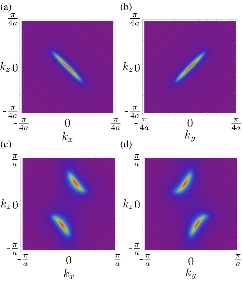
In the long-wavelength limit, the matching lattice model used in the numerical simulation can be constructed from the effective Hamiltonian through the substitution where is the lattice constant. The Fermi arcs of the -symmetric Weyl semimetal with (s.t. ) and -symmetric Weyl semimetal with are shown in Fig. 6.
Appendix C Green’s function calculation
For a fixed energy , the normalized eigenstate of the surface Hamiltonian is
| (48) |
where the momentum is conserved during the transmission, and and are solved by and , respectively. The function is the the Heaviside step function defining the two sides of the junction and is the combined area of surfaces I and II. Without coupling to the terminals, the bare Green’s functions can be constructed as
| (49) |
thus, describing electron propagation from to . Since the surface states are unidirectional, we have . By writing the sums as integrals we obtain Eq. (17) in the main text.
Appendix D Numerical simulations of non-local transport experiment
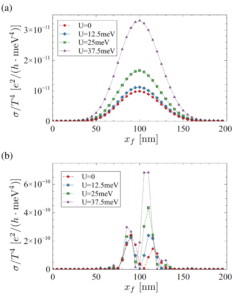
We compare our semiclassical analytical calculation approach with numerical simulations of the non-local transport experiment for both - and -symmetric Weyl semimetals and using the numerical package KWANT Groth et al. (2014). To be realistic, we adopt onsite potential to the first layer of the lattice on surface I (II) to introduce dispersion effects, which results in curved Fermi arcs. The non-local conductance under different choices of the onsite potentials is shown in Fig. 7. In both cases, the conductance peak value increases with the onsite potential, which is due to the increase of the surface DOS. In addition, in the symmetric case, the position of the peak varies for different onsite potential, which is due to the shift of the phase term in for dispersive Fermi arcs. In both cases, the peak structure persists for dispersive Fermi arcs, in agreement with the analytical results in Figs. 2 and 4.
Appendix E Introduction of surface dispersion from on-site potential
We show explicitly the on-site potentials we adopt on the surface of the Weyl semimetal in Appendix D result in the dispersion terms in Eq.(12). Note that the surface states on surface I possess a -dependent wave function that has some spatial profile along direction. Under surface potential , the potential that the states feel can be evaluated by the overlap integral , which is -dependent and thus serves as an effective dispersion . In our model, the surface states’ wavefunctions satisfy so that the effective dispersion is an even function of and , and takes the form to the second order in and . In addition, the dispersion term should vanish at Weyl points where the surface states spread in the whole bulk, which leads to . Therefore the surface potential leads to the dispersion in Eq.(12). Similarly, the surface potential leads to the dispersion in Eq.(12)
References
- Hasan and Kane (2010) M. Z. Hasan and C. L. Kane, Reviews of modern physics 82, 3045 (2010).
- Qi and Zhang (2011) X.-L. Qi and S.-C. Zhang, Reviews of Modern Physics 83, 1057 (2011).
- Armitage et al. (2018) N. P. Armitage, E. J. Mele, and A. Vishwanath, Rev. Mod. Phys. 90, 015001 (2018).
- Fang et al. (2016) C. Fang, H. Weng, X. Dai, and Z. Fang, Chinese Physics B 25, 117106 (2016).
- Wan et al. (2011) X. Wan, A. M. Turner, A. Vishwanath, and S. Y. Savrasov, Physical Review B 83, 205101 (2011).
- Murakami (2007) S. Murakami, New Journal of Physics 9, 356 (2007).
- Burkov and Balents (2011) A. A. Burkov and L. Balents, Phys. Rev. Lett. 107, 127205 (2011).
- Wang et al. (2013) Z. Wang, H. Weng, Q. Wu, X. Dai, and Z. Fang, Physical Review B 88, 125427 (2013).
- Weng et al. (2015) H. Weng, C. Fang, Z. Fang, B. A. Bernevig, and X. Dai, Phys. Rev. X 5, 011029 (2015).
- Huang et al. (2015) S.-M. Huang, S.-Y. Xu, I. Belopolski, C.-C. Lee, G. Chang, B. Wang, N. Alidoust, G. Bian, M. Neupane, C. Zhang, et al., Nature communications 6, 7373 (2015).
- Burkov et al. (2011) A. A. Burkov, M. D. Hook, and L. Balents, Phys. Rev. B 84, 235126 (2011).
- Lv et al. (2015a) B. Q. Lv, H. M. Weng, B. B. Fu, X. P. Wang, H. Miao, J. Ma, P. Richard, X. C. Huang, L. X. Zhao, G. F. Chen, Z. Fang, X. Dai, T. Qian, and H. Ding, Phys. Rev. X 5, 031013 (2015a).
- Xu et al. (2015a) S.-Y. Xu, I. Belopolski, N. Alidoust, M. Neupane, G. Bian, C. Zhang, R. Sankar, G. Chang, Z. Yuan, C.-C. Lee, et al., Science 349, 613 (2015a).
- Xu et al. (2015b) S.-Y. Xu, N. Alidoust, I. Belopolski, Z. Yuan, G. Bian, T.-R. Chang, H. Zheng, V. N. Strocov, D. S. Sanchez, G. Chang, et al., Nature Physics 11, 748 (2015b).
- Xu et al. (2015c) S.-Y. Xu, I. Belopolski, D. S. Sanchez, C. Zhang, G. Chang, C. Guo, G. Bian, Z. Yuan, H. Lu, T.-R. Chang, et al., Science advances 1, e1501092 (2015c).
- Xu et al. (2016) N. Xu, H. Weng, B. Lv, C. E. Matt, J. Park, F. Bisti, V. N. Strocov, D. Gawryluk, E. Pomjakushina, K. Conder, et al., Nature communications 7, 11006 (2016).
- Deng et al. (2016) K. Deng, G. Wan, P. Deng, K. Zhang, S. Ding, E. Wang, M. Yan, H. Huang, H. Zhang, Z. Xu, et al., Nature Physics 12, 1105 (2016).
- Yang et al. (2015) L. Yang, Z. Liu, Y. Sun, H. Peng, H. Yang, T. Zhang, B. Zhou, Y. Zhang, Y. Guo, M. Rahn, et al., Nature physics 11, 728 (2015).
- Huang et al. (2016) L. Huang, T. M. McCormick, M. Ochi, Z. Zhao, M.-T. Suzuki, R. Arita, Y. Wu, D. Mou, H. Cao, J. Yan, et al., Nature materials 15, 1155 (2016).
- Tamai et al. (2016) A. Tamai, Q. S. Wu, I. Cucchi, F. Y. Bruno, S. Riccò, T. K. Kim, M. Hoesch, C. Barreteau, E. Giannini, C. Besnard, A. A. Soluyanov, and F. Baumberger, Phys. Rev. X 6, 031021 (2016).
- Jiang et al. (2017) J. Jiang, Z. Liu, Y. Sun, H. Yang, C. Rajamathi, Y. Qi, L. Yang, C. Chen, H. Peng, C. Hwang, et al., Nature communications 8, 13973 (2017).
- Belopolski et al. (2016) I. Belopolski, D. S. Sanchez, Y. Ishida, X. Pan, P. Yu, S.-Y. Xu, G. Chang, T.-R. Chang, H. Zheng, N. Alidoust, et al., Nature communications 7, 13643 (2016).
- Lv et al. (2015b) B. Lv, N. Xu, H. Weng, J. Ma, P. Richard, X. Huang, L. Zhao, G. Chen, C. Matt, F. Bisti, et al., Nature Physics 11, 724 (2015b).
- Chen et al. (2018) W. Chen, K. Luo, L. Li, and O. Zilberberg, Physical review letters 121, 166802 (2018).
- Chen and Lado (2019) W. Chen and J. L. Lado, Phys. Rev. Lett. 122, 016803 (2019).
- Lu et al. (2013) L. Lu, L. Fu, J. D. Joannopoulos, and M. Soljačić, Nature photonics 7, 294 (2013).
- Lu et al. (2015) L. Lu, Z. Wang, D. Ye, L. Ran, L. Fu, J. D. Joannopoulos, and M. Soljačić, Science 349, 622 (2015).
- Xiao et al. (2015) M. Xiao, W.-J. Chen, W.-Y. He, and C. T. Chan, Nature Physics 11, 920 (2015).
- Yang and Zhang (2016) Z. Yang and B. Zhang, Physical review letters 117, 224301 (2016).
- Lee et al. (2018) C. H. Lee, S. Imhof, C. Berger, F. Bayer, J. Brehm, L. W. Molenkamp, T. Kiessling, and R. Thomale, Communications Physics 1, 39 (2018).
- Luo et al. (2018) K. Luo, R. Yu, H. Weng, et al., Research 2018, 6793752 (2018).
- Lu et al. (2019) Y. Lu, N. Jia, L. Su, C. Owens, G. Juzeliūnas, D. I. Schuster, and J. Simon, Phys. Rev. B 99, 020302 (2019).
- Balents (2011) L. Balents, Physics 4, 36 (2011).
- Yang et al. (2011) K.-Y. Yang, Y.-M. Lu, and Y. Ran, Phys. Rev. B 84, 075129 (2011).
- Moll et al. (2016) P. J. Moll, N. L. Nair, T. Helm, A. C. Potter, I. Kimchi, A. Vishwanath, and J. G. Analytis, Nature 535, 266 (2016).
- Wang et al. (2016) L.-X. Wang, C.-Z. Li, D.-P. Yu, and Z.-M. Liao, Nature communications 7, 10769 (2016).
- Bovenzi et al. (2017) N. Bovenzi, M. Breitkreiz, P. Baireuther, T. E. O’Brien, J. Tworzydło, i. d. I. Adagideli, and C. W. J. Beenakker, Phys. Rev. B 96, 035437 (2017).
- Faraei and Jafari (2019) Z. Faraei and S. A. Jafari, Phys. Rev. B 100, 035447 (2019).
- Adinehvand et al. (2019) F. Adinehvand, Z. Faraei, T. Farajollahpour, and S. A. Jafari, Phys. Rev. B 100, 195408 (2019).
- Chen et al. (2020) G. Chen, W. Chen, and O. Zilberberg, APL Materials 8, 011102 (2020), https://doi.org/10.1063/1.5126033 .
- He et al. (2018) H. He, C. Qiu, L. Ye, X. Cai, X. Fan, M. Ke, F. Zhang, and Z. Liu, Nature 560, 61 (2018).
- Li et al. (2019) J. Li, Y. Li, S. Du, Z. Wang, B.-L. Gu, S.-C. Zhang, K. He, W. Duan, and Y. Xu, Science Advances 5, eaaw5685 (2019).
- Wang et al. (2019) L.-L. Wang, N. H. Jo, B. Kuthanazhi, Y. Wu, R. J. McQueeney, A. Kaminski, and P. C. Canfield, arXiv preprint arXiv:1901.08234 (2019).
- Soh et al. (2019) J.-R. Soh, F. de Juan, M. Vergniory, N. Schröter, M. Rahn, D. Yan, M. Bristow, P. Reiss, J. Blandy, Y. Guo, et al., arXiv preprint arXiv:1901.10022 (2019).
- Morali et al. (2019) N. Morali, R. Batabyal, P. K. Nag, E. Liu, Q. Xu, Y. Sun, B. Yan, C. Felser, N. Avraham, and H. Beidenkopf, arXiv preprint arXiv:1903.00509 (2019).
- Yang et al. (2019) H. Yang, L. Yang, Z. Liu, Y. Sun, C. Chen, H. Peng, M. Schmidt, D. Prabhakaran, B. Bernevig, C. Felser, et al., Nature communications 10, 1 (2019).
- Cheianov et al. (2007) V. V. Cheianov, V. Fal’ko, and B. Altshuler, Science 315, 1252 (2007).
- Cserti et al. (2007) J. Cserti, A. Pályi, and C. Péterfalvi, Physical review letters 99, 246801 (2007).
- Beenakker (2008a) C. W. J. Beenakker, Rev. Mod. Phys. 80, 1337 (2008a).
- Lee et al. (2015) G.-H. Lee, G.-H. Park, and H.-J. Lee, Nature Physics 11, 925 (2015).
- Chen et al. (2013) W. Chen, L. Jiang, R. Shen, L. Sheng, B. Wang, and D. Xing, EPL (Europhysics Letters) 103, 27006 (2013).
- Datta (1997) S. Datta, Electronic transport in mesoscopic systems (Cambridge university press, 1997).
- Groth et al. (2014) C. W. Groth, M. Wimmer, A. R. Akhmerov, and X. Waintal, New Journal of Physics 16, 063065 (2014).