From Andreev to Majorana bound states in hybrid superconductor-semiconductor nanowires
Abstract
Electronic excitations above the ground state must overcome an energy gap in superconductors with spatially-homogeneous -wave pairing. In contrast, inhomogeneous superconductors such as those with magnetic impurities or weak links, or heterojunctions containing normal metals or quantum dots, can host subgap electronic excitations that are generically known as Andreev bound states (ABSs). With the advent of topological superconductivity, a new kind of ABS with exotic qualities, known as Majorana bound state (MBS), has been discovered. We review the main properties of ABSs and MBSs, and the state-of-the-art techniques for their detection. We focus on hybrid superconductor-semiconductor nanowires, possibly coupled to quantum dots, as one of the most flexible and promising experimental platforms. We discuss how the combined effect of spin-orbit coupling and Zeeman field in these wires triggers the transition from ABSs into MBSs. We show theoretical progress beyond minimal models in understanding experiments, including the possibility of different types of robust zero modes that may emerge without a band-topological transition. We examine the role of spatial non-locality, a special property of MBS wavefunctions that, together with non-Abelian braiding, is the key to realizing topological quantum computation.
I Introduction
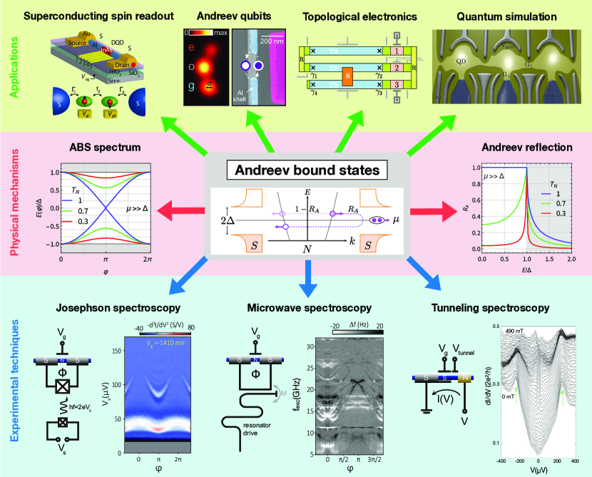
Ever since Kamerlingh Onnes discovered the “zero resistance state” of metals at very low temperatures in 1911 Kamerlingh Onnes (1911); van Delft and Kes (2010), the superconducting state of matter De Gennes (2018); Tinkham (2004) has fascinated physicists. In the last century, the understanding of superconductivity has evolved extraordinarily and has garnered eight Nobel prizes, turning it into one of the most iconic topics in condensed matter physics Martin (2019). As described by the seminal Bardeen-Cooper-Schrieffer (BCS) theory of superconductivity Bardeen et al. (1957), the characteristic feature of superconductors (SCs) is the macroscopic occupation of bound pairs of electrons, known as Cooper pairs Cooper (1956), in the same quantum-coherent ground state. The condensation of Cooper pairs into such ground state is associated with a superconducting complex order parameter Ginzburg and Landau (1950); Cyrot (1973), where is the conjugate of the number of Cooper pairs. In a homogeneous -wave BCS SC, the spectrum of single-particle excitations above the ground state develops an energy gap . These gapped excitations are propagating superpositions of electrons and holes with different energy-dependent weights. However, if the order parameter –also called the pair potential De Gennes (2018)– varies in space, , lower energy (‘subgap’) excitations may develop. Such is the case of states trapped in magnetic flux vortices (so-called Caroli-Matricon-De Gennes states Caroli et al. (1964)), at magnetic domains or impurities (Yu-Shiba-Rusinov states Yu (1965); Shiba (1968); Rusinov (1969)), at weak links between SCs or at normal metal-superconductor (NS) contacts Blonder et al. (1982), to name a few. Collectively, these subgap states are dubbed Andreev bound states (ABSs), and are the focus of numerous theoretical and experimental works, as well as the basis of promising emerging quantum technologies, see Fig. 1.
The core physical mechanism behind the formation of ABSs in inhomogeneous systems with is a remarkable scattering process, predicted by Andreev Andreev (1964, 1966), in which an incoming particle-like excitation can convert into an outgoing hole-like one and viceversa, see central row of Fig. 1. Many of such Andreev scattering events coherently concatenated lead to the formation of subgap ABSs De Gennes and Saint-James (1963); Kulik (1970) that are localized near the region where the pair potential has strong spatial variations (for a recent review see Sauls (2018)).
In the last decade, a new twist in the possibilities afforded by the superconducting pairing of electrons has been possible with the advent of topological materials Hasan and Kane (2010); Qi and Zhang (2011). Inspired by notions of topology Thouless et al. (1982), several authors have predicted the existence of new states of matter known collectively as topological superconducting phases, see Refs. Leijnse and Flensberg (2012); Alicea (2012); Beenakker (2013); Sato and Fujimoto (2016); Aguado (2017); Sato and Ando (2017) for reviews. These arise in particular in so-called -wave SCs, which possess a rare triplet-like pair potential (an exotic form of superconductivity involving only a single spin band Salomaa and Volovik (1988); Volovik and Volovik (2009); Read and Green (2000); Kitaev (2001); Sato and Fujimoto (2009)). Topological SC phases are characterized by the emergence of a rather special type of subgap bound state occurring at topological defects such as vortices, boundaries or domain walls. Importantly, such bound states occur precisely at zero energy, and exhibit electron and hole character with exactly equal probability. The second quantization operators describing these states are self-conjugate, . They are in this sense a condensed matter realisation of the celebrated ‘particle-equals-antiparticle’ states known as Majorana fermions Majorana (1937), and also of so-called Jackiw-Rossi states at field vortices in the Dirac equation Nishida et al. (2010); Jackiw and Rossi (1981).
As opposed to standard ABSs, which can be pushed out of the gap by continuous deformations of the Hamiltonian, Majorana bound states (MBSs) cannot be removed from zero energy by any local perturbation or local noise that does not close the gap. This robust zero-energy pinning is a consequence of the bulk-boundary correspondence principle of band topology Fukui et al. (2012), which predicts that at the boundaries between materials with different topological indices, edge states must appear that are protected against perturbations by the topology of the bulk. Quite remarkably, MBSs do not follow fermion statistics, unlike the original particles predicted by Majorana Majorana (1937), but rather possess non-Abelian exchange statistics. Upon exchange of two MBSs (braiding), a non-trivial unitary operation will be performed on them. This property, together with their topological protection against local noise, holds promise for applications in fault-tolerant quantum computing Kitaev (2003); Nayak et al. (2008).
The interesting connection between Dirac physics, superconductivity and Majorana zero modes was exploited by Fu and Kane in 2008 Fu and Kane (2008), who put forward the conceptual breakthrough of effectively creating -wave superconductivity and MBSs out of standard -wave SCs by virtue of the proximity effect acting onto the helical edge states of topological insulators (propagating edge states with spin-momentum locking). The possibility of combining different materials to engineer the topological superconducting state has spurred immense interest in the physics of Majorana states in hybrid systems.
Fu and Kane’s idea was soon extended to other materials with helical states produced by strong spin-orbit (SO) coupling, but different from topological insulators Sato and Fujimoto (2009). A popular practical proposal was put forward independently by two groups in 2010 (Lutchyn et al. Lutchyn et al. (2010) and Oreg et al. Oreg et al. (2010)), that realizes the conceptual model for one-dimensional (1D) -wave superconductivity proposed by Kitaev in 2001 Kitaev (2001). It was based on 1D low-density semiconducting nanowires under an external magnetic field , which readily allowed its implementation in experiments. The combination of the SO interaction and the Zeeman field associated to generates, for a small chemical potential in the nanowire, a helical phase similar to that of topological insulators but with broken time-reversal symmetry Středa and Šeba (2003). By covering the nanowire with a conventional SC, its spectrum becomes gapped by the proximity effect. In this device, sometimes dubbed a Majorana nanowire, a topological transition in the form of a band inversion was predicted to occur at a critical Zeeman energy of the order of the induced superconducting gap (Box A). The material properties necessary to realize this proposal in the lab can be achieved by using e.g. InAs or InSb semiconducting nanowires Stanescu and Tewari (2013a); Lutchyn et al. (2018). Hybrid superconducting-semiconducting devices based on such nanowires can be tuned to the topological phase by increasing and depleting the wires by means of gate voltages. In finite, but sufficiently long wires, zero energy MBSs emerge in pairs for , one localized at either end. One pair of Majorana states forms a non-local fermion. The occupation of two such fermions defines the elementary qubit in proposals of topological quantum computers Kitaev (2001).
In this work we review the formation and properties of general subgap bound states in nanowires and nanowire junctions, as they evolve from conventional ABSs in high-density nanowires (Sec. II) to topological Majorana zero modes at low-densities and finite magnetic fields (Sec. III). We summarize the main experimental approaches currently used for their detection and characterization Mourik et al. (2012); van Woerkom et al. (2017); Tosi et al. (2019), including ABSs in nanowire quantum dots (QDs) Lee et al. (2012, 2014, 2017a); Grove-Rasmussen et al. (2018); Su et al. (2018); Jünger et al. (2019). Going beyond, we discuss in Sec. IV various physical extensions of the minimal description of Majorana nanowires. These include multimode effects Potter and Lee (2010, 2011); Lutchyn et al. (2011); Lutchyn and Fisher (2011), renormalized -factors and SO couplings due to strong proximity effect with the parent SC Cole et al. (2015); Reeg et al. (2017, 2018a); Vaitiekenas et al. (2018); Antipov et al. (2018); Dmytruk et al. (2018); Pan et al. (2019), effects of the charge density distribution across the wire section and of the electrostatic environment Vuik et al. (2016); Domínguez et al. (2017a); Mikkelsen et al. (2018); Antipov et al. (2018); de Moor et al. (2018); Woods et al. (2018); Escribano et al. (2018); Winkler et al. (2019) or density and pairing inhomogeneities Prada et al. (2012); Kells et al. (2012); Stanescu and Tewari (2013b); Roy et al. (2013); Fleckenstein et al. (2018). Such generalized nanowires have been predicted to sometimes develop robust zero modes Prada et al. (2012); Kells et al. (2012); Stanescu and Tewari (2013b); Roy et al. (2013); Stanescu and Tewari (2014); Liu et al. (2017a); Fleckenstein et al. (2018); Peñaranda et al. (2018); Reeg et al. (2018b); Liu et al. (2018); Moore et al. (2018a, b); Vuik et al. (2019); Awoga et al. (2019); Avila et al. (2019); Stanescu and Tewari (2019); Woods et al. (2019) that cannot be classified using the band-topological concepts of uniform Majorana nanowires. They allow nevertheless a classification within the more general context of non-Hermitian topology Avila et al. (2019). We review the open questions that remain as to their nature (e.g. their location within the wire Stanescu and Tewari (2013b); Peñaranda et al. (2018); Fleckenstein et al. (2018); Moore et al. (2018a); Reeg et al. (2018b); Vuik et al. (2019); Stanescu and Tewari (2019); Woods et al. (2019), their degree of fermionic non-locality Prada et al. (2017); Peñaranda et al. (2018); Deng et al. (2018), their decay into external leads San-Jose et al. (2016); Avila et al. (2019), their resilience to perturbations Goldstein and Chamon (2011); Budich et al. (2012); Rainis and Loss (2012); Trif and Tserkovnyak (2012); Schmidt et al. (2012, 2013); Scheurer and Shnirman (2013); Pedrocchi and DiVincenzo (2015); Dmytruk et al. (2015); Sekania et al. (2017); Knapp et al. (2018); Aseev et al. (2018); Lai et al. (2018); Aseev et al. (2019)) and the conditions for their emergence. Understanding these zero modes without a clear relation to bulk topology is particularly important currently, in view of the many observations of robust zero bias anomalies reported in recent experiments Deng et al. (2016); Nichele et al. (2017); Zhang et al. (2017).
Although we focus on semiconductor nanowires in this review, we note that MBSs are also investigated in other material platforms, including atomic chains Nadj-Perge et al. (2013, 2014), monolayer islands Ménard et al. (2017, 2019); Palacio-Morales et al. (2019), topological insulators Fu and Kane (2009); Wiedenmann et al. (2016) and planar semiconductor heterostructures Suominen et al. (2017); Nichele et al. (2017), while ABSs were studied in e.g. atomic point contacts Bretheau et al. (2013); Janvier et al. (2015), carbon nanotubes Pillet et al. (2010); Eichler et al. (2007), graphene Dirks et al. (2011), and nanoparticles Deacon et al. (2010).
II ABSs in high-density nanowires and QDs
II.1 Formation of ABSs
ABSs arise in superconducting systems as the result of an unusual form of quantum confinement caused by so-called Andreev reflection Andreev (1964, 1966). In a metallic system in its normal phase, electrons become specularly reflected at planar interfaces with vacuum or insulating materials. This is known as normal reflection. However, at an NS boundary Kümmel (1969); Blonder et al. (1982), an incoming electron from the N side may transform into an outgoing hole with inverted spin and wave vector. This hole is said to be retro-reflected since both the parallel and normal velocity components to the interface change sign, whereas in a normal reflection the parallel component remains the same. This process is known as Andreev reflection, and is accompanied by the injection of a Cooper pair into the SC. If the interface is highly transparent, below the gap such Andreev process dominates with high probability , whereas in the opposite limit the electron becomes normal-reflected (), see central panel of Fig. 1. Experimentally, can be characterized based on the finite subgap conductance of the NS interface Zhang et al. (2017). The bias-dependent conductance of short nanowire segments between two SC leads was also used to extract the magnitude of , close to one, in various semiconductor nanowires, including SiGe Xiang et al. (2006); Ridderbos et al. (2019), InAs Jespersen et al. (2009); Doh et al. (2005); Günel et al. (2012); Goffman et al. (2017) and InSb Nilsson et al. (2012); Deng et al. (2012).
Consider now an electron in a normal metal between two or more insulating interfaces. When the metallic region is small, multiple coherent normal reflections on the boundaries leads to the formation of electronic states of quantized energy. A similar process takes place when some or all of the confining insulators are replaced by SC boundaries Andreev (1966). This leads to the formation of ABSs, which are the superconducting analogue of the above particle-in-a-box states of quantum mechanics.
The formation of ABSs becomes particularly simple in the common case of high density SCs with negligible SO coupling and zero magnetic field. In such systems the superconducting gap is much smaller than the chemical potential, , a condition known as the Andreev limit Beenakker (1992a). The NS Andreev reflection probability then exhibits a simple dependence with normal-state junction transparency and energy (relative to the SC chemical potential), see Fig. 1 central-right panel. It reaches at from at Beenakker (1992b). This result assumes a step-like pair potential at the interface, a common approximation known as the rigid boundary-condition Likharev (1979).
We now combine two such NS interfaces into a 1D SNS junction with normal length . A computation in the Andreev limit of the energy of ABSs below for fully transparent interfaces, and as a function of SC phase difference across the junction, yields the following quantization condition Kulik (1970)
| (1) |
where is an integer and is the superconducting coherence length. A generalization to a multimode junction of finite transparency yields, in the short junction limit Kulik (1970); Furusaki and Tsukada (1991); Beenakker and van Houten (1991); Beenakker (1992a); Bagwell (1992); Furusaki (1999), an explicit solution for mode
| (2) |
where is the normal transmission for each independent scattering-matrix eigenmode in the normal phase Landauer (1981). The presence of such bound states has important consequences for transport, since, as argued by Kulik Kulik (1970), it implies that a normal metal can carry a dissipationless supercurrent between two SCs over arbitrarily long lengths, provided that transport is coherent. This is the celebrated dc Josephson effect Josephson (1962, 1965). At zero temperature and neglecting the contribution to the supercurrent coming from the continuum of states above , (where the factor 2 accounts for spin degeneracy).
Figure 1 central-left panel illustrates the solution for different in a single-channel junction. Near the ABSs touch the continuum of single quasiparticle states above while they reach their minimum value at , with an that decreases with increasing transparency until reaching an accidental zero-energy crossing as (assuming ). It is important to realize that, since , the ABS wavefunctions are confined to the junction, and exponentially decay into the bulk of the SC leads on a length scale .
Deviations from the Andreev limit, relevant in low-density nanowires, introduce important corrections to the Andreev reflection and ABS energies , and will be discussed in Sec. III.
II.2 ABS spectroscopy
Several measurement techniques have been developed to obtain information about ABSs in nanowire Josephson junctions. Here we focus on three broad classes: Josephson spectroscopy, microwave spectroscopy and tunneling spectroscopy, see bottom row of Fig. 1.
In a Josephson junction, parity-conserving transitions between the ground and excited states with an addition energy of [see Eq. (2)] can be created by an incident photon with a frequency of , where is Planck’s constant. Note that the SC gap eV of Al corresponds to a frequency range of GHz. A precise treatment of the pair transition leads to an effective microwave impedance associated with the transition Kos et al. (2013). It can be detected via the inelastic Cooper-pair tunneling Hofheinz et al. (2011) in a capacitively coupled auxiliary Josephson junction Holst et al. (1994), which is sensitive to the environmental impedance seen by this spectrometer junction. The probing frequency can be set by applying a voltage bias of (Fig. 1 lower-left panel). Measurements of this type confirmed the applicability of the short junction formula Eq. (2) in a wide range of excitation energies in InAs semiconductor channels with epitaxial Al leads and demonstrated that few-channel configurations of high channel transparency can be attained van Woerkom et al. (2017).
The Andreev two-level system [Eq. (2)] can also be characterized and manipulated by the well-established toolbox of circuit quantum electrodynamics Blais et al. (2004), based on the coupling between a resonator with frequency and the junction hosting the Andreev level. In the lowest order, this coupling is described by the Hamiltonian , where is the mutual inductance (Fig. 1 lower-central panel), and , are the current operators of the Andreev level (see Sec. II.1) and the resonator, respectively. It is instructive to note that the supercurrent changes sign between the ground and excited state. Furthermore, the odd parity state with an unpaired quasiparticle yields . These three states can then be distinguished by the dispersive frequency shift of the coupled resonator, enabling a real time tracking of the junction charge parity Hays et al. (2018). The characteristic parity lifetimes are measured to be in excess of s in InAs nanowire Josephson junctions. In the same experiment, typical relaxation times ranging up to s allowed for the coherent manipulation of the nanowire-based Andreev level quantum bit.
Direct quasiparticle tunneling into the ABSs can also probe the ABS spectrum (Fig. 1 lower-right panel). These experiments utilize a gate-defined depleted section of the nanowire Mourik et al. (2012) or an in-situ grown axial tunnel barrier Car et al. (2017); Jünger et al. (2019) as the opaque probe junction. This measurement geometry allows for the characterization of energy spectra in proximitized semiconductor segments Chang et al. (2015) or quantum dots Lee et al. (2014); Grove-Rasmussen et al. (2018), and makes non-local correlation experiments possible Anselmetti et al. (2019). However mesoscopic interference effects in the leads may yield additional features in the differential conductance Su et al. (2018).
It is worth noting that the ABS spectrum can indirectly be characterized via the measurement of the phase-dependent supercurrent , which was performed by an inductively coupled SQUID loop Spanton et al. (2017); Hart et al. (2019). These experiments yielded strongly skewed current-phase relations, the signature of highly transparent channels in an InAs nanowire with Al superconducting leads. Similarly, the Josephson inductance, could serve as another probe of the anharmonicity in the current phase relationship Rifkin and Deaver (1976). Finally, external tunnel barriers, typically AlOx of a few atomic layers, attached to a metallic probe also became an established technique to detect ABSs in other systems, such as carbon nanotubes Pillet et al. (2010) and graphene flakes Dirks et al. (2011).
II.3 ABSs in QDs
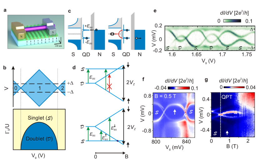
For the junctions above, it was assumed that the channel connecting the SC leads allowed for coherent transport through a ballistic nanowire segment. By contrast, in QDs, charges localize in the channel and the effect of a finite electrostatic charging energy must be taken into account. QDs can be formed in a nanowire by e.g. inducing barriers with electrostatic gates [Fig. 2(a)]. At low temperatures and for low bias voltages, transport is blocked by the large and the system is in the so-called Coulomb blockade regime with a well defined number of electrons . Current flow is only possible at discrete degeneracy points where the energies of the and charge states become degenerate. Given the strong confinement in nanoscale QDs, can easily exceed in the electrodes, resulting in an interesting interplay between single-electron charge transport, localized spins and superconductivity De Franceschi et al. (2010).
The formation of ABSs can be understood by considering a single QD level coupled to a superconducting electrode. If the level is singly occupied, it holds an unpaired spin, i.e. a spin-doublet ground state [Fig. 2 (b)]. Conceptually, this scenario is identical to having an isolated magnetic impurity in a superconducting host. As shown by Yu, Shiba and Rusinov (YSR) in the 1960s Yu (1965); Shiba (1968); Rusinov (1969), the magnetic impurity induces localized bound states within the SC gap. At a critical exchange coupling the system undergoes a quantum phase transition to a magnetically screened, spin-singlet ground state. Conversely, at weaker coupling, the system maintains its original doublet state. While the above YSR picture applies for classical magnetic impurities, a full quantum treatment naturally leads to the physics of the Kondo effect Hewson (1993) where, despite the absence of screening electrons within of the electrodes, the localized spin can still be screened by the above-gap quasiparticles in the SC. As in normal metals, Kondo physics sets in below a characteristic temperature , which results in singlet-doublet transitions occurring at . Early work on hybrid dots indicated the importance of Kondo-like correlations Buitelaar et al. (2002); Sand-Jespersen et al. (2007), while more recent experimental work has provided precise boundaries for the transition Lee et al. (2017a). Figure 2(b) shows the generic phase diagram of a hybrid QD as a function of dot parameters Zitko et al. (2015); Lee et al. (2014, 2017a).
ABSs in QDs can be detected by transport spectroscopy Eichler et al. (2007); Grove-Rasmussen et al. (2009); Pillet et al. (2010); Deacon et al. (2010); Chang et al. (2013); Lee et al. (2014); Kumar et al. (2014); Jellinggaard et al. (2016); Li et al. (2017); Island et al. (2017), whereby is measured as a function of bias voltage . The sub-gap transport reflects resonant Andreev reflection processes at voltages matching the energy difference between the ground and the excited state of the QD [Figs. 2 (c) and (d)]. This results in peaks located symmetrically around , corresponding to ABS resonances at energies . Figure 2 (e) shows a typical transport spectrum, where ABSs are visible as ridges below the gap. As the charge state, and thereby the parity, of the dot is tuned, the ground state switches between the singlet and doublet states, as reflected by the ABS crossings at zero bias. Remarkably, the ground state remains a singlet in some odd-occupancy regions due to the strong screening discussed above, which leads to avoided ABS crossings in the spectra. The experimental phase diagram of the QD-S system has been explored Lee et al. (2017a); Jellinggaard et al. (2016); Li et al. (2017), finding excellent quantitative agreement with theory Andersen et al. (2011); Zitko et al. (2015). In some cases, however, one needs to go beyond the bulk treatment of the SC above (to include soft gaps, finite-length effects, etc) in order to understand the complex ABS spectra of finite-length proximitized nanowires Su et al. (2018); Jünger et al. (2019). Transport spectroscopy of ABSs can also be performed by replacing the N probe by a weakly coupled superconductor. Here, all spectroscopical features are shifted by Lee et al. (2012); Kumar et al. (2014). ABSs exist also in coupled hybrid dot systems Su et al. (2017); Grove-Rasmussen et al. (2018) where one can observe YSR screening of higher spin states and a more intricate phase diagram than Fig. 2 (b) Grove-Rasmussen et al. (2018); Saldaña et al. (2018). We note that YSR states have also been studied in STM experiments as reviewed e.g. in Ref. Heinrich et al. (2018).
In an external magnetic field, the Zeeman effect lifts the spin degeneracy of the doublet state. This strongly impacts the transport spectra of the ABSs [Fig. 2(d)]. In case of a singlet ground state, two (parity-changing) transitions are allowed, thanks to the splitting of the excited doublet state. In contrast, when the ground state is a doublet, only one transition remains accessible independent of . As a result, the ABSs shift to higher energies but do not split. Figure 2 (f) depicts these two distinct behaviors of the ABSs at finite Lee et al. (2014). Interestingly, for high enough fields, the lowest-energy, spin-split ABSs can cross the Fermi level, denoting a quantum phase transition from the singlet ground state to a spin-polarized state Lee et al. (2014); Jellinggaard et al. (2016). This transition represents a parity crossing and appears as a zero-bias peak at the critical field [Fig. 2 (g)]. While the transition is a true crossing, the peak can persist at for a wider range of owing to the broadening of ABS resonances or to repulsion with other states or the gap edge Lee et al. (2014); Jellinggaard et al. (2016); Chen et al. (2019).
In addition to the above ABS spectroscopy, the physics of a hybrid QD can also be captured by measurements of the Josephson supercurrent in a S-QD-S geometry van Dam et al. (2006); Delagrange et al. (2015); Maurand et al. (2012); Estrada Saldaña et al. (2019). Notably, QDs have also been used to investigate MBSs in various device configurations Deng et al. (2012, 2014, 2016, 2018).
III Low-density nanowires and MBSs
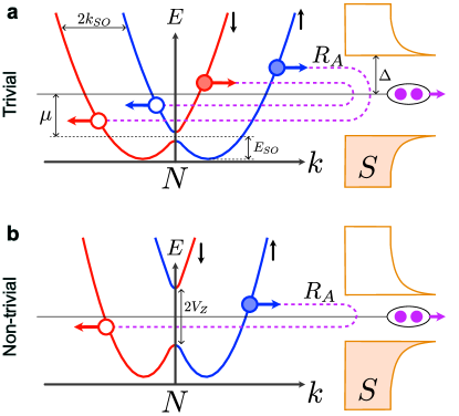
III.1 ABSs in trivial SNS junctions with SO coupling and Zeeman field
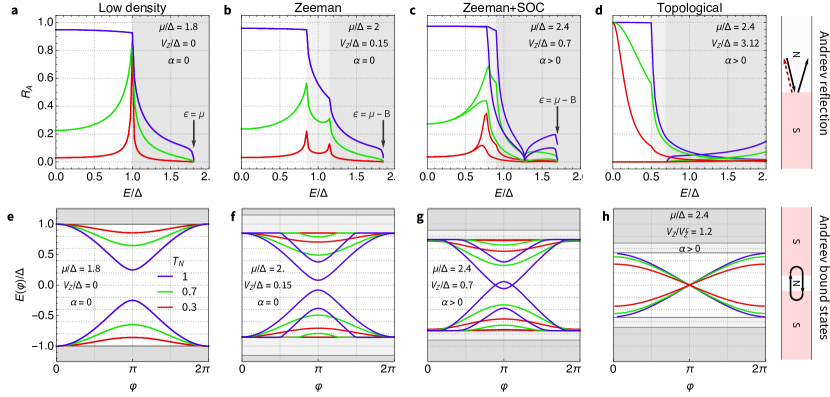
As the Fermi energy of a nanowire SNS junction is reduced (low density regime), it may become comparable to other energy scales in the problem, such as the SO energy (where is the SO coupling and the effective mass), the Zeeman energy at the junction, or the gap of the SCs at either side, see Box Fig. 7. The Andreev reflection at a low-density NS interface deviates considerably from the standard picture described in Sec. II.1. Figure 3 (a-c) shows the typical dependence of with energy for a single channel contact when both N and SC sides have a common Fermi energy, SO coupling and Zeeman. Similarly, the Andreev spectrum of the corresponding low-density SNS nanowire junction is no longer well described by the conventional Eq. (2), even in the short junction limit, see Fig. 3 (e-g). Note in particular that the parity crossing present at in high-density transparent junctions becomes an anticrossing even at as soon as the Andreev limit is not satisfied. This contrasts with the protected (-independent) crossing in topological SNS junctions, as we will see.
To understand the main low-density corrections we consider first the case of an SNS junction in which becomes comparable to the SO energy , while still remaining in the Andreev limit . We further consider the realistic complication that the SO coupling and the Zeeman field are largely confined to the normal part of the nanowire. The Fermi energy in N is also assumed to differ from that of the SC contacts . The corresponding bandstructures will thus exhibit a Fermi momentum mismatch, which reduces Andreev reflection and affects the resulting ABS spectrum. In a nominally perfect, single mode SNS junction of nanowire length with , Eq. (2) can be generalized to Cheng and Lutchyn (2012)
| (3) |
where captures the effect of momentum mismatch acting as an effective barrier at each interface, with a transmission that is smaller than , except at resonant values of the nanowire length , . Here the SC and N Fermi wavevectors are , and . This depends also on the SO momentum , that captures the momentum band shift of the two spin sectors in the nanowire (see Box A). of Eq. (3) remains doubly degenerate for all despite the shift of the two spin sectors; electron-hole pairs can still form in a similar manner as for a spin-degenerate single parabolic dispersion, see Fig. 7. While Eq. (3) still yields a zero energy crossing at and , it captures the fact that even with nominally perfect contacts due to the momentum mismatch.
In the absence of a Zeeman field, spin splitting of the ABS spectrum can be achieved by a nonzero in a two-subband model with intersubband coupling. Specifically, mixing between the two lowest transverse subbands in a low density regime may produce a strongly spin-dependent Fermi velocity , and hence coherence lengths , which leads to spin-dependent quantization conditions according to Eq. (1). For , and assuming or , the ABSs can be written as Park and Levy Yeyati (2017)
| (4) |
The spin splitting between ABSs reads
| (5) |
This phase-dependent spin splitting is finite for , and comes from the difference in coherence lengths and Fermi velocities. Spin-degeneracy at and is protected by time-reversal symmetry. The combined effect of Zeeman and SO coupling on the Andreev level spectra of single channel nanowires has been studied in Ref. van Heck et al. (2017); Dmytruk et al. (2018). Among others, an important consequence of the interplay of and is the strong suppression of the -factor owing to SO coupling and/or high electron density. This -factor renormalization drastically changes the spin splitting of Andreev levels for increasing magnetic fields.
III.2 Emergence of MBSs
In Fig. 3 (e-g) we have illustrated the strong effect of SO coupling and Zeeman fields in the ABS spectrum of a low-density SNS nanowire junction. When the SC contacts are taken as low-density proximitized nanowires, the Oreg-Lutchyn minimal model predicts that a sufficiently strong will make them undergo a topological phase transition, with MBSs at each interface. Their presence results in a topologically protected Andreev reflection amplitude at , see Fig. 3 (d), and a protected parity crossing of SNS ABSs for all transparencies, (h). The parity crossing is robust regardless of the microscopic channel configuration of the junction, and ideally gives rise to the topological Josephson effect, characterized by -periodic supercurrents as a function of at fixed parity Kitaev (2001); Kwon et al. (2004); Lutchyn et al. (2010); Oreg et al. (2010). The -periodic solution in the trivial phase, Eq. (2), transforms in the topological regime into , with different signs for opposite parities Kwon et al. (2004).
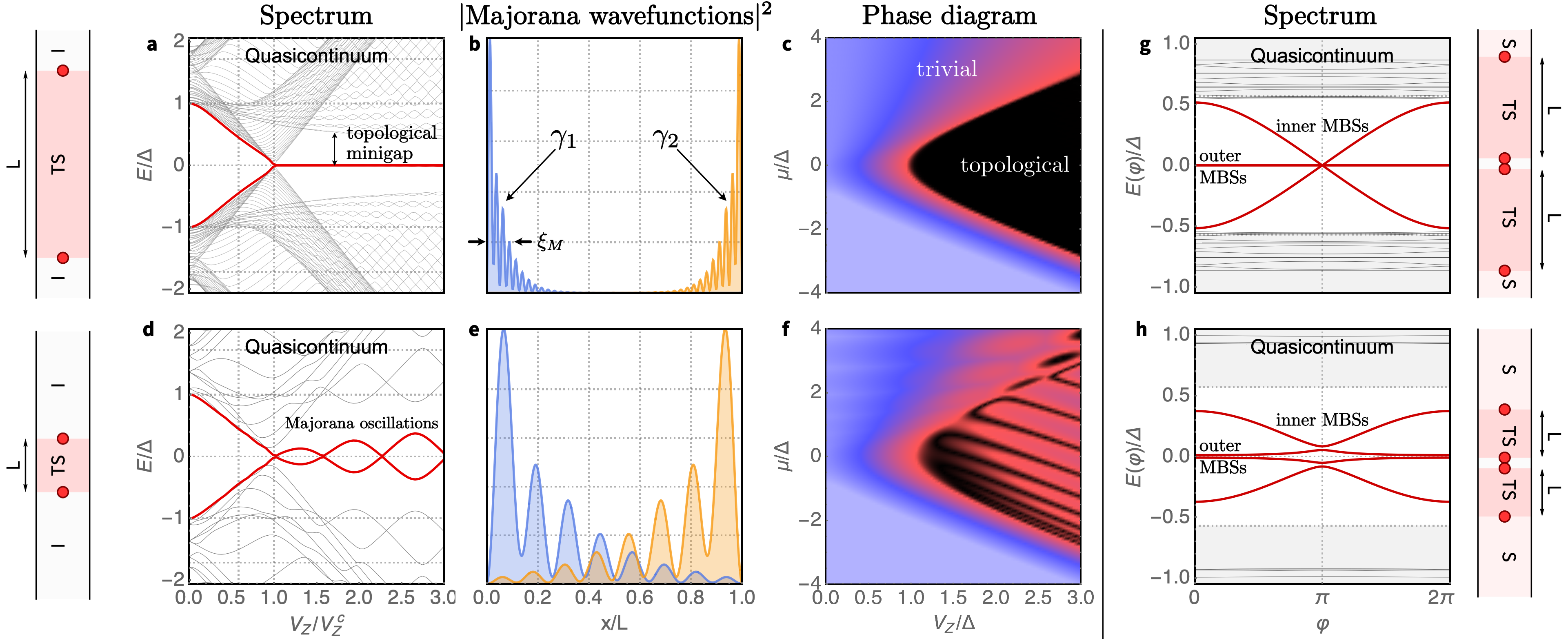
Figure 4 shows a complementary picture of the topological transition in a low-density, isolated ISI uniform nanowire of length (where stands for ‘insulator’), both in the long (a-c) and short (d-f) nanowire regime. As , a MBS appears localized at each end of the SC region, with zero energy in the large limit, or with characteristic Majorana oscillations around zero for shorter , resulting from their hybridization into conventional fermions due to their finite overlap. The lowest energy level [red in (a,d)] clearly traces the topological phase diagram for large , panel (c). It is interesting to note the role of finite in the topological Josephson effect [compare panels (g,h)]. Due to the overlap of the ‘inner’ MBSs in the junction and the ‘outer’ MBSs at the opposite ends of the nanowires, the Josephson periodicity is destroyed under an adiabatic , and a non-topological -periodic Josephson effect is restored Pikulin and Nazarov (2012); San-Jose et al. (2012). A similar effect is expected from quasiparticle poisoning (exchange of quasiparticles with the junction’s environment which breaks parity conservation) and by higher-energy quasiparticle excitation San-Jose et al. (2012).
The role of SO coupling is crucial for the physics of MBSs. For and larger than the spectrum is gapless (the magnetic field just kills superconductivity), so that no localized MBSs emerge, while for the system has a gap. The addition of SO coupling radically transforms this picture, and enables a topological minigap to emerge at . The minigap can be shown to be effectively -wave, and hence topologically non-trivial. The Majorana zero modes at the ends of a nanowire are in fact a manifestation of the bulk-boundary correspondence of this topological gap. They are thus topologically protected states. The extension of the Majorana wavefunction is the coherence length corresponding to the minigap (also known as the Majorana length Klinovaja and Loss (2012); Mishmash et al. (2016)) and is hence smaller for stronger SO coupling. The Majorana oscillatory hybridization is thus exponentially suppressed by both a strong SO (minigap) and nanowire length. In both limits, an exact Majorana topological protected zero mode is recovered at each end of the nanowire.
III.3 MBS spectroscopy
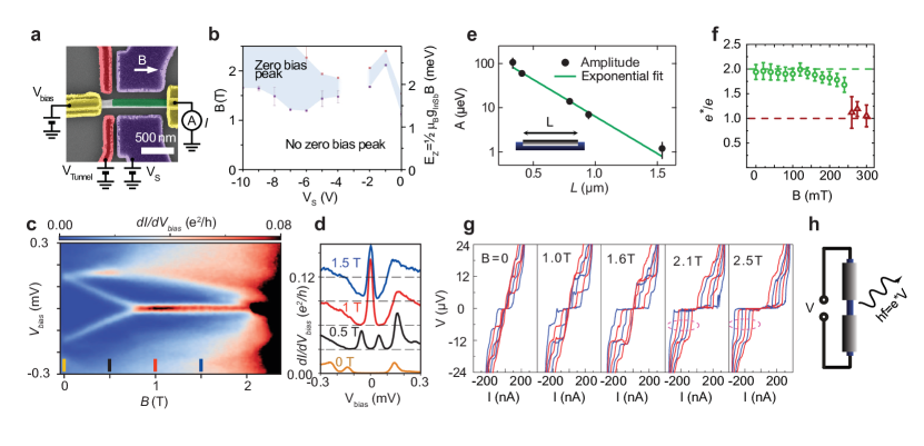
In this section, we outline the experimental techniques used to probe potential Majorana zero modes. First, tunneling spectroscopy as described in Sec. II.2 has been performed extensively in nanowires in devices of the kind shown in Fig. 5 (a), with the chemical potential in the nanowire controlled by the purple gate voltage . The gate-defined tunnel barrier (red gates) allows the conductance through the junction to probe the local density of states at the left end of the hybrid nanowire (green), typically exhibiting a roughly BCS-like gap [see the orange linecut in Fig. 5 (d)]. In these experiments Mourik et al. (2012); Das et al. (2012); Deng et al. (2016); Chen et al. (2017); Gül et al. (2018); Chen et al. (2019); Grivnin et al. (2019), the expected signature of a Majorana zero mode is a zero bias conductance peak above a threshold magnetic field [see Fig. 5 (c)], resulting from the resonant Andreev reflection on the MBS at the junction. This zero bias conductance peak is broadened due to both coupling to the normal lead (tunneling broadening ) and temperature (thermal broadening ). In the tunneling dominated regime , theory predicts that the peak should exhibit a universal quantized value of Law et al. (2009); Flensberg (2010); Wimmer et al. (2011). While most experiments yield much lower conductance values (see e.g. Fig. 5 (c,d) Deng et al. (2016)), consistent with the thermally broadened regime Prada et al. (2012); Setiawan et al. (2017), some experiments have reported scaling with the ratio and saturation values close to the ideal limit at low temperatures Nichele et al. (2017). Further comparison with theory [Fig. 4 (c)] can be performed by mapping the presence of the zero bias conductance peak as a function of the magnetic field and the gate voltage to create a phase diagram (see Fig. 5 (b) Chen et al. (2017); Gül et al. (2018)).
Another class of experiments targets superconducting islands, i.e., proximitized nanowires in a floating island geometry and characterized by combined superconducting and Coulomb blockade phenomenology. The Coulomb peak periodicity of the islands is found to transition from approximately - to -periodic under a finite Zeeman field due to the appearance of subgap near-zero modes Albrecht et al. (2016); Shen et al. (2018a); Vaitiekenas et al. (2020). The peak positions as a function of gate voltage show deviations from perfect periodicity, which are interpreted as energy splittings of the subgap states. The splittings were shown to oscillate around zero energy with Zeeman field, with an overall oscillation amplitude that decreases exponentially with increasing island length (Fig. 5 (e) Albrecht et al. (2016); Vaitiekenas et al. (2020)). The oscillations and their cutoff length nm have been interpreted as resulting from Majorana splittings, see Fig. 4 (b,e).
Apart from tunneling spectroscopy measurements, in order to detect MBSs one can also explore dynamical detection techniques in SNS junctions. In Sec. II.1 we discussed the ABS spectrum and concluded that in a finite-transparency, high-density, short junction, they exhibit an avoided crossing at , while in Sec. III.2 we saw that in the topological phase, has a protected crossing at , leading to the -periodic Josephson effect. At first glance, a tempting experimental detection of the topological Josephson junction is to directly measure the gapless nature of the ABSs, , or the corresponding current-phase relation, . However, as mentioned in the preceding section, in a finite length system of length , the overlap between the ‘inner’ and ‘outer’ Majorana wavefunctions restores the avoided crossing with an energy scale van Heck et al. (2011); Pikulin and Nazarov (2012); San-Jose et al. (2012). In addition, the tunneling of unpaired non-equilibrium quasiparticles enables relaxation to the parity ground state, resulting in a trivial, -periodic behavior on timescales much longer than the parity poisoning time of the system Lutchyn et al. (2010); Houzet et al. (2013).
Due to these challenges, the experimental detection efforts of the -periodic Andreev levels have typically focused on dynamical detection techniques based on the ac Josephson effect Josephson (1962), Fig. 5 (h). In conventional -periodic Josephson junctions in the tunneling limit a junction bias produces an oscillating supercurrent , with V Parker et al. (1967). In the topological Josephson effect, the -periodicity of subgap states translate into a halving of the frequency . This halving becomes visible in Shapiro step measurements Shapiro (1963), where the junction is irradiated at a frequency in the microwave domain. The dc component of develops discrete voltage steps with a spacing of and for the trivial and topological state, respectively Domínguez et al. (2012); Houzet et al. (2013); Sau and Setiawan (2017). While the disappearance of the first voltage step was repeatedly observed, Fig. 5 (g), higher odd steps typically persist in experiments Rokhinson et al. (2012); Kamata et al. (2018). It has been argued that the interpretation of the measurements needs to include the deviations from the tunnel junction behavior, such as non-sinusoidal supercurrents Domínguez et al. (2012), overheating effects De Cecco et al. (2016); Le Calvez et al. (2019), capacitive shunting Picó-Cortés et al. (2017), Landau-Zener tunneling between the Andreev bands and to the quasiparticle continuum Pikulin and Nazarov (2012); Sau and Setiawan (2017); Virtanen and Recher (2013). Furthermore, the addition of several non-topological ABSs has a non-trivial effect on the observed Shapiro steps Domínguez et al. (2012, 2017b).
Another class of experiments rely on the direct spectroscopical detection of the Josephson radiation of voltage-biased junctions, which is expected to be centered at or at San-Jose et al. (2012). This transition has been observed in InAs/Al nanowire Josephson junctions integrated with an on-chip SIS microwave detector (Fig. 5 (f), Laroche et al. (2019)), and by using a conventional microwave amplifier chain Kamata et al. (2018).
It should be noted that additional measurement schemes were proposed to observe the -periodic Josephson effects as a probe for topological superconductivity. These utilize Shapiro steps in the low-frequency regime Sau and Setiawan (2017), Andreev level pair excitations in long junctions Väyrynen et al. (2015), critical current measurements San-Jose et al. (2014); Tiira et al. (2017); Cayao et al. (2017), or the shape of switching current histograms Peng et al. (2016).
IV MBSs beyond the minimal model
IV.1 Extensions of the minimal model
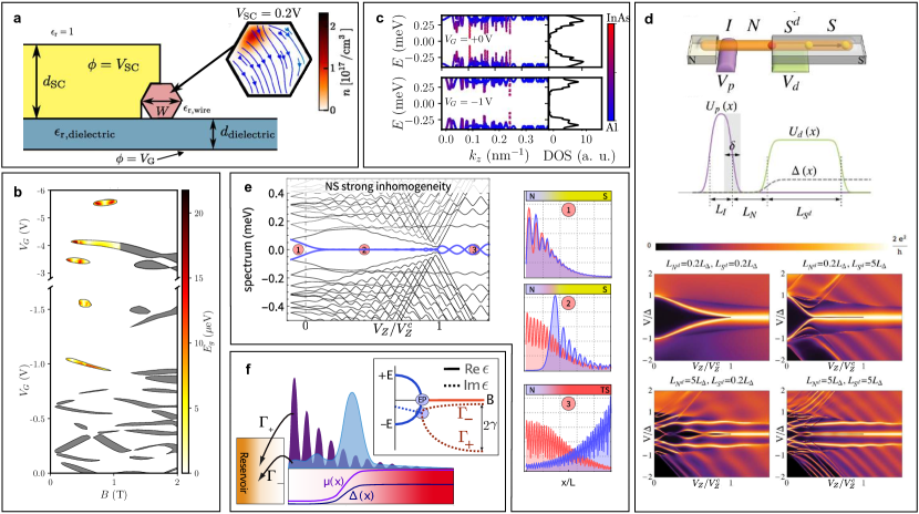
The minimal Oreg-Lutchyn model has proven to be a first useful guide to investigate the physics of Majorana nanowires. However, discrepancies between its predictions and experimental observations have motivated extensions that provide a more complete understanding of the experimental system. A natural extension of the 1D single band model is to allow for multiple subbands in the nanowire Potter and Lee (2010, 2011); Lutchyn et al. (2011); Lutchyn and Fisher (2011). This results in a more complicated phase diagram, depending on the number of occupied bands and their relative energies. Additionally, the orbital effects of the magnetic field (i.e. the magnetic flux across the nanowire section) may become relevant, especially when the number of occupied subbands is increased Nijholt and Akhmerov (2016). They have been shown to dramatically modify the topological phase diagram Nijholt and Akhmerov (2016); Winkler et al. (2019) [see Fig. 6 (b)] and the dispersion of states in the nanowire, leading to large effective -factors Nilsson et al. (2009); Winkler et al. (2017) and suppressed topological gaps Nijholt and Akhmerov (2016). Although numerical simulations of multiband wires can shed additional light on the experimental results, they tend to depend strongly on details such as the geometry and effective parameter values which are not always experimentally accessible.
While initial experiments generally suffered from unwanted quasiparticle states inside the superconducting gap [referred to as “soft gap” Mourik et al. (2012); Takei et al. (2013); Winkler et al. (2019), see Fig. 6 (c)], clean superconducting gaps comparable to the bulk gap of the parent SC have since been achieved Chang et al. (2015); Zhang et al. (2017) by engineering epitaxial interfaces between the two material systems Krogstrup et al. (2015); Gazibegovic et al. (2017). Both the “soft gap” issue Stanescu and Tewari (2013b) and the large gaps measured in later experiments ignited interest in a more complete description of the superconducting proximity effect in these systems. This includes pair breaking effects that suppress superconductivity beyond a critical value of the magnetic field, or a more accurate model for the induced pairing in the form of an energy-dependent anomalous self-energy. The latter extends the regime of weak coupling between the semiconductor and the SC, wherein the induced superconducting gap is simply proportional to the coupling strength between the two systems. It was found that in the opposite, strong coupling regime, the band structure of the nanowire is significantly altered, resulting in a strong renormalization of model parameters Cole et al. (2015). It has also been demonstrated that the proximity effect can strongly depend on the thickness of the SC film Reeg et al. (2017, 2018a); Awoga et al. (2019). The SC-semiconductor coupling has furthermore been found to depend on the details of the electrostatic environment Antipov et al. (2018); Mikkelsen et al. (2018), resulting in gate voltage dependent effective parameters such as the -factor Vaitiekenas et al. (2018); Pan et al. (2019), the SO coupling Escribano et al. (2020) and the induced gap de Moor et al. (2018).
A notable disagreement between most experiments and the minimal model revolves around the Majorana oscillations. The oscillatory energy splittings are predicted to be regular and grow with Zeeman field Lim et al. (2012); Prada et al. (2012); Das Sarma et al. (2012); Rainis et al. (2013); Sharma et al. (2020), while in most experiments robust zero-bias peaks appear without oscillations Deng et al. (2016); Zhang et al. (2017). Several model extensions have been explored that predict a reduction or suppression of oscillations, such as interactions with a dielectric environment or among carriers Das Sarma et al. (2012); Domínguez et al. (2017a); Escribano et al. (2018), orbital effects Dmytruk and Klinovaja (2018), dissipation Liu et al. (2017b); Danon et al. (2017); Avila et al. (2019) or non-uniform potentials Peñaranda et al. (2018); Sharma et al. (2020), pairing Fleckenstein et al. (2018) or SO coupling Cao et al. (2019). A further common disagreement is a lack of visible bandgap-closing and reopening in some experiments Mourik et al. (2012); Deng et al. (2016); Vaitiekenas et al. (2018), which is a key feature of the model’s topological transition. This has been explained as the result of poor visibility resulting from tunnel probe smoothness Prada et al. (2012); Stanescu et al. (2012) and even by a lack of bulk transition altogether Huang et al. (2018), as will be discussed in Sec. IV.3.
The topological phase transitions in these extended models are generally calculated using the chemical potential and the Zeeman energy . However, the control parameters used in experiments are gate voltages and magnetic fields. Calculating the phase diagram in terms of gate voltages requires a self-consistent treatment of the electrostatics Vuik et al. (2016). While some progress has been made in self-consistent Schrödinger-Poisson calculation for 3D device geometries Woods et al. (2018); Antipov et al. (2018); Escribano et al. (2018); Winkler et al. (2019) [see Fig. 6 (a)], this remains a difficult problem to solve reliably. In addition to electrostatic modifications of the phase diagram, interaction effects have been demonstrated to play a role in the low energy spectrum of Majorana nanowires Vuik et al. (2016); Domínguez et al. (2017a); Escribano et al. (2018).
An immediate effect of a self-consistent description of nanowire junctions, both for electrostatics and the proximity effect, is a smoothening of the pairing and Fermi energy profiles Prada et al. (2012), which can no longer be assumed piecewise-constant as in the minimal model. Smooth , at a junction have been shown to give rise to near-zero modes without the need of a topological bulk. We devote the next subsections to these and other types of non-topological zero modes.
![[Uncaptioned image]](/html/1911.04512/assets/x5.png)
IV.2 Zero energy pinning with a topologically trivial bulk
The combination of multiband wires with disorder has been shown Bagrets and Altland (2012); Rainis et al. (2013); Beenakker (2015) to produce topologically trivial zero energy states in class D Hamiltonians Altland and Zirnbauer (1997); Schnyder et al. (2008). Since the advent of cleaner experiments, it has become possible to distinguish disorder-based mechanisms from zero bias peaks of different origin, as the former are associated to specific observable features (e.g. soft gap, low transport peak heights) that have been optimized away. Strong interband coupling in multimode clean wires with a single short-range potential inhomogeneity have also been shown to conspire to produce approximate zero energy states of non-topological states Woods et al. (2019); Chen et al. (2019).
Near-zero bound states can also be generically present in a tunneling spectroscopy nanowire setup if there is a non-superconducting section between the tunnel barrier and the superconducting wire Prada et al. (2012); Chevallier et al. (2012); Cayao et al. (2015); Liu et al. (2017a); Ptok et al. (2017); Moore et al. (2018b); Peñaranda et al. (2018); Reeg et al. (2018a, b); Vuik et al. (2019); Avila et al. (2019); Stanescu and Tewari (2019) [Fig. 6 (d)]. Such an N region can host ABSs that become spin-polarized under a Zeeman field and may thus be tuned to zero energy, much like the Shiba states, possibly with a strongly renormalized -factor due to SO coupling Dmytruk et al. (2018). In the simplest situation, these are readily distinguished because their zero energy results from fine tuning parameters such as to specific values, unlike for topological MBSs. Under some circumstances, however, these modes can become pinned to zero or near-zero energy for an extended range in magnetic field and other control parameters, resembling the behavior expected from MBSs, but with the SC in the topologically trivial phase Prada et al. (2012); Kells et al. (2012); Stanescu and Tewari (2013b); Liu et al. (2017a); Moore et al. (2018a); Peñaranda et al. (2018); Reeg et al. (2018b); Liu et al. (2018); Moore et al. (2018b); Vuik et al. (2019); Avila et al. (2019); Stanescu and Tewari (2019).
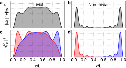
In the case of isolated NS nanowire junctions, we can distinguish two main mechanisms for zero-energy pinning of a non-topological zero mode: smooth confinement Moore et al. (2018a); Peñaranda et al. (2018); Vuik et al. (2019); Avila et al. (2019); Stanescu and Tewari (2019) and SO-induced pinning Reeg et al. (2018b). Both effects ultimately cause an enhanced Andreev reflection of a normal electron on the trivial SC. In the case of a junction with spatially smooth parameters, the momentum transfer required for normal reflection at the junction is suppressed, and hence Andreev reflection dominates. Under these conditions, states at the junctions decouple into two sectors around different Fermi wavevector and spin (due to the SO coupling and the Zeeman field) Kells et al. (2012); Vuik et al. (2019); Peñaranda et al. (2018), each of which behaves as an independent topological -wave SC that gives rise to a zero-energy MBS decoupled from its partner. The Majorana wavefunction corresponding to the two wavevectors are centered at different positions along the wire and exhibit different spatial profiles (oscillatory exponential and smooth gaussian, respectively Peñaranda et al. (2018); Stanescu and Tewari (2019)), see Fig. 6 (e).
A similar pinning effect can be caused by SO coupling. For large SO, the effective -factor is strongly renormalized and ABSs can become largely insensitive to magnetic fields Dmytruk et al. (2018). When the length of the N section is further tuned to an approximately odd-integer multiple of the SO length, an ABS will appear pinned near zero energy respect to Reeg et al. (2018b). This SO-induced pinning does not require junction smoothness, but the above Fabry-Perot resonance condition on length must be satisfied.
A third route towards stabilising zero modes belonging to a nominally trivial bulk has been proposed in topologically trivial nanowires open to fermion reservoirs (which is a standard geometry in NS junctions used to perform transport spectroscopy). When such a nanowire becomes coupled to the reservoir, it can develop an ‘exceptional point’ (EP) bifurcation in its complex (non-Hermitian) spectrum, see Fig. 6 (f), where the real part of the lowest quasibound Bogoliubov mode becomes robustly pinned to zero energy as the imaginary part bifurcates. This kind of non-Hermitian topological transition stabilizes a couple of quasibound states at the contact with different decay rates. One of the two may become essentially non-decaying after the exceptional point bifurcation, thus becoming a stable Majorana zero mode without the need of a bulk topological transition. An EP requires a finite coupling asymmetry of the two Majorana components to the reservoir. Sources of asymmetry include finite length Pikulin and Nazarov (2013); Avila et al. (2019), smooth potentials Avila et al. (2019), spin-polarized leads San-Jose et al. (2016), etc. Research into Majorana states in open systems for quantum computation purposes is still in its early stages. The field is advancing rapidly, however, with e.g. new non-Hermitian topological classification theories being developed recently Leykam et al. (2017); Shen et al. (2018b); Gong et al. (2018); McGinley and Cooper (2019) that extend band-topological concepts to open systems where these do not strictly apply.
IV.3 The MBS vs. ABS controversy
As studies began to unveil the above phenomenology beyond the minimal model, it became clear that many experimental hints of Majoranas could easily be mistaking zero modes of non-topological origin with MBSs resulting from a non-trivial bulk topology. Notable examples include experiments showing zero bias peaks robust against magnetic field variations, or even conductance values close to the ideal quantized value. Until recently, both cases were considered strong signatures of emergent Majoranas after a bulk topological transition, but a growing body of literature shows that this is not necessarily the case Moore et al. (2018b); Vuik et al. (2019); Avila et al. (2019); Stanescu and Tewari (2019); Yu et al. (2020). A prominent reason is the possibility of robust but trivial zero modes arising at smooth inhomogeneities Prada et al. (2012); Kells et al. (2012); Stanescu and Tewari (2013b); Roy et al. (2013); Stanescu and Tewari (2014); Liu et al. (2017a); Fleckenstein et al. (2018); Peñaranda et al. (2018); Reeg et al. (2018b); Liu et al. (2018); Moore et al. (2018a, b); Vuik et al. (2019); Avila et al. (2019); Stanescu and Tewari (2019). Instead of emerging from a band inversion at a critical , these subgap states are predicted to emerge as a lone ABS that detaches from the continuum as increases, and gradually becomes pinned to zero energy with no intervening bulk topological transition or band inversion Prada et al. (2012); Szumniak et al. (2017); Peñaranda et al. (2018); Moore et al. (2018a); Vuik et al. (2019), see Fig. 6 (d). This telltale feature is often observed in experiments, see e.g. Fig. 5 (c), and should be taken as a strong hint that the zero mode might not be the result of an underlying bulk topological transition. This type of zero mode has been dubbed a quasi-MBS Vuik et al. (2019), partially-separated MBS (ps-MBS) Moore et al. (2018a), or non-topological MBS Avila et al. (2019). Notably, these states are not localized at opposite edges of the nanowire but are instead confined to the inhomogeneity neighborhood, whose location is often uncontrolled. As shown in Fig. 6 (e), subpanel 2, they typically exhibit a substantial spatial overlap.
Quasi-MBSs could also complicate the interpretation of superconducting Coulomb islands experiments Albrecht et al. (2016); Shen et al. (2018a); Vaitiekenas et al. (2020). The Coulomb peak spacing technique used there allows to extract the energy splitting of nanowire zero-bias anomalies with high precision, see Sec. LABEL:sec:MBSspec. These measurements show oscillatory splittings that decay exponentially with nanowire length. The decay is compatible with MBSs spatially separated by a gapped topological bulk, see Fig. 5 (e). However, the observations may also be compatible with pairs of quasi-MBSs, as the splittings of the latter can become exponentially suppressed due to reasons other than spatial separation 111As nanowire screening lengths are often in the hundreds of nanometers, it is plausible to expect smoother confinement potentials, and hence suppressed splittings, as the nanowire length is increased. The oscillations, moreover, are found to decay with magnetic field, contrary to the behaviour expected from topological MBSs Chiu et al. (2017), and more in line with that of quasi-MBSs.
This kind of interpretation loophole is likely unavoidable in almost any type of experiment using purely local probes, which explains the longevity of the MBS vs ABS controversy. Other than finding a quantitative match with theoretical models across a large portion of parameter space, it seems that the only way out of these ambiguities will require truly non-local experimental schemes, see Sec. IV.4. In view of this, it becomes crucial to consider all possible types of zero modes when interpreting current and future experiments.
A summary of the main types of zero modes and their defining properties is given in Table 1. We distinguish broadly between (a) conventional, topologically trivial ABSs and variations thereof, (b) MBSs of topological origin, and (c) zero modes produced by some form of smooth inhomogeneity with a trivial bulk. The first group includes the SNS ABSs of Figs. 1 and 3 (e-g), with or without SO coupling and Zeeman field. These states can be fine-tuned to zero energy by e.g a phase difference across the junction or an adequate Zeeman field . The analogous ABSs in INS junctions, magnetic impurities or proximitized quantum dots are grouped under Shiba states, see Fig. 2 (g). ABSs usually show no pinning to zero energy. However, ABSs INS junctions with strong SO coupling Reeg et al. (2018b) or with short-range inhomogeneities and interband coupling Woods et al. (2019); Chen et al. (2019) may exhibit approximate zero-energy pinning as a function of some system parameters, as mentioned in Sec. IV.2. In general all these ABSs have a high degree of spatial overlap of their Majorana components. In the second group we consider the topological MBSs in nanowires with a topological bulk, both for short and long nanowires. The latter case corresponds to MBSs with exponentially small overlaps, the paradigmatic case highlighted by minimal models. In the last group we include all zero modes produced by sufficiently smooth inhomogeneities. We distinguish states in smoothly confined SC nanowires Kells et al. (2012) and the various forms of topologically trivial zero modes in smooth NS or S’S junctions Prada et al. (2012); Stanescu and Tewari (2013b); Roy et al. (2013); Stanescu and Tewari (2014); Liu et al. (2017a); Fleckenstein et al. (2018); Peñaranda et al. (2018); Reeg et al. (2018b); Liu et al. (2018); Moore et al. (2018a, b); Vuik et al. (2019); Stanescu and Tewari (2019), including the exceptional point MBS (EP-MBS) generalization in open systems San-Jose et al. (2016); Avila et al. (2019). The distinction between these subclasses is mostly historical, however, as the underlying mechanism for their formation is the same. All these states are characterized by a strong pinning as smoothness is increased, and partially overlapping wavefunctions.
The debate on the interpretation of experimental signatures has often been framed in terms of “true” and “fake” MBSs, or actual MBSs (of the topological class above) and conventional zero energy ABSs. Such dichotomy has had the unfortunate side effect of establishing an imprecise terminology in some of the literature, whereby the term “Majorana” is used as a synonym of non-trivial band topology, instead of its original meaning of a self-conjugate zero-energy eigenstate. In truth, any zero energy fermionic eigenstate of a hybrid system, regardless of its origin, can be formally expressed as the sum of two self-conjugate Majorana eigenstates Kitaev (2001), see Box. B. This includes zero-energy trivial-bulk quasi- or ps-MBSs.
As we expand upon in the next section, what makes MBSs of topological origin special is the exponential suppression of the spatial overlap between the and wavefunctions (i.e. the degree of non-locality of ). This suppression, however, requires nanowires longer than the Majorana length, , and of sufficiently uniformity so that MBSs are truly located at their ends (i.e. no additional zero modes appear in the bulk at uncontrolled inhomogeneities or defects). In real, finite-length nanowires these stringent conditions need not be satisfied. In a generic case, a useful formulation of the MBSs vs ABSs debate is based on whether a given robust zero-energy mode, regardless of its trivial or non-trivial bulk topology, has a sufficiently small Majorana overlap for a given application. Some requirements, such as resilience to arbitrary local noise or the possibility of spatial braiding, demand exponentially suppressed overlaps, while others, such as parametric non-Abelian braiding (i.e. relative phase manipulations without spatial displacements), merely need that a local probe may be selectively coupled to a single Majorana Vuik et al. (2019); San-Jose et al. (2016); Avila et al. (2019). In such cases, ps-MBSs may be good enough.
IV.4 Protection against errors and MBS overlaps
Topological quantum computation was proposed as a way to achieve scalability through the hardware-level resilience of Majorana-based qubits to arbitrary local noise, in principle guaranteed by spatial non-locality. The Majorana qubit is defined in terms of the occupation of non-local fermion states such as Kitaev (2001), see Box B. As efforts develop towards realising this promise, different error-inducing mechanisms have been identified and studied for topological MBS qubits, such as those created by a coupling to ungapped Budich et al. (2012) or gapped Goldstein and Chamon (2011); Rainis and Loss (2012) fermionic baths (quasiparticle poisoning), as well as to fluctuating bosonic fields Pedrocchi and DiVincenzo (2015) (e.g. phonons Knapp et al. (2018); Aseev et al. (2019), photons Trif and Tserkovnyak (2012); Schmidt et al. (2013); Dmytruk et al. (2015), thermal fluctuations of a gate potential Aseev et al. (2018); Schmidt et al. (2012); Lai et al. (2018), or electromagnetic environments Knapp et al. (2018)). One must also consider the errors induced by qubit manipulation, such as unwanted excitations created by nonadiabatic manipulation Scheurer and Shnirman (2013); Sekania et al. (2017), which are largely controlled by the superconducting minigap.
Given the likely ubiquity of non-topological zero modes in realistic devices Chen et al. (2019), particularly when including QDs and screened barriers as basic elements of many proposed schemes for topological quantum computing Hoffman et al. (2016); Wakatsuki et al. (2014); Karzig et al. (2017); Plugge et al. (2017), it has become important to understand whether the protection of topological MBSs applies in some form also to non-topological zero modes. A precise answer requires quantifying the Majorana overlap of a given zero mode in a sample. Traditional experimental schemes to measure the subgap spectrum of nanowires, such as tunneling spectroscopy, rely on local probes, so that they do not directly access the degree of non-locality of a given zero bias anomaly. An alternative, though still local scheme has been proposed to extract a quantitative estimate of the degree of MBS overlap Prada et al. (2017); Clarke (2017); Schuray et al. (2017); Peñaranda et al. (2018). It consists of measuring tunneling spectroscopy into the end of the nanowire through a QD in series, which reveals the asymmetric coupling of spin-polarized states in the QD with the two spatially separated Majorana components of the zero mode. Such a scheme was implemented in a recent experiment Deng et al. (2018) that demonstrated a varying degree of wavefunction overlap in otherwise similar zero modes. Multiple tunnel probes have also been employed recently in search of clearer and less ambiguous evidence of zero-mode non-locality and non-trivial topology Grivnin et al. (2019); Anselmetti et al. (2019); Ménard et al. (2020); Puglia et al. (2020).
V Summary and outlook
We have reviewed the remarkable advances towards characterizing the detailed structure of ABSs in hybrid nanowires with strong SO coupling, and related systems. In ideal nanowires, ABSs evolve with magnetic fields and gates, developing a spatial separation of their wavefunction components and ultimately transforming into robust, non-local, topological Majorana zero energy modes beyond a critical Zeeman field. Experimental observations, however, deviate from the predictions of minimal models, making evident the need to incorporate extensions, such as the electrostatic environment, multimode and orbital effects, spatial inhomogeneities and momentum mixing. These additions introduce a complex, non-universal phenomenology. Theoretical work has identified alternative routes towards stabilizing zero modes, different from a bulk topological phase transition. Such routes include using smooth and/or spin-dependent confinement, or exceptional point bifurcations in open (non-Hermitian) systems. However, the wavefunction non-locality obtained by such means is generally poor. Given the importance of non-locality for the protection of MBSs, their resilience against noise and the possibility of carrying out braiding operations on them, it has become a major focus point in current experiments to detect and quantify the degree of Majorana overlap. First results in this area have been obtained using purely local probes. These have intrinsic limitations, unfortunately, and can only suggest, not demonstrate, Majorana non-locality. Experiments are underway, nevertheless, to exploit truly non-local measurements in more complex nanowire setups without such limitations Zhang et al. (2019); Frolov et al. (2020); Aguado and Kouwenhoven (2020). The ultimate demonstration, non-Abelian braiding, remains an open challenge.
Nonlocality and braiding are the cornerstones behind the original promise of Majorana applications, namely, to harness the hardware-level resilience of Majorana qubits to solve the scalability problem of quantum computers. This is an ambitious long-term endeavour that will require solving important challenges to finally bring Majoranas out of the lab. Majorana nanowires will likely have an important role in this journey, as they represent the most readily accessible system of this kind and the most explored topological superconductor so far. However, they also have some disadvantages such as the unwanted presence of nontopological in-gap states or the necessity to subject the wire to strong magnetic fields. So far, partially-covered nanowires have been intensively explored, but other alternatives with some interesting advantages are beginning to be studied, such as full-shell nanowires Vaitiekenas et al. (2020); Peñaranda et al. (2020) and ferromagnetic hybrid structures Vaitiekėnas et al. (2020). Additionally, the recent demonstration of gate-tunable nanowire-based superconducting qubits, so-called gatemons Larsen et al. (2015); de Lange et al. (2015), which include full-shell nanowires Sabonis et al. (2020) and junctions with quantum dots Bargerbos et al. (2020); Kringhøj et al. (2020), opens new possibilities for studying Majorana physics in hybrid architectures that use more mature technologies such as circuit QED and transmon qubits Ginossar and Grosfeld (2014); Trif et al. (2018); Keselman et al. (2019); Avila et al. (2020a, b).
Nevertheless, it is entirely possible that radically different Majorana platforms will be discovered that exhibit cleaner and larger gaps, improved Majorana non-locality, easier braiding, and crucially, are more amenable to scalable fabrication and integration. Leading explorations include experiments on shallow quantum wells that can be proximitized by epitaxial superconductors, while being compatible with lithographic patterning techniques Suominen et al. (2017). On such platforms crossed-Andreev reflection has been proposed as an alternative way to stabilize Majoranas Finocchiaro et al. (2018); Thakurathi et al. (2018). Also, the use of two-dimensional van der Waals crystals has received attention recently Young et al. (2014); Lee et al. (2017b), where the SO coupling, required for generating MBSs, could be replaced by carrier chirality and intrinsic interactions San-Jose et al. (2015). Solving the material-science side of the challenge is crucial before tackling the more applied problems of engineering, operating and integrating coherent ensembles of topological quantum gates. We expect these efforts to continue fertilizing condensed-matter research with novel and exciting possibilities.
VI Author contributions
L. P. K. initiated this review and E. P. coordinated the project. All authors discussed the general structure of the manuscript. M. W. A. M. and A. G. wrote “ABS spectroscopy”, “MBS spectroscopy” and contributed to “Extensions of the minimal model”. E. J. H. L., J. N. and R. A. wrote “ABSs in QDs”. J. K. and D. L. contributed to “Zero-energy pinning with a topologically trivial bulk” and ‘Protection against errors and MBS overlaps”. E. P., P. S.-J. and R. A. wrote everything else. All authors reviewed and polished the manuscript.
Acknowledgements.
Research supported by the Spanish Ministry of Science, Innovation and Universities through grants FIS2015-65706-P, FIS2015-64654-P, FIS2016-80434-P, FIS2017-84860-R, PCI2018-093026 and PGC2018-097018-B-I00 (AEI/FEDER, EU), the Ramón y Cajal programme grant RYC-2011-09345 and RYC-2015-17973, the María de Maeztu Programme for Units of Excellence in R&D (MDM-2014-0377), the European Union’s Horizon 2020 research and innovation programme under grant agreements Nos 828948 (FETOPEN AndQC), 127900 (Quantera SuperTOP), the European Research Council (ERC) Starting Grant agreements 716559 (TOPOQDot), 757725 (ETOPEX) and 804988 (SiMS), the Netherlands Organization for Scientific Research (NWO), Microsoft, the Danish National Research Foundation, the Carlsberg Foundation, and the Swiss National Science Foundation and NCCR QSIT. We also acknowledge support from CSIC Research Platform on Quantum Technologies PTI-001.Appendix A Box A – Proximitized nanowire model
The starting point of the proximitized nanowire model (R. M. Lutchyn et al Lutchyn et al. (2010) and Y. Oreg et al Oreg et al. (2010)) is a Hamiltonian describing a 1D semiconducting nanowire with Rashba spin-orbit (SO) interaction and in the presence of an external magnetic field perpendicular to the Rashba field (here, we assume that is applied parallel to the nanowire axis ):
with
| (6) |
where is the effective mass of the semiconductor, its chemical potential, the SO coupling and the Zeeman energy produced by , given in terms of the nanowire’s -factor (with being the Bohr’s magneton). are Nambu spinors and and Pauli matrices in spin and particle-hole space, respectively.
Solving the above Hamiltonian in reciprocal space yields a dispersion relation of the form . In the absence of Zeeman field, , the Rashba term removes the spin degeneracy of the 1D parabolic band and gives rise to two parabolas shifted relative to each other along the momentum axis (each by an amount ) and displaced down in energy by an amount , where the reduced Planck’s constant, see Fig. 7 (a). These parabolas correspond to spin up and spin down projections along the spin-quantization axis fixed by the Rashba coupling (here ). On the other hand, a finite Zeeman mixes both spins and hence removes the spin degeneracy at by opening up a gap of size , Fig. 7 (b). These split bands define two sectors + and - of opposite helicity at large and small momenta, respectively. If , only the + sector is present around the Fermi energy (helical regime). Projecting a standard -wave pairing term onto the helical basis one obtains intraband (spinless) pairing terms of the form , with having so-called -wave symmetry . In the helical regime, the minimal Hamiltonian is thus a realistic implementation of the Kitaev model for 1D -wave superconductivity Kitaev (2001). When the applied Zeeman field is larger than the critical value , the 1D SC becomes topological and hosts MBSs at its ends.
To implement this proposal in experimentally realizable systems, one needs semiconductors with large -factors in order to achieve a large under moderate external magnetic fields below the critical field of the SC. A good proximity effect with conventional SCs and a large Rashba energy are also necessary. Last but not least, one needs to be able to keep the chemical potential of the nanowire close to zero (in order to reach the helical regime with spin-momentum locking for moderate ), despite the proximity to the SC.
Appendix B Box B – Majorana basis
A Bogoliubov-de Gennes eigenstate in a superconducting system is an excitation of energy over its ground state that consists of a superposition of one electron and one hole quasiparticles,
Here and create and destroy a quasiparticle of spin perfectly localized at point , respectively, and are electron/hole wavefunctions.
If the energy of a given eigenstate becomes negligibly small as in the case of a topological Majorana nanowire, the eigenstates and are both degenerate ground states, of even and odd fermionic parity, respectively. If we denote and , we find that and switch between the two
The matrix elements of in this subspace are therefore and , where are Pauli matrices.
By performing a unitary rotation to the so-called Majorana basis, the eigenstate operators can be decomposed into two Majorana operators that satisfy self-conjugation, and , so that
| (7) |
Each Majorana operator corresponds to a fermionic eigenstate, in the sense that , but the Majorana reality property also implies that, unlike a conventional fermion, . The matrix elements of in the ground state subspace are .
The Majorana states created by and are sometimes intuitively described as half-fermions, as they always come in pairs and any two in a system can be combined to create a conventional fermion as above. In a topological Majorana nanowire, the wavefunction of
is localized at either end of the nanowire, unlike of , that occupies both ends, see Fig. 8. The latter is hence called a non-local fermion.
The above transformations, Eqs. (7), can be applied to an arbitrary ABS of finite energy. In such case, the resulting Majorana states are not eigenstates. However, the decomposition still allows to examine the degree of Majorana non-locality of by computing the overlap between the corresponding and .
References
- Kamerlingh Onnes (1911) H. Kamerlingh Onnes, Comm. Phys. Lab. Univ. Leiden 122, 122 (1911).
- van Delft and Kes (2010) D. van Delft and P. Kes, Phys. Today 63, 38 (2010).
- De Gennes (2018) P.-G. De Gennes, Superconductivity of metals and alloys (CRC Press, 2018).
- Tinkham (2004) M. Tinkham, Introduction to superconductivity (Courier Corporation, 2004).
- Martin (2019) J. D. Martin, Phys. Today 72, 30 (2019).
- Bardeen et al. (1957) J. Bardeen, L. N. Cooper, and J. R. Schrieffer, Phys. Rev. 106, 162 (1957).
- Cooper (1956) L. N. Cooper, Phys. Rev. 104, 1189 (1956).
- Ginzburg and Landau (1950) V. L. Ginzburg and L. D. Landau, Zh. Eksp. Teor. Fiz. 20, 1064 (1950).
- Cyrot (1973) M. Cyrot, Rep. Prog. Phys. 36, 103 (1973).
- Caroli et al. (1964) C. Caroli, P. D. Gennes, and J. Matricon, Phys. Lett. 9, 307 (1964).
- Yu (1965) L. Yu, Acta. Phys. Sin. 21, 75 (1965).
- Shiba (1968) H. Shiba, Prog. Theor. Phys. 40, 435 (1968).
- Rusinov (1969) A. Rusinov, Sov. Phys. JETP 9, 85 (1969).
- Blonder et al. (1982) G. E. Blonder, M. Tinkham, and T. M. Klapwijk, Phys. Rev. B 25, 4515 (1982).
- Andreev (1964) A. F. Andreev, Sov. Phys. JETP 19, 1228 (1964).
- Andreev (1966) A. F. Andreev, Sov. Phys. JETP 22, 18 (1966).
- De Gennes and Saint-James (1963) P. De Gennes and D. Saint-James, Phys. Lett. 4 (1963).
- Kulik (1970) I. O. Kulik, Sov. Phys. JETP 30, 944 (1970).
- Sauls (2018) J. A. Sauls, Philos. Trans. Royal Soc. A 376 (2018).
- Hasan and Kane (2010) M. Z. Hasan and C. L. Kane, Rev. Mod. Phys. 82, 3045 (2010).
- Qi and Zhang (2011) X.-L. Qi and S.-C. Zhang, Rev. Mod. Phys. 83, 1057 (2011).
- Thouless et al. (1982) D. J. Thouless, M. Kohmoto, M. P. Nightingale, and M. den Nijs, Phys. Rev. Lett. 49, 405 (1982).
- Leijnse and Flensberg (2012) M. Leijnse and K. Flensberg, Semicond. Sci. Technol. 27, 124003 (2012).
- Alicea (2012) J. Alicea, Rep. Prog. Phys. 75, 076501 (2012).
- Beenakker (2013) C. Beenakker, Annu. Rev. Cond. Mat. Phys. 4, 113 (2013).
- Sato and Fujimoto (2016) M. Sato and S. Fujimoto, J. Phys. Soc. Jpn 85, 072001 (2016).
- Aguado (2017) R. Aguado, Riv. Nuovo Cimento 40, 523 (2017).
- Sato and Ando (2017) M. Sato and Y. Ando, Rep. Prog. Phys. 80, 076501 (2017).
- Salomaa and Volovik (1988) M. Salomaa and G. Volovik, Phys. Rev. B 37, 9298 (1988).
- Volovik and Volovik (2009) G. E. Volovik and G. Volovik, The universe in a helium droplet, Vol. 117 (Oxford University Press New York, 2009).
- Read and Green (2000) N. Read and D. Green, Phys. Rev. B 61, 10267 (2000).
- Kitaev (2001) A. Y. Kitaev, Phys. Usp. 44, 131 (2001).
- Sato and Fujimoto (2009) M. Sato and S. Fujimoto, Phys. Rev. B 79, 094504 (2009).
- Majorana (1937) E. Majorana, Il Nuovo Cimento 14, 171 (1937).
- Nishida et al. (2010) Y. Nishida, L. Santos, and C. Chamon, Phys. Rev. B 82, 144513 (2010).
- Jackiw and Rossi (1981) R. Jackiw and P. Rossi, Nucl. Phys. B 190, 681 (1981).
- Fukui et al. (2012) T. Fukui, K. Shiozaki, T. Fujiwara, and S. Fujimoto, J. Phys. Soc. Jpn. 81, 114602 (2012).
- Kitaev (2003) A. Kitaev, Ann. Phys. 303, 2 (2003).
- Nayak et al. (2008) C. Nayak, S. H. Simon, A. Stern, M. Freedman, and S. Das Sarma, Rev. Mod. Phys. 80, 1083 (2008).
- Fu and Kane (2008) L. Fu and C. L. Kane, Phys. Rev. Lett. 100, 096407 (2008).
- Lutchyn et al. (2010) R. M. Lutchyn, J. D. Sau, and S. Das Sarma, Phys. Rev. Lett. 105, 077001 (2010).
- Oreg et al. (2010) Y. Oreg, G. Refael, and F. von Oppen, Phys. Rev. Lett. 105, 177002 (2010).
- Středa and Šeba (2003) P. Středa and P. Šeba, Phys. Rev. Lett. 90, 256601 (2003).
- Stanescu and Tewari (2013a) T. D. Stanescu and S. Tewari, J. Phys.: Condens. Matter 25, 233201 (2013a).
- Lutchyn et al. (2018) R. M. Lutchyn, E. P. A. M. Bakkers, L. P. Kouwenhoven, P. Krogstrup, C. M. Marcus, and Y. Oreg, Nat. Rev. Mater. 3, 52 (2018).
- Mourik et al. (2012) V. Mourik, K. Zuo, S. M. Frolov, S. R. Plissard, E. P. A. M. Bakkers, and L. P. Kouwenhoven, Science 336, 1003 (2012).
- van Woerkom et al. (2017) D. J. van Woerkom, A. Proutski, B. van Heck, D. Bouman, J. I. Väyrynen, L. I. Glazman, P. Krogstrup, J. Nygård, L. P. Kouwenhoven, and A. Geresdi, Nat. Phys. 13, 876 EP (2017).
- Tosi et al. (2019) L. Tosi, C. Metzger, M. F. Goffman, C. Urbina, H. Pothier, S. Park, A. Levy Yeyati, J. Nygård, and P. Krogstrup, Phys. Rev. X 9, 011010 (2019).
- Lee et al. (2012) E. J. H. Lee, X. Jiang, R. Aguado, G. Katsaros, C. M. Lieber, and S. De Franceschi, Phys. Rev. Lett. 109, 186802 (2012).
- Lee et al. (2014) E. J. H. Lee, X. Jiang, M. Houzet, R. Aguado, C. M. Lieber, and S. De Franceschi, Nat. Nanotechnol. 9, 79 (2014).
- Lee et al. (2017a) E. J. H. Lee, X. Jiang, R. Žitko, R. Aguado, C. M. Lieber, and S. De Franceschi, Phys. Rev. B 95, 180502 (2017a).
- Grove-Rasmussen et al. (2018) K. Grove-Rasmussen, G. Steffensen, A. Jellinggaard, M. H. Madsen, R. Žitko, J. Paaske, and J. Nygård, Nat. Commun. 9, 2376 (2018).
- Su et al. (2018) Z. Su, A. Zarassi, J.-F. Hsu, P. San-Jose, E. Prada, R. Aguado, E. J. H. Lee, S. Gazibegovic, R. L. M. Op het Veld, D. Car, S. R. Plissard, M. Hocevar, M. Pendharkar, J. S. Lee, J. A. Logan, C. J. Palmstrøm, E. P. A. M. Bakkers, and S. M. Frolov, Phys. Rev. Lett. 121, 127705 (2018).
- Jünger et al. (2019) C. Jünger, A. Baumgartner, R. Delagrange, D. Chevallier, S. Lehmann, M. Nilsson, K. A. Dick, C. Thelander, and C. Schönenberger, Commun. Phys. 2, 76 (2019).
- Potter and Lee (2010) A. C. Potter and P. A. Lee, Phys. Rev. Lett. 105, 227003 (2010).
- Potter and Lee (2011) A. C. Potter and P. A. Lee, Phys. Rev. B 83, 094525 (2011).
- Lutchyn et al. (2011) R. M. Lutchyn, T. D. Stanescu, and S. Das Sarma, Phys. Rev. Lett. 106, 127001 (2011).
- Lutchyn and Fisher (2011) R. M. Lutchyn and M. P. A. Fisher, Phys. Rev. B 84, 214528 (2011).
- Cole et al. (2015) W. S. Cole, S. Das Sarma, and T. D. Stanescu, Phys. Rev. B 92, 174511 (2015).
- Reeg et al. (2017) C. Reeg, D. Loss, and J. Klinovaja, Phys. Rev. B 96, 125426 (2017).
- Reeg et al. (2018a) C. Reeg, D. Loss, and J. Klinovaja, Phys. Rev. B 97, 165425 (2018a).
- Vaitiekenas et al. (2018) S. Vaitiekenas, M.-T. Deng, J. Nygård, P. Krogstrup, and C. M. Marcus, Phys. Rev. Lett. 121, 037703 (2018).
- Antipov et al. (2018) A. E. Antipov, A. Bargerbos, G. W. Winkler, B. Bauer, E. Rossi, and R. M. Lutchyn, Phys. Rev. X 8, 031041 (2018).
- Dmytruk et al. (2018) O. Dmytruk, D. Chevallier, D. Loss, and J. Klinovaja, Phys. Rev. B 98, 165403 (2018).
- Pan et al. (2019) H. Pan, J. D. Sau, T. D. Stanescu, and S. Das Sarma, Phys. Rev. B 99, 054507 (2019).
- Vuik et al. (2016) A. Vuik, D. Eeltink, A. R. Akhmerov, and M. Wimmer, New J. Phys. 18, 033013 (2016).
- Domínguez et al. (2017a) F. Domínguez, J. Cayao, P. San-Jose, R. Aguado, A. Levy Yeyati, and E. Prada, npj Quant. Mater. 2, 13 (2017a).
- Mikkelsen et al. (2018) A. E. G. Mikkelsen, P. Kotetes, P. Krogstrup, and K. Flensberg, Phys. Rev. X 8, 031040 (2018).
- de Moor et al. (2018) M. W. A. de Moor, J. D. S. Bommer, D. Xu, G. W. Winkler, A. E. Antipov, A. Bargerbos, G. Wang, N. van Loo, R. L. M. O. het Veld, S. Gazibegovic, D. Car, J. A. Logan, M. Pendharkar, J. S. Lee, E. P. A. M. Bakkers, C. J. Palmstrøm, R. M. Lutchyn, L. P. Kouwenhoven, and H. Zhang, New J. Phys. 20, 103049 (2018).
- Woods et al. (2018) B. D. Woods, T. D. Stanescu, and S. Das Sarma, Phys. Rev. B 98, 035428 (2018).
- Escribano et al. (2018) S. D. Escribano, A. Levy Yeyati, and E. Prada, Beilstein J. Nanotechnol. 9, 2171 (2018).
- Winkler et al. (2019) G. W. Winkler, A. E. Antipov, B. van Heck, A. A. Soluyanov, L. I. Glazman, M. Wimmer, and R. M. Lutchyn, Phys. Rev. B 99, 245408 (2019).
- Prada et al. (2012) E. Prada, P. San-Jose, and R. Aguado, Phys. Rev. B 86, 180503(R) (2012).
- Kells et al. (2012) G. Kells, D. Meidan, and P. W. Brouwer, Phys. Rev. B 86, 100503 (2012).
- Stanescu and Tewari (2013b) T. D. Stanescu and S. Tewari, Phys. Rev. B 87, 140504(R) (2013b).
- Roy et al. (2013) D. Roy, N. Bondyopadhaya, and S. Tewari, Phys. Rev. B 88, 020502 (2013).
- Fleckenstein et al. (2018) C. Fleckenstein, F. Domínguez, N. Traverso Ziani, and B. Trauzettel, Phys. Rev. B 97, 155425 (2018).
- Stanescu and Tewari (2014) T. D. Stanescu and S. Tewari, Phys. Rev. B 89, 220507 (2014).
- Liu et al. (2017a) C.-X. Liu, J. D. Sau, T. D. Stanescu, and S. Das Sarma, Phys. Rev. B 96, 075161 (2017a).
- Peñaranda et al. (2018) F. Peñaranda, R. Aguado, P. San-Jose, and E. Prada, Phys. Rev. B 98, 235406 (2018).
- Reeg et al. (2018b) C. Reeg, O. Dmytruk, D. Chevallier, D. Loss, and J. Klinovaja, Phys. Rev. B 98, 245407 (2018b).
- Liu et al. (2018) C.-X. Liu, J. D. Sau, and S. Das Sarma, Phys. Rev. B 97, 214502 (2018).
- Moore et al. (2018a) C. Moore, T. D. Stanescu, and S. Tewari, Phys. Rev. B 97, 165302 (2018a).
- Moore et al. (2018b) C. Moore, C. Zeng, T. D. Stanescu, and S. Tewari, Phys. Rev. B 98, 155314 (2018b).
- Vuik et al. (2019) A. Vuik, B. Nijholt, A. R. Akhmerov, and M. Wimmer, SciPost Phys. 7, 61 (2019).
- Awoga et al. (2019) O. A. Awoga, J. Cayao, and A. M. Black-Schaffer, Phys. Rev. Lett. 123, 117001 (2019).
- Avila et al. (2019) J. Avila, F. Peñaranda, E. Prada, P. San-Jose, and R. Aguado, Commun. Phys. 2, 133 (2019).
- Stanescu and Tewari (2019) T. D. Stanescu and S. Tewari, Phys. Rev. B 100, 155429 (2019).
- Woods et al. (2019) B. D. Woods, J. Chen, S. M. Frolov, and T. D. Stanescu, Phys. Rev. B 100, 125407 (2019).
- Prada et al. (2017) E. Prada, R. Aguado, and P. San-Jose, Phys. Rev. B 96, 085418 (2017).
- Deng et al. (2018) M.-T. Deng, S. Vaitiekėnas, E. Prada, P. San-Jose, J. Nygård, P. Krogstrup, R. Aguado, and C. M. Marcus, Phys. Rev. B 98, 085125 (2018).
- San-Jose et al. (2016) P. San-Jose, J. Cayao, E. Prada, and R. Aguado, Sci. Rep. 6, 21427 (2016).
- Goldstein and Chamon (2011) G. Goldstein and C. Chamon, Phys. Rev. B 84, 205109 (2011).
- Budich et al. (2012) J. C. Budich, S. Walter, and B. Trauzettel, Phys. Rev. B 85, 121405 (2012).
- Rainis and Loss (2012) D. Rainis and D. Loss, Phys. Rev. B 85, 174533 (2012).
- Trif and Tserkovnyak (2012) M. Trif and Y. Tserkovnyak, Phys. Rev. Lett. 109, 257002 (2012).
- Schmidt et al. (2012) M. J. Schmidt, D. Rainis, and D. Loss, Phys. Rev. B 86, 085414 (2012).
- Schmidt et al. (2013) T. L. Schmidt, A. Nunnenkamp, and C. Bruder, Phys. Rev. Lett. 110, 107006 (2013).
- Scheurer and Shnirman (2013) M. S. Scheurer and A. Shnirman, Phys. Rev. B 88, 064515 (2013).
- Pedrocchi and DiVincenzo (2015) F. L. Pedrocchi and D. P. DiVincenzo, Phys. Rev. Lett. 115, 120402 (2015).
- Dmytruk et al. (2015) O. Dmytruk, M. Trif, and P. Simon, Phys. Rev. B 92, 245432 (2015).
- Sekania et al. (2017) M. Sekania, S. Plugge, M. Greiter, R. Thomale, and P. Schmitteckert, Phys. Rev. B 96, 094307 (2017).
- Knapp et al. (2018) C. Knapp, T. Karzig, R. M. Lutchyn, and C. Nayak, Phys. Rev. B 97, 125404 (2018).
- Aseev et al. (2018) P. P. Aseev, J. Klinovaja, and D. Loss, Phys. Rev. B 98, 155414 (2018).
- Lai et al. (2018) H.-L. Lai, P.-Y. Yang, Y.-W. Huang, and W.-M. Zhang, Phys. Rev. B 97, 054508 (2018).
- Aseev et al. (2019) P. P. Aseev, P. Marra, P. Stano, J. Klinovaja, and D. Loss, Phys. Rev. B 99, 205435 (2019).
- Deng et al. (2016) M. T. Deng, S. Vaitiekenas, E. B. Hansen, J. Danon, M. Leijnse, K. Flensberg, J. Nygård, P. Krogstrup, and C. M. Marcus, Science 354, 1557 (2016).
- Nichele et al. (2017) F. Nichele, A. C. C. Drachmann, A. M. Whiticar, E. C. T. O’Farrell, H. J. Suominen, A. Fornieri, T. Wang, G. C. Gardner, C. Thomas, A. T. Hatke, P. Krogstrup, M. J. Manfra, K. Flensberg, and C. M. Marcus, Phys. Rev. Lett. 119, 136803 (2017).
- Zhang et al. (2017) H. Zhang, Ö. Gül, S. Conesa-Boj, M. Nowak, M. Wimmer, K. Zuo, V. Mourik, F. K. de Vries, J. van Veen, M. W. A. de Moor, J. D. S. Bommer, D. J. van Woerkom, D. Car, S. R. Plissard, E. P. A. M. Bakkers, M. Quintero-Pérez, M. C. Cassidy, S. Koelling, S. Goswami, K. Watanabe, T. Taniguchi, and L. P. Kouwenhoven, Nat. Commun. 8, 16025 EP (2017).
- Nadj-Perge et al. (2013) S. Nadj-Perge, I. K. Drozdov, B. A. Bernevig, and A. Yazdani, Phys. Rev. B 88, 020407 (2013).
- Nadj-Perge et al. (2014) S. Nadj-Perge, I. K. Drozdov, J. Li, H. Chen, S. Jeon, J. Seo, A. H. MacDonald, B. A. Bernevig, and A. Yazdani, Science 346, 602 (2014).
- Ménard et al. (2017) G. C. Ménard, S. Guissart, C. Brun, R. T. Leriche, M. Trif, F. Debontridder, D. Demaille, D. Roditchev, P. Simon, and T. Cren, Nat. Commun. 8, 2040 (2017).
- Ménard et al. (2019) G. C. Ménard, A. Mesaros, C. Brun, F. Debontridder, D. Roditchev, P. Simon, and T. Cren, Nat. Commun. 10, 2587 (2019).
- Palacio-Morales et al. (2019) A. Palacio-Morales, E. Mascot, S. Cocklin, H. Kim, S. Rachel, D. K. Morr, and R. Wiesendanger, Sci. Adv. 5 (2019).
- Fu and Kane (2009) L. Fu and C. L. Kane, Phys. Rev. B 79, 161408 (2009).
- Wiedenmann et al. (2016) J. Wiedenmann, E. Bocquillon, R. S. Deacon, S. Hartinger, O. Herrmann, T. M. Klapwijk, L. Maier, C. Ames, C. Brüne, C. Gould, A. Oiwa, K. Ishibashi, S. Tarucha, H. Buhmann, and L. W. Molenkamp, Nat. Commun. 7, 10303 (2016).
- Suominen et al. (2017) H. J. Suominen, M. Kjaergaard, A. R. Hamilton, J. Shabani, C. J. Palmstrøm, C. M. Marcus, and F. Nichele, Phys. Rev. Lett. 119, 176805 (2017).
- Bretheau et al. (2013) L. Bretheau, C. O. Girit, H. Pothier, D. Esteve, and C. Urbina, Nature 499, 312 (2013).
- Janvier et al. (2015) C. Janvier, L. Tosi, L. Bretheau, Ç. Ö. Girit, M. Stern, P. Bertet, P. Joyez, D. Vion, D. Esteve, M. F. Goffman, H. Pothier, and C. Urbina, Science 349, 1199 (2015).
- Pillet et al. (2010) J.-D. Pillet, C. H. L. Quay, P. Morfin, C. Bena, A. Levy Yeyati, and P. Joyez, Nat. Phys. 6, 965 (2010).
- Eichler et al. (2007) A. Eichler, M. Weiss, S. Oberholzer, C. Schönenberger, A. Levy Yeyati, J. C. Cuevas, and A. Martín-Rodero, Phys. Rev. Lett. 99 (2007).
- Dirks et al. (2011) T. Dirks, T. L. Hughes, S. Lal, B. Uchoa, Y.-F. Chen, C. Chialvo, P. M. Goldbart, and N. Mason, Nat. Phys. 7, 386 (2011).
- Deacon et al. (2010) R. S. Deacon, Y. Tanaka, A. Oiwa, R. Sakano, K. Yoshida, K. Shibata, K. Hirakawa, and S. Tarucha, Phys. Rev. Lett. 104, 076805 (2010).
- Estrada Saldaña et al. (2018) J. C. Estrada Saldaña, A. Vekris, G. Steffensen, R. Žitko, P. Krogstrup, J. Paaske, K. Grove-Rasmussen, and J. Nygård, Phys. Rev. Lett. 121, 257701 (2018).
- Hays et al. (2018) M. Hays, G. de Lange, K. Serniak, D. J. van Woerkom, D. Bouman, P. Krogstrup, J. Nygård, A. Geresdi, and M. H. Devoret, Phys. Rev. Lett. 121, 047001 (2018).
- Plugge et al. (2017) S. Plugge, A. Rasmussen, R. Egger, and K. Flensberg, New J. Phys. 19, 012001 (2017).
- Fulga et al. (2013) I. C. Fulga, A. Haim, A. R. Akhmerov, and Y. Oreg, New J. Phys. 15, 045020 (2013).
- Kümmel (1969) R. Kümmel, Z. Phys. A 218, 472 (1969).
- Xiang et al. (2006) J. Xiang, A. Vidan, M. Tinkham, R. M. Westervelt, and C. M. Lieber, Nature Nanotechnol. 1, 208 (2006).
- Ridderbos et al. (2019) J. Ridderbos, M. Brauns, A. Li, E. P. A. M. Bakkers, A. Brinkman, W. G. van der Wiel, and F. A. Zwanenburg, Phys. Rev. Mater. 3, 084803 (2019).
- Jespersen et al. (2009) T. S. Jespersen, M. L. Polianski, C. B. Sørensen, K. Flensberg, and J. Nygård, New J. Phys. 11, 113025 (2009).
- Doh et al. (2005) Y.-J. Doh, J. A. van Dam, A. L. Roest, E. P. A. M. Bakkers, L. P. Kouwenhoven, and S. De Franceschi, Science 309, 272 (2005).
- Günel et al. (2012) H. Y. Günel, I. E. Batov, H. Hardtdegen, K. Sladek, A. Winden, K. Weis, G. Panaitov, D. Grützmacher, and T. Schäpers, J. App. Phys. 112, 034316 (2012).
- Goffman et al. (2017) M. F. Goffman, C. Urbina, H. Pothier, J. Nygård, C. M. Marcus, and P. Krogstrup, New J. Phys. 19, 092002 (2017).
- Nilsson et al. (2012) H. A. Nilsson, P. Samuelsson, P. Caroff, and H. Q. Xu, Nano Lett. 12, 228 (2012).
- Deng et al. (2012) M. T. Deng, C. L. Yu, G. Y. Huang, M. Larsson, P. Caroff, and H. Q. Xu, Nano Lett. 12, 6414 (2012).
- Beenakker (1992a) C. Beenakker, in Transport phenomena in mesoscopic systems: proceedings of the 14th Taniguchi symposium, Shima, Japan, November 10-14, 1991 (Springer-Verlag, 1992).
- Beenakker (1992b) C. W. J. Beenakker, Phys. Rev. B 46, 12841 (1992b).
- Likharev (1979) K. K. Likharev, Rev. Mod. Phys. 51, 101 (1979).
- Furusaki and Tsukada (1991) A. Furusaki and M. Tsukada, Phys. Rev. B 43, 10164 (1991).
- Beenakker and van Houten (1991) C. W. J. Beenakker and H. van Houten, Phys. Rev. Lett. 66, 3056 (1991).
- Bagwell (1992) P. F. Bagwell, Phys. Rev. B 46, 12573 (1992).
- Furusaki (1999) A. Furusaki, Superlattices Microstruct. 25, 809 (1999).
- Landauer (1981) R. Landauer, Phys. Lett. A 85, 91 (1981).
- Josephson (1962) B. D. Josephson, Phys. Lett. 1, 251 (1962).
- Josephson (1965) B. D. Josephson, Adv. Phys. 14, 419 (1965).
- Kos et al. (2013) F. Kos, S. E. Nigg, and L. I. Glazman, Phys. Rev. B 87, 174521 (2013).
- Hofheinz et al. (2011) M. Hofheinz, F. Portier, Q. Baudouin, P. Joyez, D. Vion, P. Bertet, P. Roche, and D. Esteve, Phys. Rev. Lett. 106, 217005 (2011).
- Holst et al. (1994) T. Holst, D. Esteve, C. Urbina, and M. H. Devoret, Phys. Rev. Lett. 73, 3455 (1994).
- Blais et al. (2004) A. Blais, R.-S. Huang, A. Wallraff, S. M. Girvin, and R. J. Schoelkopf, Phys. Rev. A 69, 062320 (2004).
- Car et al. (2017) D. Car, S. Conesa-Boj, H. Zhang, R. L. M. Op het Veld, M. W. A. de Moor, E. M. T. Fadaly, Ö. Gül, S. Kölling, S. R. Plissard, V. Toresen, M. T. Wimmer, K. Watanabe, T. Taniguchi, L. P. Kouwenhoven, and E. P. A. M. Bakkers, Nano Lett. 17, 721 (2017).
- Chang et al. (2015) W. Chang, S. M. Albrecht, T. S. Jespersen, F. Kuemmeth, P. Krogstrup, J. Nygård, and C. M. Marcus, Nat. Nanotechnol. 10, 232 (2015).
- Anselmetti et al. (2019) G. L. R. Anselmetti, E. A. Martinez, G. C. Ménard, D. Puglia, F. K. Malinowski, J. S. Lee, S. Choi, M. Pendharkar, C. J. Palmstrøm, C. M. Marcus, L. Casparis, and A. P. Higginbotham, Phys. Rev. B 100, 205412 (2019).
- Spanton et al. (2017) E. M. Spanton, M. Deng, S. Vaitiekėnas, P. Krogstrup, J. Nygård, C. M. Marcus, and K. A. Moler, Nat. Phys. 13, 1177 (2017).
- Hart et al. (2019) S. Hart, Z. Cui, G. Ménard, M. Deng, A. E. Antipov, R. M. Lutchyn, P. Krogstrup, C. M. Marcus, and K. A. Moler, Phys. Rev. B 100, 064523 (2019).
- Rifkin and Deaver (1976) R. Rifkin and B. S. Deaver, Phys. Rev. B 13, 3894 (1976).
- Jellinggaard et al. (2016) A. Jellinggaard, K. Grove-Rasmussen, M. H. Madsen, and J. Nygård, Phys. Rev. B 94, 064520 (2016).
- Chang et al. (2013) W. Chang, V. E. Manucharyan, T. S. Jespersen, J. Nygård, and C. M. Marcus, Phys. Rev. Lett. 110, 217005 (2013).
- Zitko et al. (2015) R. Zitko, J. S. Lim, R. López, and R. Aguado, Phys. Rev. B 91, 045441 (2015).
- De Franceschi et al. (2010) S. De Franceschi, L. Kouwenhoven, C. Schönenberger, and W. Wernsdorfer, Nat. Nanotechnol. 5, 703 (2010).
- Hewson (1993) A. C. Hewson, The Kondo Problem to Heavy Fermions, Cambridge Studies in Magnetism (Cambridge University Press, 1993).
- Buitelaar et al. (2002) M. R. Buitelaar, T. Nussbaumer, and C. Schönenberger, Phys. Rev. Lett. 89, 256801 (2002).
- Sand-Jespersen et al. (2007) T. Sand-Jespersen, J. Paaske, B. M. Andersen, K. Grove-Rasmussen, H. I. Jørgensen, M. Aagesen, C. B. Sørensen, P. E. Lindelof, K. Flensberg, and J. Nygård, Phys. Rev. Lett. 99, 126603 (2007).
- Grove-Rasmussen et al. (2009) K. Grove-Rasmussen, H. I. Jørgensen, B. M. Andersen, J. Paaske, T. S. Jespersen, J. Nygård, K. Flensberg, and P. E. Lindelof, Phys. Rev. B 79, 134518 (2009).
- Kumar et al. (2014) A. Kumar, M. Gaim, D. Steininger, A. L. Yeyati, A. Martín-Rodero, A. K. Hüttel, and C. Strunk, Phys. Rev. B 89, 075428 (2014).
- Li et al. (2017) S. Li, N. Kang, P. Caroff, and H. Q. Xu, Phys. Rev. B 95, 014515 (2017).
- Island et al. (2017) J. O. Island, R. Gaudenzi, J. de Bruijckere, E. Burzurí, C. Franco, M. Mas-Torrent, C. Rovira, J. Veciana, T. M. Klapwijk, R. Aguado, and H. S. J. van der Zant, Phys. Rev. Lett. 118, 117001 (2017).
- Andersen et al. (2011) B. M. Andersen, K. Flensberg, V. Koerting, and J. Paaske, Phys. Rev. Lett. 107, 256802 (2011).
- Su et al. (2017) Z. Su, A. B. Tacla, M. Hocevar, D. Car, S. R. Plissard, E. P. A. M. Bakkers, A. J. Daley, D. Pekker, and S. M. Frolov, Nat. Commun. 8, 585 (2017).
- Saldaña et al. (2018) J. C. E. Saldaña, A. Vekris, R. Žitko, G. Steffensen, P. Krogstrup, J. Paaske, K. Grove-Rasmussen, and J. Nygård, arXiv:1812.09303 (2018).
- Heinrich et al. (2018) B. W. Heinrich, J. I. Pascual, and K. J. Franke, Prog. Surf. Sci. 93, 1 (2018).
- Chen et al. (2019) J. Chen, B. D. Woods, P. Yu, M. Hocevar, D. Car, S. R. Plissard, E. P. A. M. Bakkers, T. D. Stanescu, and S. M. Frolov, Phys. Rev. Lett. 123, 107703 (2019).
- van Dam et al. (2006) J. A. van Dam, Y. V. Nazarov, E. P. A. M. Bakkers, S. De Franceschi, and L. P. Kouwenhoven, Nature 442, 667 (2006).
- Delagrange et al. (2015) R. Delagrange, D. J. Luitz, R. Weil, A. Kasumov, V. Meden, H. Bouchiat, and R. Deblock, Phys. Rev. B 91, 241401 (2015).
- Maurand et al. (2012) R. Maurand, T. Meng, E. Bonet, S. Florens, L. Marty, and W. Wernsdorfer, Phys. Rev. X 2, 011009 (2012).
- Estrada Saldaña et al. (2019) J. C. Estrada Saldaña, R. Žitko, J. P. Cleuziou, E. J. H. Lee, V. Zannier, D. Ercolani, L. Sorba, R. Aguado, and S. De Franceschi, Sci. Adv. 5 (2019).
- Deng et al. (2014) M. T. Deng, C. L. Yu, G. Y. Huang, M. Larsson, P. Caroff, and H. Q. Xu, Sci. Rep. 4, 7261 (2014).
- Cheng and Lutchyn (2012) M. Cheng and R. M. Lutchyn, Phys. Rev. B 86, 134522 (2012).
- Park and Levy Yeyati (2017) S. Park and A. Levy Yeyati, Phys. Rev. B 96, 125416 (2017).
- van Heck et al. (2017) B. van Heck, J. I. Väyrynen, and L. I. Glazman, Phys. Rev. B 96, 075404 (2017).
- Hays et al. (2019) M. Hays, V. Fatemi, K. Serniak, D. Bouman, S. Diamond, G. de Lange, P. Krogstrup, J. Nygård, A. Geresdi, and M. H. Devoret, arXiv:1908.02800 (2019).
- Kwon et al. (2004) H.-J. Kwon, V. M. Yakovenko, and K. Sengupta, Low Temp. Phys. 30, 613 (2004).
- Pikulin and Nazarov (2012) D. I. Pikulin and Y. V. Nazarov, Phys. Rev. B 86, 140504 (2012).
- San-Jose et al. (2012) P. San-Jose, E. Prada, and R. Aguado, Phys. Rev. Lett. 108, 257001 (2012).
- Klinovaja and Loss (2012) J. Klinovaja and D. Loss, Phys. Rev. B 86, 085408 (2012).
- Mishmash et al. (2016) R. V. Mishmash, D. Aasen, A. P. Higginbotham, and J. Alicea, Phys. Rev. B 93, 245404 (2016).
- Das et al. (2012) A. Das, Y. Ronen, Y. Most, Y. Oreg, M. Heiblum, and H. Shtrikman, Nat. Phys. 8, 887 (2012).
- Chen et al. (2017) J. Chen, P. Yu, J. Stenger, M. Hocevar, D. Car, S. R. Plissard, E. P. A. M. Bakkers, T. D. Stanescu, and S. M. Frolov, Sci. Adv. 3 (2017).
- Gül et al. (2018) Ö. Gül, H. Zhang, J. D. S. Bommer, M. W. A. de Moor, D. Car, S. R. Plissard, E. P. A. M. Bakkers, A. Geresdi, K. Watanabe, T. Taniguchi, and L. P. Kouwenhoven, Nat. Nanotechnol. 13, 192 (2018).
- Grivnin et al. (2019) A. Grivnin, E. Bor, M. Heiblum, Y. Oreg, and H. Shtrikman, Nat. Commun. 10, 1940 (2019).
- Law et al. (2009) K. T. Law, P. A. Lee, and T. K. Ng, Phys. Rev. Lett. 103, 237001 (2009).
- Flensberg (2010) K. Flensberg, Phys. Rev. B 82, 180516 (2010).
- Wimmer et al. (2011) M. Wimmer, A. R. Akhmerov, J. P. Dahlhaus, and C. W. J. Beenakker, New J. Phys. 13, 053016 (2011).
- Setiawan et al. (2017) F. Setiawan, C.-X. Liu, J. D. Sau, and S. Das Sarma, Phys. Rev. B 96, 184520 (2017).
- Albrecht et al. (2016) S. M. Albrecht, A. P. Higginbotham, M. Madsen, F. Kuemmeth, T. S. Jespersen, J. Nygård, P. Krogstrup, and C. M. Marcus, Nature 531, 206 (2016).
- Shen et al. (2018a) J. Shen, S. Heedt, F. Borsoi, B. van Heck, S. Gazibegovic, R. L. M. Op het Veld, D. Car, J. A. Logan, M. Pendharkar, S. J. J. Ramakers, G. Wang, D. Xu, D. Bouman, A. Geresdi, C. J. Palmstrøm, E. P. A. M. Bakkers, and L. P. Kouwenhoven, Nat. Commun. 9, 4801 (2018a).
- Vaitiekenas et al. (2020) S. Vaitiekenas, G. W. Winkler, B. van Heck, T. Karzig, M.-T. Deng, K. Flensberg, L. I. Glazman, C. Nayak, P. Krogstrup, R. M. Lutchyn, and C. M. Marcus, Science 367 (2020).
- Laroche et al. (2019) D. Laroche, D. Bouman, D. J. van Woerkom, A. Proutski, C. Murthy, D. I. Pikulin, C. Nayak, R. J. J. van Gulik, J. Nygård, P. Krogstrup, L. P. Kouwenhoven, and A. Geresdi, Nat. Commun. 10, 245 (2019).
- Rokhinson et al. (2012) L. P. Rokhinson, X. Liu, and J. K. Furdyna, Nat. Phys. 8, 795 (2012).
- van Heck et al. (2011) B. van Heck, F. Hassler, A. R. Akhmerov, and C. W. J. Beenakker, Phys. Rev. B 84, 180502 (2011).
- Houzet et al. (2013) M. Houzet, J. S. Meyer, D. M. Badiane, and L. I. Glazman, Phys. Rev. Lett. 111, 046401 (2013).
- Parker et al. (1967) W. H. Parker, B. N. Taylor, and D. N. Langenberg, Phys. Rev. Lett. 18, 287 (1967).
- Shapiro (1963) S. Shapiro, Phys. Rev. Lett. 11, 80 (1963).
- Domínguez et al. (2012) F. Domínguez, F. Hassler, and G. Platero, Phys. Rev. B 86, 140503 (2012).
- Sau and Setiawan (2017) J. D. Sau and F. Setiawan, Phys. Rev. B 95, 060501 (2017).
- Kamata et al. (2018) H. Kamata, R. S. Deacon, S. Matsuo, K. Li, S. Jeppesen, L. Samuelson, H. Q. Xu, K. Ishibashi, and S. Tarucha, Phys. Rev. B 98, 041302 (2018).
- De Cecco et al. (2016) A. De Cecco, K. Le Calvez, B. Sacépé, C. B. Winkelmann, and H. Courtois, Phys. Rev. B 93, 180505 (2016).
- Le Calvez et al. (2019) K. Le Calvez, L. Veyrat, F. Gay, P. Plaindoux, C. B. Winkelmann, H. Courtois, and B. Sacepe, Commun. Phys. 2, 4 (2019).
- Picó-Cortés et al. (2017) J. Picó-Cortés, F. Domínguez, and G. Platero, Phys. Rev. B 96, 125438 (2017).
- Virtanen and Recher (2013) P. Virtanen and P. Recher, Phys. Rev. B 88, 144507 (2013).
- Domínguez et al. (2017b) F. Domínguez, O. Kashuba, E. Bocquillon, J. Wiedenmann, R. Deacon, T. Klapwijk, G. Platero, L. Molenkamp, B. Trauzettel, and E. Hankiewicz, Phys. Rev. B 95, 195430 (2017b).
- Väyrynen et al. (2015) J. I. Väyrynen, G. Rastelli, W. Belzig, and L. I. Glazman, Phys. Rev. B 92, 134508 (2015).
- San-Jose et al. (2014) P. San-Jose, E. Prada, and R. Aguado, Phys. Rev. Lett. 112, 137001 (2014).
- Tiira et al. (2017) J. Tiira, E. Strambini, M. Amado, S. Roddaro, P. San-Jose, R. Aguado, F. S. Bergeret, D. Ercolani, L. Sorba, and F. Giazotto, Nat. Commun. 8, 14984 (2017).
- Cayao et al. (2017) J. Cayao, P. San-Jose, A. M. Black-Schaffer, R. Aguado, and E. Prada, Phys. Rev. B 96, 205425 (2017).
- Peng et al. (2016) Y. Peng, F. Pientka, E. Berg, Y. Oreg, and F. von Oppen, Phys. Rev. B 94, 085409 (2016).
- Nijholt and Akhmerov (2016) B. Nijholt and A. R. Akhmerov, Phys. Rev. B 93 (2016).
- Nilsson et al. (2009) H. A. Nilsson, P. Caroff, C. Thelander, M. Larsson, J. B. Wagner, L.-E. Wernersson, L. Samuelson, and H. Q. Xu, Nano Lett. 9, 3151 (2009).
- Winkler et al. (2017) G. W. Winkler, D. Varjas, R. Skolasinski, A. A. Soluyanov, M. Troyer, and M. Wimmer, Phys. Rev. Lett. 119, 037701 (2017).
- Takei et al. (2013) S. Takei, B. M. Fregoso, H.-Y. Hui, A. M. Lobos, and S. Das Sarma, Phys. Rev. Lett. 110, 186803 (2013).
- Krogstrup et al. (2015) P. Krogstrup, N. L. B. Ziino, W. Chang, S. M. Albrecht, M. H. Madsen, E. Johnson, J. Nygård, C. M. Marcus, and T. S. Jespersen, Nat. Mater. 14, 400 (2015).
- Gazibegovic et al. (2017) S. Gazibegovic, D. Car, H. Zhang, S. C. Balk, J. A. Logan, M. W. A. de Moor, M. C. Cassidy, R. Schmits, D. Xu, G. Wang, P. Krogstrup, R. L. M. Op het Veld, K. Zuo, Y. Vos, J. Shen, D. Bouman, B. Shojaei, D. Pennachio, J. S. Lee, P. J. van Veldhoven, S. Koelling, M. A. Verheijen, L. P. Kouwenhoven, C. J. Palmstrøm, and E. P. A. M. Bakkers, Nature 548, 434 EP (2017).
- Escribano et al. (2020) S. D. Escribano, A. L. Yeyati, and E. Prada, arXiv:2001.04375 (2020).
- Lim et al. (2012) J. S. Lim, L. m. c. Serra, R. López, and R. Aguado, Phys. Rev. B 86, 121103 (2012).
- Das Sarma et al. (2012) S. Das Sarma, J. D. Sau, and T. D. Stanescu, Phys. Rev. B 86, 220506 (2012).
- Rainis et al. (2013) D. Rainis, L. Trifunovic, J. Klinovaja, and D. Loss, Phys. Rev. B 87, 024515 (2013).
- Sharma et al. (2020) G. Sharma, C. Zeng, T. D. Stanescu, and S. Tewari, arXiv:2001.10551 (2020).
- Dmytruk and Klinovaja (2018) O. Dmytruk and J. Klinovaja, Phys. Rev. B 97, 155409 (2018).
- Liu et al. (2017b) C.-X. Liu, J. D. Sau, and S. Das Sarma, Phys. Rev. B 95, 054502 (2017b).
- Danon et al. (2017) J. Danon, E. B. Hansen, and K. Flensberg, Phys. Rev. B 96, 125420 (2017).
- Cao et al. (2019) Z. Cao, H. Zhang, H.-F. Lü, W.-X. He, H.-Z. Lu, and X. C. Xie, Phys. Rev. Lett. 122, 147701 (2019).
- Stanescu et al. (2012) T. D. Stanescu, S. Tewari, J. D. Sau, and S. Das Sarma, Phys. Rev. Lett. 109, 266402 (2012).
- Huang et al. (2018) Y. Huang, H. Pan, C.-X. Liu, J. D. Sau, T. D. Stanescu, and S. Das Sarma, Phys. Rev. B 98, 144511 (2018).
- Bagrets and Altland (2012) D. Bagrets and A. Altland, Phys. Rev. Lett. 109, 227005 (2012).
- Beenakker (2015) C. W. J. Beenakker, Rev. Mod. Phys. 87, 1037 (2015).
- Altland and Zirnbauer (1997) A. Altland and M. R. Zirnbauer, Phys. Rev. B 55, 1142 (1997).
- Schnyder et al. (2008) A. P. Schnyder, S. Ryu, A. Furusaki, and A. W. W. Ludwig, Phys. Rev. B 78, 195125 (2008).
- Chevallier et al. (2012) D. Chevallier, D. Sticlet, P. Simon, and C. Bena, Phys. Rev. B 85, 235307 (2012).
- Cayao et al. (2015) J. Cayao, E. Prada, P. San-Jose, and R. Aguado, Phys. Rev. B 91, 024514 (2015).
- Ptok et al. (2017) A. Ptok, A. Kobiałka, and T. Domański, Phys. Rev. B 96, 195430 (2017).
- Pikulin and Nazarov (2013) D. I. Pikulin and Y. V. Nazarov, Phys. Rev. B 87, 235421 (2013).
- Leykam et al. (2017) D. Leykam, K. Y. Bliokh, C. Huang, Y. D. Chong, and F. Nori, Phys. Rev. Lett. 118, 040401 (2017).
- Shen et al. (2018b) H. Shen, B. Zhen, and L. Fu, Phys. Rev. Lett. 120, 146402 (2018b).
- Gong et al. (2018) Z. Gong, Y. Ashida, K. Kawabata, K. Takasan, S. Higashikawa, and M. Ueda, Phys. Rev. X 8, 031079 (2018).
- McGinley and Cooper (2019) M. McGinley and N. R. Cooper, Phys. Rev. B 99, 075148 (2019).
- Yu et al. (2020) P. Yu, J. Chen, M. Gomanko, G. Badawy, E. P. A. M. Bakkers, K. Zuo, V. Mourik, and S. M. Frolov, arXiv:2004.08583 (2020).
- Szumniak et al. (2017) P. Szumniak, D. Chevallier, D. Loss, and J. Klinovaja, Phys. Rev. B 96, 041401 (2017).
- Note (1) As nanowire screening lengths are often in the hundreds of nanometers, it is plausible to expect smoother confinement potentials, and hence suppressed splittings, as the nanowire length is increased.
- Chiu et al. (2017) C.-K. Chiu, J. D. Sau, and S. Das Sarma, Phys. Rev. B 96, 054504 (2017).
- Hoffman et al. (2016) S. Hoffman, C. Schrade, J. Klinovaja, and D. Loss, Phys. Rev. B 94, 045316 (2016).
- Wakatsuki et al. (2014) R. Wakatsuki, M. Ezawa, and N. Nagaosa, Phys. Rev. B 89, 174514 (2014).
- Karzig et al. (2017) T. Karzig, C. Knapp, R. M. Lutchyn, P. Bonderson, M. B. Hastings, C. Nayak, J. Alicea, K. Flensberg, S. Plugge, Y. Oreg, C. M. Marcus, and M. H. Freedman, Phys. Rev. B 95, 235305 (2017).
- Clarke (2017) D. J. Clarke, Phys. Rev. B 96, 201109 (2017).
- Schuray et al. (2017) A. Schuray, L. Weithofer, and P. Recher, Phys. Rev. B 96, 085417 (2017).
- Ménard et al. (2020) G. C. Ménard, G. L. R. Anselmetti, E. A. Martinez, D. Puglia, F. K. Malinowski, J. S. Lee, S. Choi, M. Pendharkar, C. J. Palmstrøm, K. Flensberg, C. M. Marcus, L. Casparis, and A. P. Higginbotham, Phys. Rev. Lett. 124, 036802 (2020).
- Puglia et al. (2020) D. Puglia, E. A. Martinez, G. C. Ménard, A. Pöschl, S. Gronin, G. C. Gardner, R. Kallaher, M. J. Manfra, C. M. Marcus, A. P. Higginbotham, and L. Casparis, arXiv:2006.01275 (2020).
- Zhang et al. (2019) H. Zhang, D. E. Liu, M. Wimmer, and L. P. Kouwenhoven, Nat. Commun. 10, 5128 (2019).
- Frolov et al. (2020) S. M. Frolov, M. J. Manfra, and J. D. Sau, Nature Physics 16, 718 (2020).
- Aguado and Kouwenhoven (2020) R. Aguado and L. P. Kouwenhoven, Phys. Today 73, 44 (2020).
- Peñaranda et al. (2020) F. Peñaranda, R. Aguado, P. San-Jose, and E. Prada, Phys. Rev. Research 2, 023171 (2020).
- Vaitiekėnas et al. (2020) S. Vaitiekėnas, Y. Liu, P. Krogstrup, and C. M. Marcus, arXiv:2004.02226 (2020).
- Larsen et al. (2015) T. W. Larsen, K. D. Petersson, F. Kuemmeth, T. S. Jespersen, P. Krogstrup, J. Nygård, and C. M. Marcus, Phys. Rev. Lett. 115, 127001 (2015).
- de Lange et al. (2015) G. de Lange, B. van Heck, A. Bruno, D. J. van Woerkom, A. Geresdi, S. R. Plissard, E. P. A. M. Bakkers, A. R. Akhmerov, and L. DiCarlo, Phys. Rev. Lett. 115, 127002 (2015).
- Sabonis et al. (2020) D. Sabonis, O. Erlandsson, A. Kringhøj, B. van Heck, T. W. Larsen, I. Petkovic, P. Krogstrup, K. D. Petersson, and C. M. Marcus, arXiv:2005.01748 (2020).
- Bargerbos et al. (2020) A. Bargerbos, W. Uilhoorn, C.-K. Yang, P. Krogstrup, L. P. Kouwenhoven, G. de Lange, B. van Heck, and A. Kou, Phys. Rev. Lett. 124, 246802 (2020).
- Kringhøj et al. (2020) A. Kringhøj, B. van Heck, T. W. Larsen, O. Erlandsson, D. Sabonis, P. Krogstrup, L. Casparis, K. D. Petersson, and C. M. Marcus, Phys. Rev. Lett. 124, 246803 (2020).
- Ginossar and Grosfeld (2014) E. Ginossar and E. Grosfeld, Nature communications 5, 4772 (2014).
- Trif et al. (2018) M. Trif, O. Dmytruk, H. Bouchiat, R. Aguado, and P. Simon, Phys. Rev. B 97, 041415 (2018).
- Keselman et al. (2019) A. Keselman, C. Murthy, B. van Heck, and B. Bauer, SciPost Phys. 7, 50 (2019).
- Avila et al. (2020a) J. Avila, E. Prada, P. San-Jose, and R. Aguado, arXiv:2003.02852 (2020a).
- Avila et al. (2020b) J. Avila, E. Prada, P. San-Jose, and R. Aguado, arXiv:2003.02858 (2020b).
- Finocchiaro et al. (2018) F. Finocchiaro, F. Guinea, and P. San-Jose, Phys. Rev. Lett. 120, 116801 (2018).
- Thakurathi et al. (2018) M. Thakurathi, P. Simon, I. Mandal, J. Klinovaja, and D. Loss, Phys. Rev. B 97, 045415 (2018).
- Young et al. (2014) A. F. Young, J. D. Sanchez-Yamagishi, B. Hunt, S. H. Choi, K. Watanabe, T. Taniguchi, R. C. Ashoori, and P. Jarillo-Herrero, Nature 505, 528 (2014).
- Lee et al. (2017b) G.-H. Lee, K.-F. Huang, D. K. Efetov, D. S. Wei, S. Hart, T. Taniguchi, K. Watanabe, A. Yacoby, and P. Kim, Nat Phys 13, 693 (2017b).
- San-Jose et al. (2015) P. San-Jose, J. L. Lado, R. Aguado, F. Guinea, and J. Fernández-Rossier, Phys. Rev. X 5, 041042 (2015).