Inverse-designed photonics for semiconductor foundries
Abstract
Silicon photonics is becoming a leading technology in photonics, displacing traditional fiber optic transceivers and enabling new applications. Further improving the density and performance of silicon photonics, however, has been challenging, due to the large size and limited performance of traditional semi-analytically designed components. Automated optimization of photonic devices using inverse design is a promising path forward but has until now faced difficulties in producing designs that can be fabricated reliably at scale. Here we experimentally demonstrate four inverse-designed devices - a spatial mode multiplexer, wavelength demultiplexer, 50-50 directional coupler, and 3-way power splitter - made successfully in a commercial silicon photonics foundry. These devices are efficient, robust to fabrication variability, and compact, with footprints only a few micrometers across. They pave the way forward for the widespread practical use of inverse design.
Keywords: Nanophotonics, silicon photonics, inverse design, foundry fabrication
These authors contributed equally to the work. \alsoaffiliationStanford Institute for Materials and Energy Sciences, SLAC National Accelerator Laboratory, Menlo Park, CA, USA \altaffiliationThese authors contributed equally to the work. \altaffiliationThese authors contributed equally to the work.
![[Uncaptioned image]](/html/1911.03535/assets/x1.png)
Silicon photonics is becoming a leading technology in photonics 1 by displacing traditional photonics and enabling new applications in a wide variety of product areas. For example, silicon photonic transceivers are quickly becoming the de-facto standard for fiber optics links, ranging from long-haul telecommunications to intra-data-center links 2. New applications such as LiDAR (Light Detection And Ranging) 3, 4 and optical machine learning 5, 6 are actively being developed. The key to the success of silicon photonics is that it leverages standard CMOS (Complementary Metal Oxide Semiconductor) fabrication processes, allowing high-performance optical systems to be produced in large volumes at very low cost 6, 7.
Progress in silicon photonics, however, has long been hampered by the small library of semi-analytically designed devices in common use. These traditional designs are rather large, ranging from tens to hundreds of microns in size for even basic functions, and often leave much to be desired in terms of performance and robustness. A promising solution is inverse design, whereby photonic devices are designed by optimization algorithms with little-to-no human input 8, 9, 10, 11, 12, 13, 14, 15, 16, 17. Inverse design has successfully produced designs that have improved optical performance, improved robustness to errors in fabrication and variation of operational conditions, or use orders of magnitude less area, when compared to previous designs. Such compact devices are especially useful for newer applications of silicon photonics that require high photonic component densities, such as phased arrays for LiDAR systems and dense arrays of Mach-Zehnder interferometers for machine learning. Unfortunately, the devices generated by inverse design often have small features that are difficult to fabricate reliably using photolithography, the mainstay of commercial semiconductor manufacturing. Indeed, the vast majority of previous experimental demonstrations of inverse-designed photonics have used either electron-beam lithography or focused ion beam machining, which have considerably higher resolution but cannot be used to produce devices at scale 9, 13, 14, 18, 19, 20. There are a few demonstrations using photolithography, but they unnecessarily restrict the design space and cannot handle arbitrary topologies 21, 22. To the best of our knowledge, the only previous attempt at fabricating inverse-designed devices at a foundry had poor agreement between simulated and experimental performance due to significant differences between the designed and fabricated structures 22.
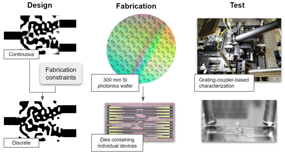
In this work, we report the first successful demonstration of inverse-designed photonics in a commercial silicon photonics process. The designs were fabricated as part of the AIM Photonics 300 mm wafer multi-project wafer (MPW) foundry offering 23. We demonstrate four different devices fabricated using a single fully-etched layer of thick silicon, surrounded on all sides by silicon dioxide cladding. These devices are compact, with footprints of only several micrometers across, and have comparable performance and reproducibility to previous inverse-designed devices fabricated using electron-beam lithography (Fig. 1).
Results
Design
The goal of inverse design is to automate the design process. First, a human designer broadly specifies the desired performance and other characteristics of the device, such as the desired transmission through an output port with a given design area 18, 19, 24. An optimization algorithm is then used to search the space of available designs using gradient-based optimization, which can efficiently optimize over tens or even hundreds of thousands of design degrees of freedom. By using adjoint sensitivity analysis, the gradient can be efficiently computed using one additional electromagnetic simulation, regardless of the number of design parameters 12, 24, 25, 26.
To successfully fabricate devices at a foundry, the designs should be robustly resolved using photolithography. In principle, it would be possible to directly incorporate a lithography model into the optimization algorithm, but this requires detailed knowledge of the lithography parameters used by the foundry. In lieu of directly incorporating a lithography model, 18 proposed using two constraints as heuristics: a minimum gap and a minimum radius of curvature. More specifically, a minimum radius of curvature constraint is applied to all material interfaces, preventing the formation of any sharp cusps and corners. A minimum gap constraint prevents the formation of narrow gaps and bridges. To ensure robustness to fabrication errors, all devices were designed to operate over as broad of a range of wavelengths as possible, which has previously been shown to be an effective heuristic for fabrication robustness. As will be demonstrated through the experimental measurements, these two fabrication constraints, along with broadband optimization, are sufficient for creating devices that can be reliably fabricated at commercial foundries.
Spatial mode multiplexer
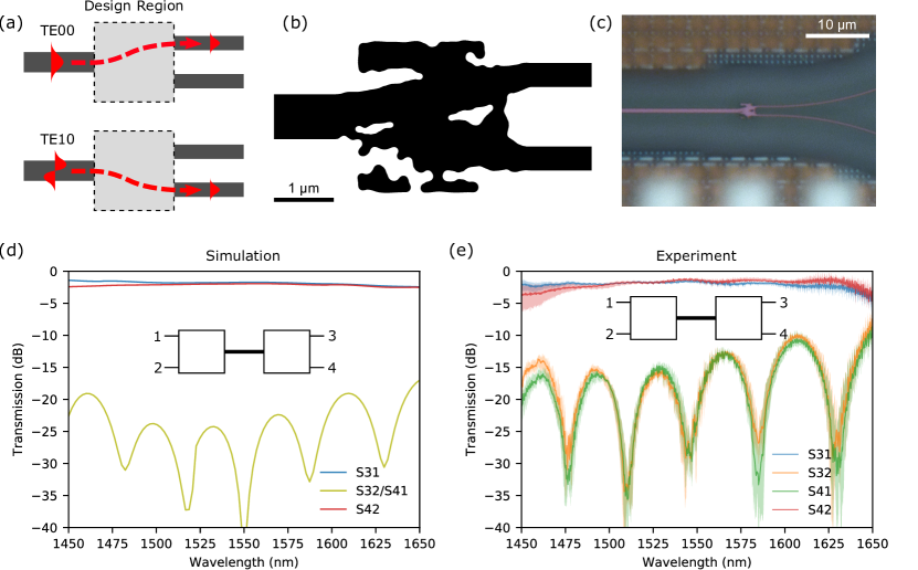
First we consider a compact spatial mode multiplexer, which separates the fundamental and second-order modes of a wide multi-mode input waveguide, and routes them to separate wide single-mode output waveguides (Fig. 2(a)). The device was designed by first allowing the permittivity in the design region to continuously vary between that of silicon and silicon dioxide, before applying thresholding and switching to boundary optimization 18. During boundary optimization, a 70 nm minimum radius of curvature and 90 nm minimum gap constraint were applied. This resulted in a design with a complex and non-intuitive topology and a compact footprint of (Fig. 2(b, c)).
To test the spatial mode multiplexer, two multiplexers were placed back-to-back, joined by an segment of multi-mode waveguide. This allowed the device to be measured using standard single-mode optical fibers and grating couplers. Fig. 2(d) and (e) show that the simulated and measured S-parameters agree well with each other. In addition, the fabricated devices are very reproducible: the S-parameters of the three instances from three dies are closely aligned. Extracting the S-parameters of a single device is straightforward (Methods): over the entire operating bandwidth of , the insertion loss is , and the crosstalk suppression is .
Wavelength demultiplexer
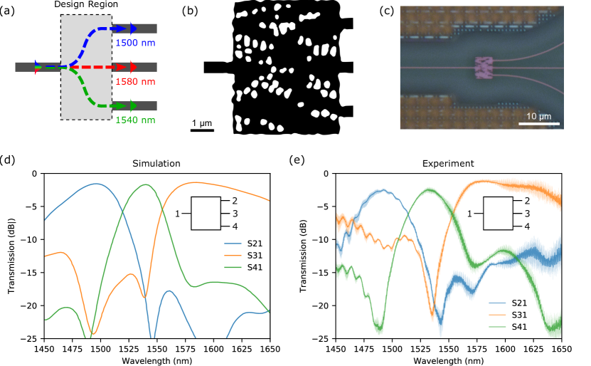
Next we consider a 3-channel wavelength demultiplexer, designed to separate , , and light (Fig. 3(a)). We used “neighbour biasing” in the continuous stage of optimization to produce a good starting point for boundary optimization 19. The minimum radius of curvature was , and the minimum gap width was . The design (Fig. 3(b, c)) is highly non-intuitive but compact, with a footprint of only .
The simulated and measured S-parameters are presented in Fig. 3(d) and (e). The measured spectra exhibit three clear passbands, showing that the device functions as intended, although the crosstalk is somewhat higher. The reproducibility is also excellent: the three fabricated instances have nearly identical transmission. The insertion loss for the 3 output channels are at , at , and at . The crosstalk suppression are and , respectively.
Directional coupler
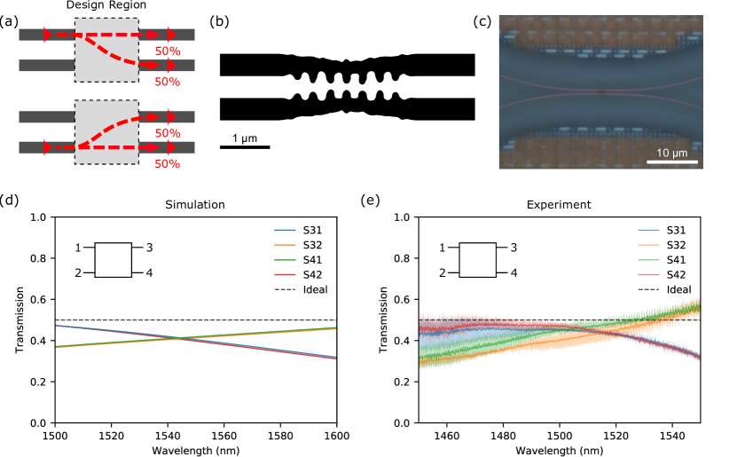
The third design is a 50-50 directional coupler that takes light from either of its two input waveguides and equally divides it between the two output waveguides (Fig. 4(a)). The same two-stage design process was used as for the spatial mode multiplexer, with minimum radius of curvature of and minimum gap of . With a footprint of , the final design is significantly more compact than most designs in the literature (Fig. 4(b)). Interestingly, the structure strongly resembles a conventional grating-assisted directional coupler, despite the complete lack of human intervention throughout the design process.
The design is relatively broadband, with reasonably matched output powers over a bandwidth in both simulation (Fig. 4(d)) and measurement (Fig. 4(e)). Over a bandwidth, the fabricated couplers have an average insertion loss of and power imbalance. There is, however, a significant wavelength shift between the simulated and measured devices, likely due to fabrication errors: the design has a central wavelength of , whereas the measured devices operate around .
Power splitter
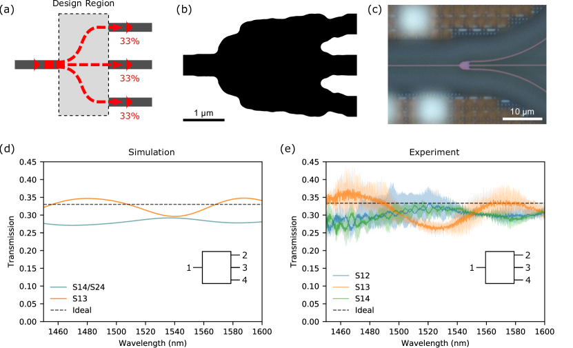
The last design is a broadband three-way power splitter that equally splits the power from an input waveguide into three output waveguides (Fig. 5(a)). In contrast to the previous designs, the power splitter was designed using only boundary optimization with minimum radius of curvature of , yielding a design (Fig. 5(b)) that resembles a compact multi-mode interferometer (MMI) coupler 18. The final design has a footprint of .
The simulated and measured S-parameters for the three-way power splitter are given in Fig. 5(d) and (e). The splitting is very broadband, operating nominally from to . The simulated and measured S-parameters match quite closely, although there is a shift in the transmission fringes. The design was constrained to have reflection symmetry across the horizontal axis, resulting in and parameters that are identical in simulation and nearly identical in measurement. Over the full operating bandwidth, the splitter has an insertion loss of , and a power imbalance of .
Discussions
All four designs appear to be quite robust to fabrication errors. The device-to-device variability across the three dies, each containing a single instance of all designs, was approximately equal to our measurement uncertainty of , limited mostly by grating coupler variability. This consistency suggests that they are robust to typical fabrication errors, such as defocusing in photolithography or variation in layer thicknesses. Furthermore, both the wavelength demultiplexer 19 and 3-way power splitter 18 were previously fabricated using electron-beam lithography and had comparable performance to the present devices. This implies that high-resolution electron-beam lithography is not necessary for fabricating these complex designs; industry-standard photolithography is sufficient, so long as the designs are properly constrained.
In summary, we have experimentally demonstrated a photonic inverse design process that is compatible with industry-standard photonics foundries. By incorporating fabrication constraints we have eliminated small features that cannot be resolved using photolithography. A wide breadth of devices were demonstrated, illustrating the flexibility of the method. These results show that inverse design is a suitable method for designing practical integrated photonic devices and has the potential to revolutionize the field by enabling a new generation of exceedingly compact and high performance devices.
Methods
Design algorithms
All devices were designed using our adjoint optimization based implementation of photonic inverse design 18, 19, 24. Our inverse design algorithm proceeds in two stages. In the first stage, the permittivity is allowed to continuously vary between those of the available materials (e.g. silicon and silicon dioxide) at every point in the design. The design is then thresholded to produce a binary structure consisting of only two materials, which is used as the starting condition for the next stage. In the second stage, only the material boundaries are optimized by using a level set representation of the structure 27. Under the level set representation, the boundary of the device is defined as the zero crossing of a continuous function 18. The implicit nature of the level set representation makes it trivial to handle changes in topology, such as the merging or splitting of holes, and does not require one to perform complex additional steps such as re-meshing.
The computational cost of inverse design is dominated by the required electromagnetic simulations, which were performed using Maxwell FDFD 28, 29, a GPU-based implementation of the finite-difference frequency-domain (FDFD) method, with a spatial step size of . The Maxwell FDFD simulation software is available on GitHub at https://github.com/stanfordnqp/maxwell-b under the GNU General Public License v3.0. Final broadband verification simulations were then performed using commercial Lumerical FDTD (finite-difference time-domain) software 30. All simulations and design were performed on a server with an Intel Core i7-5820K processor, 64GB of RAM, and three Nvidia Titan Z graphics cards.
The spatial mode multiplexer, 3-way power splitter, and 50-50 directional coupler were optimized over 6 equally spaced wavelengths from to 18. This resulted in designs which operated well over a broad wavelength range. Meanwhile, the wavelength demultiplexer was optimized at the three channel wavelengths of , , and 19.
Fabrication
As discussed in the main text, the designs were fabricated on an AIM Photonics 300 mm wafer multi-project wafer (MPW) run 23. We waived the minimum width DRC (design-rule check) rule for the spatial mode multiplexer, 50-50 directional coupler, and wavelength demultiplexer, and waived the minimum separation rule for the spatial mode multiplexer and wavelength demultiplexer. However, the designs were all successfully resolved by the immersion lithography used in the AIM Photonics process, which can produce features as small as across 31.
Measurement
We measured the transmission through the devices by a home-built grating-coupling setup. The input and output fibers were mounted on flexture stages with piezo nanopositioners (Thorlabs NanoMax) and were 10 degrees from normal to the chip plane. We used a bandpass filtered supercontinuum laser (Fianium WhiteLase SC-400-4) as light source and an optical spectrum analyzer (Agilent 86140B) to measure the transmitted power spectra. The fibers were automatically aligned to maximize the transmitted power before each measurement. The power spectra of individual devices are reproducible to 0.5 dB. We obtain the transmission spectra of the devices by normalizing against the two straight waveguides on each chip. The transmission of these two straight waveguides have a variation of up to on all three chips and we use the average spectra to normalize. In the figures containing experimental transmission data, the solid lines are the average spectra and the shaded regions the span of values from all three chips.
Extracting S-parameters for spatial mode demultiplexer
Extracting the S-parameters for a single multiplexer from the measured data is relatively straightforward. The and parameters of the back-to-back structure are a measure of insertion loss, and are equal to double the insertion loss of a single multiplexer. Meanwhile, the and parameters are measures of the crosstalk. In this test structure, there are two dominant crosstalk paths: light can be coupled into the wrong mode of the multi-mode waveguide by the first multiplexer, and light can be coupled into the wrong output waveguide by the second multiplexer. Since the and modes of the multi-mode waveguide have different propagation constants, this results in a fringing pattern in the and spectra.
Acknowledgements
This work was supported by AIM Photonics, and sponsored by the Air Force Research Laboratory via agreement number FA8650-15-2-5220, the Air Force Office of Scientific Research MURI on Attojoule Optoelectronics via award number FA9550-17-1-0002, and the Gordon and Betty Moore Foundation via grant GBMF4744.
References
- Mounie and Malinge 2019 Mounie, E.; Malinge, J.-L. Silicon Photonics and Photonic Integrated Circuits; 2019
- Rahim et al. 2018 Rahim, A.; Spuesens, T.; Baets, R.; Bogaerts, W. Open-Access Silicon Photonics: Current Status and Emerging Initiatives. Proc. IEEE 2018, 106, 2313–2330
- Sun et al. 2013 Sun, J.; Timurdogan, E.; Yaacobi, A.; Hosseini, E. S.; R.Watts, M. Large-scale nanophotonic phased array. Nature 2013, 493, 195 – 199
- Miller et al. 2018 Miller, S. A.; Phare, C. T.; Chang, Y.; Ji, X.; Gordillo, O. A. J.; Mohanty, A.; Roberts, S. P.; Shin, M. C.; Stern, B.; Zadka, M.; Lipson, M. 512-Element Actively Steered Silicon Phased Array for Low-Power LIDAR. 2018 Conference on Lasers and Electro-Optics (CLEO). 2018; pp 1–2
- Shen et al. 2017 Shen, Y.; Harris, N. C.; Skirlo, S.; Prabhu, M.; Baehr-Jones, T.; Hochberg, M.; Sun, X.; Zhao, S.; Larochelle, H.; Englund, D.; Soljačić, M. Deep learning with coherent nanophotonic circuits. Nature Photonics 2017, 11, 441
- Komljenovic et al. 2016 Komljenovic, T.; Davenport, M.; Hulme, J.; Liu, A. Y.; Santis, C. T.; Spott, A.; Srinivasan, S.; Stanton, E. J.; Zhang, C.; Bowers, J. E. Heterogeneous silicon photonic integrated circuits. Journal of Lightwave Technology 2016, 34, 20–35
- Reed 2008 Reed, G. T. Silicon Photonics: The State of the Art; John Wiley & Sons: Chichester, West Sussex, U.K., 2008
- Mutapcica et al. 2009 Mutapcica, A.; Boyd, S.; Farjadpour, A.; Johnson, S. G.; Avnielb, Y. Robust design of slow-light tapers in periodic waveguides. Eng. Optimiz. 2009, 41, 365 – 384
- Jensen and Sigmund 2011 Jensen, J. S.; Sigmund, O. Topology optimization for nano-photonics. Laser Photonics Rev. 2011, 5, 308 – 321
- Lalau-Keraly et al. 2013 Lalau-Keraly, C. M.; Bhargava, S.; Miller, O. D.; Yablonovitch, E. Adjoint shape optimization applied to electromagnetic design. Opt. Express 2013, 21, 21693 – 21701
- Lu and Vučković 2013 Lu, J.; Vučković, J. Nanophotonic computational design. Opt. Express 2013, 21, 13351 – 13367
- Niederberger et al. 2014 Niederberger, A. C. R.; Fattal, D. A.; Gauger, N. R.; Fan, S.; Beausoleil, R. G. Sensitivity analysis and optimization of sub-wavelength optical gratings using adjoints. Opt. Express 2014, 22, 12971 – 12981
- Piggott et al. 2015 Piggott, A. Y.; Lu, J.; Lagoudakis, K. G.; Petykiewicz, J.; Babinec, T. M.; Vučković, J. Inverse design and demonstration of a compact and broadband on-chip wavelength demultiplexer. Nature Photonics 2015, 9, 374–377
- Frellsen et al. 2016 Frellsen, L. F.; Ding, Y.; Sigmund, O.; Frandsen, L. H. Topology optimized mode multiplexing in silicon-on-insulator photonic wire waveguides. Opt. Express 2016, 24, 16866 – 16873
- Sell et al. 2017 Sell, D.; Yang, J.; Doshay, S.; Yang, R.; Fan, J. A. Large-angle, multifunctional metagratings based on freeform multimode geometries. Nano letters 2017, 17, 3752–3757
- Michaels and Yablonovitch 2018 Michaels, A.; Yablonovitch, E. Inverse design of near unity efficiency perfectly vertical grating couplers. Opt. Express 2018, 26, 4766–4779
- Molesky et al. 2018 Molesky, S.; Lin, Z.; Piggott, A. Y.; Jin, W.; Vucković, J.; Rodriguez, A. W. Inverse design in nanophotonics. Nature Photonics 2018, 12, 659
- Piggott et al. 2017 Piggott, A. Y.; Petykiewicz, J.; Su, L.; Vučković, J. Fabrication-constrained nanophotonic inverse design. Sci. Rep. 2017, 7, 1786
- Su et al. 2018 Su, L.; Piggott, A. Y.; Sapra, N. V.; Petykiewicz, J.; Vučković, J. Inverse Design and Demonstration of a Compact on-Chip Narrowband Three-Channel Wavelength Demultiplexer. ACS Photonics 2018, 5, 301–305
- Dory et al. 2019 Dory, C.; Vercruysse, D.; Yang, K. Y.; Sapra, N. V.; Rugar, A. E.; Sun, S.; Lukin, D. M.; Piggott, A. Y.; Zhang, J. L.; Radulaski, M.; Lagoudakis, K. G.; Su, L.; Vučković, J. Inverse-designed diamond photonics. Nature Communications 2019, 10, 3309
- Hoffman et al. 2019 Hoffman, G. B.; Dallo, C.; Starbuck, A.; Hood, D.; Pomerene, A.; Trotter, D.; DeRose, C. T. Improved broadband performance of an adjoint shape optimized waveguide crossing using a Levenberg-Marquardt update. Optics Express 2019, 27, 24765–24780
- Mak et al. 2016 Mak, J. C.; Sideris, C.; Jeong, J.; Hajimiri, A.; Poon, J. K. Binary particle swarm optimized 2 2 power splitters in a standard foundry silicon photonic platform. Optics letters 2016, 41, 3868–3871
- Fahrenkopf et al. 2019 Fahrenkopf, N. M.; McDonough, C.; Leake, G. L.; Su, Z.; Timurdogan, E.; Coolbaugh, D. D. The AIM Photonics MPW: A Highly Accessible Cutting Edge Technology for Rapid Prototyping of Photonic Integrated Circuits. IEEE Journal of Selected Topics in Quantum Electronics 2019, 25, 1–6
- Piggott 2018 Piggott, A. Y. Automated design of photonic devices. Ph.D. thesis, Stanford University, 2018
- Giles and Pierce 2000 Giles, M. B.; Pierce, N. A. An Introduction to the Adjoint Approach to Design. Flow, Turbulence and Combustion 2000, 65, 393–415
- Johnson 2012 Johnson, S. G. Notes on Adjoint Methods for 18.335. 2012; http://math.mit.edu/~stevenj/18.336/adjoint.pdf
- Osher and Fedkiw 2003 Osher, S.; Fedkiw, R. Level Set Methods and Dynamic Implicit Surfaces; Springer: New York, U.S.A., 2003
- Shin and Fan 2012 Shin, W.; Fan, S. Choice of the perfectly matched layer boundary condition for frequency-domain Maxwell’s equations solvers. J. Comput. Phys. 2012, 231, 3406 – 3431
- Shin and Fan 2013 Shin, W.; Fan, S. Accelerated solution of the frequency-domain Maxwell’s equations by engineering the eigenvalue distribution. Opt. Express 2013, 21, 22578 – 22595
- 30 Lumerical Inc., FDTD: 3D Electromagnetic Simulator. https://www.lumerical.com/products/
- Totzeck et al. 2007 Totzeck, M.; Ulrich, W.; Göhnermeier, A.; Kaiser, W. Pushing deep ultraviolet lithography to its limits. Nature Photonics 2007, 1, 629