Enhanced Electronic Transport in Disordered Hyperuniform Two-Dimensional Amorphous Silica
Abstract
Disordered hyperuniformity (DHU) is a recently proposed new state of matter, which has been observed in a variety of classical and quantum many-body systems. DHU systems are characterized by vanishing infinite-wavelength density fluctuations and are endowed with unique novel physical properties. Here we report the first discovery of disordered hyperuniformity in atomic-scale 2D materials, i.e., amorphous silica composed of a single layer of atoms, based on spectral-density analysis of high-resolution transmission electron microscope images. Subsequent simulations suggest that the observed DHU is closely related to the strong topological and geometrical constraints induced by the local chemical order in the system. Moreover, we show via large-scale density functional theory calculations that DHU leads to almost complete closure of the electronic band gap compared to the crystalline counterpart, making the material effectively a metal. This is in contrast to the conventional wisdom that disorder generally diminishes electronic transport and is due to the unique electron wave localization induced by the topological defects in the DHU state.
Disorder hyperuniform (DHU) systems are a unique class of disordered systems which suppress large-scale density fluctuations like crystals and yet possess no Bragg peaks Torquato and Stillinger (2003); Zachary and Torquato (2009). For a point configuration (e.g., a collection of particle centers of a many-body system), hyperuniformity is manifested as the vanishing structure factor in the infinite-wavelength (or zero-wavenumber) limit, i.e., , where is the wavenumber. In this case of a random field, the hyperuniform condition is given by , where is the spectral density Zachary and Torquato (2009). It has been suggested that hyperuniformity can be considered as a new state of matter Torquato and Stillinger (2003), which possesses a hidden order in between of that of a perfect crystal and a totally disordered system (e.g. a Poisson distribution of points).
Recently, a wide spectrum of physical and biological systems have been identified to possess the remarkable property of hyperuniformity, which include the density fluctuations in early universe Gabrielli et al. (2002), disordered jammed packing of hard particles Donev et al. (2005); Zachary et al. (2011); Jiao and Torquato (2011); Chen et al. (2014), certain exotic classical ground states of many-particle systems Zachary and Torquato (2011); Torquato et al. (2015); Uche et al. (2004); Batten et al. (2008, 2009); Lebowitz (1983); Zhang et al. (2015a, b), jammed colloidal systems Berthier et al. (2011); Kurita and Weeks (2011); Hunter and Weeks (2012); Dreyfus et al. (2015), driven non-equilibrium systems Hexner and Levine (2015); Jack et al. (2015); Weijs et al. (2015); Tjhung and Berthier (2015), certain quantum ground states Torquato et al. (2008); Feynman and Cohen (1956), avian photoreceptor patterns Jiao et al. (2014), organization of adapted immune systems Mayer et al. (2015), amorphous silicon Hejna et al. (2013); Xie et al. (2013), a wide class of disordered cellular materials Klatt et al. (2019), dynamic random organizating systems Hexner and Levine (2017); Hexner et al. (2017); Weijs and Bartolo (2017); Lei et al. (2019); Lei and Ni (2019), and even the distribution of primes on the number axis Torquato et al. (2019). In addition, it has been shown that hyperuniform materials can be designed to possess superior physical properties including large isotropic photonic band gaps Florescu et al. (2009); Man et al. (2013a, b), optimized transport properties Zhang et al. (2016), mechanical properties Xu et al. (2017) as well as optimal multi-functionalities Torquato and Chen (2018). Designer DHU materials have also been successfully fabricated or synthesized using different techniques Haberko et al. (2013); Zito et al. (2015).
In this letter, we report the discovery of hyperuniformity in amorphous 2D silica (conventionally modeled as “continuous random networks” Binder and Kob (2011)), based on the analysis of aberration corrected transmission electron microscopy (TEM) images of the material. To the best of our knowledge, this is the first discovery of disordered hyperuniformity in atomic scale 2D materials (i.e., those composed of a single layer of atoms), which can possess unique novel electronic, magnetic and optical properties compared to their bulk counterparts.
We show via simulations that the observed DHU in amorphous silica is closely related to the strong topological and geometrical constraints induced by the local chemical order in the system. In addition, our density functional theory calculations show that DHU significantly reduces the electronic band gap in 2D amorphous silica, leading to almost complete closure of the band gap compared to the crystalline counterpart. This is in contrast to the conventional wisdom that disorder generally diminishes electronic transport and is due to the unique electron wave localization induced by DHU.
Hyperuniformity in 2D amorphous silica. We first analyze the high-resolution transmission electron microscopy (TEM) images of 2D amorphous silica, see Fig.1a. The materials samples were fabricated using chemical vapor deposition (CVD) and the procedure for obtaining the imaging data set was reported in detail in Ref. Huang et al. (2013) and briefly described in the Supporting Information (SI). As shown in Fig. 1a, the black spots (with diffusive boundaries) represent the silicon atoms. The micrographs are processed to retain the distribution information of the silicon atoms by thresholding and fitting the grayness intensity distribution associated with each silicon atom using a Gaussian function, i.e., , where is the maximal intensity, is the center of the silicon atom and is an effective radius.
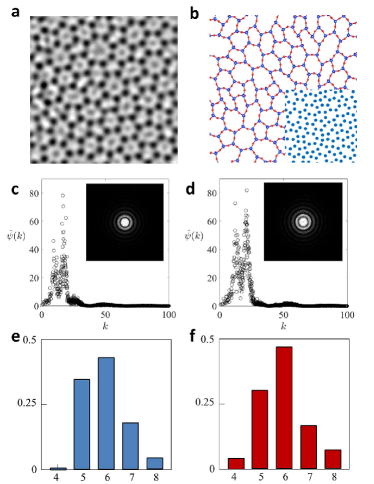
The associated spectral density (where is the wave-vector) is computed following Ref. Ma and Torquato (2017) and shown in the inset of Fig.1c. The angularly averaged (with ) is shown Fig.1c. We note that the spectral density analysis (instead of structure factor) is employed here to efficiently utilize all of the information on Si atom distributions contained in the TEM micrographs and minimize the possible systematic errors induced by converting the intensity map into center distributions. It can be seen that is fully isotropic and the scattering is completely suppressed at infinite wavelength, i.e., with for small values, which indicates that the 2D amorphous silica samples analyzed are hyperuniform (see SI for detailed scaling analysis).
Next, we computationally generate disordered hyperuniform silica networks. We note that unlike 3D amorphous materials such as metallic glasses which can be simulated by numerically quenching a high temperature liquid state, even very rapid quenching of a 2D materials will lead to a highly crystalline materials with a small number of local defects. Such defected crystalline materials clearly cannot represent the experimentally obtained DHU amorphous silicon. Together with the observation that the 2D silica systems are HU, this motivates us to employ a structure-based method, which is a two-step approach.
In the first step, a three-coordinated DHU network is generated using a modified “collective coordinate” approach Batten et al. (2008), in which a random initial configuration of points is gradually evolved to match a prescribed targeted structure factor while simultaneously satisfying mutual exclusion volume constraints. The targeted for drives the system to a hyperuniform state and the exclusion volume constraints ensure the final configuration can be feasibly mapped to an amorphous silica network. In the second step, the obtained point configuration is mapped to a three-coordinated network by connecting a point with its three nearest neighbors. This network is further converted to a silica network, by placing a silicon atom centered at each point and placing an oxygen atom at the mid-point of the two connected silicon atoms. We then perform molecular statics simulations using the Si-O potential based on the Tersoff parameterization Munetoh et al. (2007) as implemented in the LAMMPS program Plimpton (1995) to optimize the constructed silica network to physically metastable states by minimizing their total potential energy.
The spectral density of the simulated amorphous silica network (see Fig.1b) is computed by placing a Gaussian kernel function at the center of each silicon atom and is shown in Fig.1d. It can be clearly seen that of the simulated network agrees very well with the experimental data for all wave numbers including the zero- limit, i.e., with for small values (see SI for detailed scaling analysis and comparison to experimental results).
We note that in the second step of the simulation (i.e., the potential energy minimization), hyperuniformity (i.e., the small values of ) is not constrained anymore. The evolution of the system is dominated by the interactions of atoms and constrained by the topology, and the positions of the atoms have been significantly perturbed compared to the final configuration obtained in the first step. Yet the resulting system is still hyperuniform. This result suggests the strong geometrical and topological constraints, i.e., the bond length and angle associated with the Si-O bonds as well as 3-coordinated configurations, induced by the local chemical order could lead to the observed hyperuniformity in the system.
We also obtain and compare the number of -fold rings (where ) formed by silicon atoms in both the experimental and simulated networks, see Fig.1(e) and 1(f). The ring statistics for the two systems again agree very well with one another. In addition, the comparison of local structural statistics of the experimental and numerical systems, including the pair correlation function and nearest neighbor distribution of the Si atoms also show excellent agreement (see SI for details). These results indicate our numerical network model can provide a statistically accurate structural representation of the 2D amorphous silica system by capturing key correlations on both large and small length scales as well as the local topological order. Therefore, we expect that the physical properties computed based on the numerical network model should also be representative of those of the experimental system.
What is the origin of DHU in 2D amorphous silica? We note that as a first approximation, the 2D silica glass can be considered as obtained from a 2D crystalline silica network by continuously introducing the Stone-Wales (SW) defects Stone and Wales (1986), which change the topology of the network. However, the SW defects do not affect the number of particles within a large observation window, since the SW transformation is localized and only affects a pair of atoms on the single-bond scale. Nonetheless, SW transformations of atom pairs on the boundary of the observation window might lead to a bounded fluctuation of particle numbers, which are scaled with the surface area of the window. Therefore, the SW defects should preserve hyperuniformity in the system. We provide numerical evidence for this speculation in the SI. Although the actual 2D amorphous silica possesses a structure that deviates from the ideal SW transferred crystalline network, the above argument could provide a possible explanation of the observed DHU in the system.
Disordered hyperuniformity significantly reduces electronic band gap. We use the simulated DHU SiO2 networks to calculate its density of states (DOS) at the DFT-PBE Perdew et al. (1996) level of theory. Specifically, the DHU structure consists of three sublayers (1800 atoms; 600 Si atoms and 1200 O atoms). For comparison, we also create a supercell of 2D crystalline SiO2 with the same number of Si and O atoms. Several models of 2D crystalline SiO2 have been studied using DFT calculations in the literature Gao et al. (2017). Here we refer 2D crystalline SiO2 to the hexagonal bilayer crystalline network observed in experiment Huang et al. (2012).
We use numerical atomic orbitals Chen et al. (2010) as implemented in the ABACUS package Li et al. (2016) for calculating the electronic structure. The simulation methods and parameters can be found in Ref. ref . For comparison, we also compute the DOS for 2D hexagonal crystalline SiO2. The energy difference between the 2D DHU and hexagonal crystalline SiO2 calculated from the Tersoff potential and DFT are both positive and comparable (0.074 and 0.134 eV/atom, respectively). The positive energy differences indicate that the crystalline structure is more energetically stable than the DHU structure. Nevertheless, the TEM image (see Fig.1(a)) shows that the experimental atomic structure of 2D amorphous SiO2 is drastically different from the crystalline model. By contrast, the high similarity between the DHU model and experimentally observed atomic structure reveals the metastable nature of DHU systems.
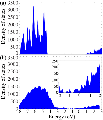
Figure 2 (a) shows that the 2D crystalline SiO2 is essentially an insulator with a predicted band gap of 5.31 eV, consistent with the previously reported band gap of 5.48 eV calculated for a unit cell at the same level of theory Gao et al. (2016). By contrast, we observe from Fig. 2(b) that a small but finite number of states occupy the Fermi level of the DHU structure, showing metallic behavior of the electrons with a typical band gap of meV. This is comparable to the thermal fluctuations at room temperature meV. In other words, the disordered hyperuniformity fundamentally changes the electrical transport behavior of 2D SiO2, from an effective insulator at room temperature (as in the crystalline form) to an effective metal (as in the DHU form).
From Fig. 2(b), we estimate the density of the electrons that contribute to the electrical conductivity of the DHU structure at room temperature. By integrating the number of states in the energies ranging from 25 meV (corresponding to the thermal energy) to the Fermi level in Fig. 2(b), we determine as 2.33 1012 cm-2. This magnitude belongs to the category of “high doping” (e.g., 6.0 and 9.2 cm-2) applied to common 2D semiconductors such as WS2 and MoS2 Yang et al. (2014). To put it another way, considering the electron density alone, the conductivity associated with the DHU structure could be comparable to those of the 2D materials.
To better understand this metallic behavior of DHU 2D SiO2, we compute the charge densities within an energy window of 0.5 eV below the highest occupied molecular orbital (HOMO) level for the crystalline structure and below the Fermi level for the DHU structure. For the former structure, Fig.3(a) (a complete version of Fig.3 can be found in the supplemental material) shows that the electrons are distributed around Si and O atoms in the entire structure, i.e., fully occupying the valence bands. The amount of these electrons is significant, as can be seen from the large DOS below the HOMO level. But these electrons cannot be thermally excited at room temperature to the conduction bands due to the large band gap, leading to zero electrical conductivity for pure 2D crystalline SiO2.
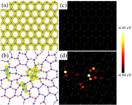
On the other hand, for the DHU structure, the number of valence electrons in the same energy window is much less, resulting in a low carrier density but nevertheless, a non-zero conductivity. A closer look at the slightly wider energy window associated with lowest density of states (e.g., -20 eV) reveals that the distribution of states still forms an almost continuous spectrum of peaks, see the inset in Fig. 2(b). Figure 3(b) reveals that the valence electrons contributing to the conductivity originate from a small portion of the Si and O atoms in the DHU system.
Topological defects in DHU SiO2 lead to electron localization with high energies. To understand why the electrons are localized around these atoms, we show in Fig. 3(c) and 3(d) the distributions of the computed potential energies using the Tersoff potential for the crystalline and DHU systems, respectively. Consistent with Fig. 3(a), Fig. 3(c) shows that the potential energies are homogeneously distributed in the crystalline system. On the contrary, for the DHU system, we observe from Fig. 3(d) that the potential energies possess a highly heterogeneous distribution, with significantly higher energies localized in regions where the atomic arrangements significantly deviates from the 6-fold hexagonal configuration. These are topological defects which are necessary to achieve DHU in amorphous 2D silica. Importantly, the high-energy localizations perfectly coincide with the electron localizations (see Figure 3(b)), indicating that the local potential energies due to the topological defects induced by DHU are sufficiently high to activate the electrons to the energy levels near the Fermi energy.
Electron localization in a disordered system is generally associated with a number of exotic physical phenomena Kramer and MacKinnon (1993) such as metal-to-insulator transitions suggested by Anderson Anderson (1958). The electron localization in the DHU silica system appears to be phenomenologically different from the Anderson localization, as the DHU localization gives rise the opposite (i.e., insulator-to-metal) transition. A mathematical model based on model Hamiltonian that considers the disordered potential needs to be devised in order to investigate the electrical transport property of the localized electrons. Furthermore, whether the insulator-to-metal transition also occurs in other 2D DHU semiconductors/insulators remains unknown and is certainly worth exploring.
In summary, we have discovered, for the first time, disordered hyperuniformity in 2D amorphous materials, and showed that DHU fundamentally changes the electronic transport behaviors in the material, making 2D DHU silica metallic. This interesting prediction clearly awaits for experimental confirmation. We also showed that the metallic behavior (i.e., with a virtually continuous spectrum of DOS without significant band gaps in DHU silica) is resulted from the localization of high-energy states due to the topological defects induced by DHU. Since the observed DHU in 2D silica is associated with the local topological and geometrical constraints common in many 2D materials, we would expect to observe DHU and thus, the metallic behavior, in the amorphous states of other 2D materials, should such states be metastable at least. With the increasing interest in 2D amorphous materials, we expect our methods of building realistic structural model of amorphous 2D material systems along with large-scale DFT calculations to be applicable to a wide range of other 2D materials such as graphene Van Tuan et al. (2012) and molybdenum disulfide Zhang et al. (2015c) in the amorphous form.
Acknowledgments We thank P. Y. Huang for helpful discussion and sharing TEM images of amorphous silica. Y. Z. and H. N. thank Arizona State University (ASU) for the University Graduate Fellowship. L. L. and H.Z. thank the start-up funds from ASU. The DFT calculations have been done on the USTC HPC facilities.
References
- Torquato and Stillinger (2003) S. Torquato and F. H. Stillinger, Physical Review E 68, 041113 (2003).
- Zachary and Torquato (2009) C. E. Zachary and S. Torquato, Journal of Statistical Mechanics: Theory and Experiment 2009, P12015 (2009).
- Gabrielli et al. (2002) A. Gabrielli, M. Joyce, and F. S. Labini, Physical Review D 65, 083523 (2002).
- Donev et al. (2005) A. Donev, F. H. Stillinger, and S. Torquato, Physical review letters 95, 090604 (2005).
- Zachary et al. (2011) C. E. Zachary, Y. Jiao, and S. Torquato, Physical review letters 106, 178001 (2011).
- Jiao and Torquato (2011) Y. Jiao and S. Torquato, Physical Review E 84, 041309 (2011).
- Chen et al. (2014) D. Chen, Y. Jiao, and S. Torquato, The Journal of Physical Chemistry B 118, 7981 (2014).
- Zachary and Torquato (2011) C. E. Zachary and S. Torquato, Physical Review E 83, 051133 (2011).
- Torquato et al. (2015) S. Torquato, G. Zhang, and F. Stillinger, Physical Review X 5, 021020 (2015).
- Uche et al. (2004) O. U. Uche, F. H. Stillinger, and S. Torquato, Physical Review E 70, 046122 (2004).
- Batten et al. (2008) R. D. Batten, F. H. Stillinger, and S. Torquato, Journal of Applied Physics 104, 033504 (2008).
- Batten et al. (2009) R. D. Batten, F. H. Stillinger, and S. Torquato, Physical review letters 103, 050602 (2009).
- Lebowitz (1983) J. L. Lebowitz, Physical Review A 27, 1491 (1983).
- Zhang et al. (2015a) G. Zhang, F. H. Stillinger, and S. Torquato, Physical Review E 92, 022119 (2015a).
- Zhang et al. (2015b) G. Zhang, F. H. Stillinger, and S. Torquato, Physical Review E 92, 022120 (2015b).
- Berthier et al. (2011) L. Berthier, P. Chaudhuri, C. Coulais, O. Dauchot, and P. Sollich, Physical review letters 106, 120601 (2011).
- Kurita and Weeks (2011) R. Kurita and E. R. Weeks, Physical Review E 84, 030401 (2011).
- Hunter and Weeks (2012) G. L. Hunter and E. R. Weeks, Reports on progress in physics 75, 066501 (2012).
- Dreyfus et al. (2015) R. Dreyfus, Y. Xu, T. Still, L. A. Hough, A. Yodh, and S. Torquato, Physical Review E 91, 012302 (2015).
- Hexner and Levine (2015) D. Hexner and D. Levine, Physical review letters 114, 110602 (2015).
- Jack et al. (2015) R. L. Jack, I. R. Thompson, and P. Sollich, Physical review letters 114, 060601 (2015).
- Weijs et al. (2015) J. H. Weijs, R. Jeanneret, R. Dreyfus, and D. Bartolo, Physical review letters 115, 108301 (2015).
- Tjhung and Berthier (2015) E. Tjhung and L. Berthier, Physical review letters 114, 148301 (2015).
- Torquato et al. (2008) S. Torquato, A. Scardicchio, and C. E. Zachary, Journal of Statistical Mechanics: Theory and Experiment 2008, P11019 (2008).
- Feynman and Cohen (1956) R. Feynman and M. Cohen, Physical Review 102, 1189 (1956).
- Jiao et al. (2014) Y. Jiao, T. Lau, H. Hatzikirou, M. Meyer-Hermann, J. C. Corbo, and S. Torquato, Physical Review E 89, 022721 (2014).
- Mayer et al. (2015) A. Mayer, V. Balasubramanian, T. Mora, and A. M. Walczak, Proceedings of the National Academy of Sciences 112, 5950 (2015).
- Hejna et al. (2013) M. Hejna, P. J. Steinhardt, and S. Torquato, Physical Review B 87, 245204 (2013).
- Xie et al. (2013) R. Xie, G. G. Long, S. J. Weigand, S. C. Moss, T. Carvalho, S. Roorda, M. Hejna, S. Torquato, and P. J. Steinhardt, Proceedings of the National Academy of Sciences 110, 13250 (2013).
- Klatt et al. (2019) M. A. Klatt, J. Lovrić, D. Chen, S. C. Kapfer, F. M. Schaller, P. W. Schönhöfer, B. S. Gardiner, A.-S. Smith, G. E. Schröder-Turk, and S. Torquato, Nature communications 10, 811 (2019).
- Hexner and Levine (2017) D. Hexner and D. Levine, Physical review letters 118, 020601 (2017).
- Hexner et al. (2017) D. Hexner, P. M. Chaikin, and D. Levine, Proceedings of the National Academy of Sciences 114, 4294 (2017).
- Weijs and Bartolo (2017) J. H. Weijs and D. Bartolo, Physical review letters 119, 048002 (2017).
- Lei et al. (2019) Q.-L. Lei, M. P. Ciamarra, and R. Ni, Science advances 5, eaau7423 (2019).
- Lei and Ni (2019) Q. Lei and R. Ni, arXiv preprint arXiv:1904.07514 (2019).
- Torquato et al. (2019) S. Torquato, G. Zhang, and M. De Courcy-Ireland, Journal of Physics A: Mathematical and Theoretical 52, 135002 (2019).
- Florescu et al. (2009) M. Florescu, S. Torquato, and P. J. Steinhardt, Proceedings of the National Academy of Sciences 106, 20658 (2009).
- Man et al. (2013a) W. Man, M. Florescu, K. Matsuyama, P. Yadak, G. Nahal, S. Hashemizad, E. Williamson, P. Steinhardt, S. Torquato, and P. Chaikin, Optics express 21, 19972 (2013a).
- Man et al. (2013b) W. Man, M. Florescu, E. P. Williamson, Y. He, S. R. Hashemizad, B. Y. Leung, D. R. Liner, S. Torquato, P. M. Chaikin, and P. J. Steinhardt, Proceedings of the National Academy of Sciences 110, 15886 (2013b).
- Zhang et al. (2016) G. Zhang, F. Stillinger, and S. Torquato, The Journal of chemical physics 145, 244109 (2016).
- Xu et al. (2017) Y. Xu, S. Chen, P.-E. Chen, W. Xu, and Y. Jiao, Physical Review E 96, 043301 (2017).
- Torquato and Chen (2018) S. Torquato and D. Chen, Multifunctional Materials 1, 015001 (2018).
- Haberko et al. (2013) J. Haberko, N. Muller, and F. Scheffold, Physical Review A 88, 043822 (2013).
- Zito et al. (2015) G. Zito, G. Rusciano, G. Pesce, A. Malafronte, R. Di Girolamo, G. Ausanio, A. Vecchione, and A. Sasso, Physical Review E 92, 050601 (2015).
-
Binder and Kob (2011)
K. Binder and
W. Kob,
Glassy materials and disordered solids: An introduction
to their statistical mechanics (World scientific, 2011). - Huang et al. (2013) P. Y. Huang, S. Kurasch, J. S. Alden, A. Shekhawat, A. A. Alemi, P. L. McEuen, J. P. Sethna, U. Kaiser, and D. A. Muller, science 342, 224 (2013).
- Ma and Torquato (2017) Z. Ma and S. Torquato, Journal of Applied Physics 121, 244904 (2017).
- Munetoh et al. (2007) S. Munetoh, T. Motooka, K. Moriguchi, and A. Shintani, Computational Materials Science 39, 334 (2007).
- Plimpton (1995) S. Plimpton, Journal of computational physics 117, 1 (1995).
- Stone and Wales (1986) A. J. Stone and D. J. Wales, Chemical Physics Letters 128, 501 (1986).
- Perdew et al. (1996) J. P. Perdew, K. Burke, and M. Ernzerhof, Phys. Rev. Lett. 77, 3865 (1996).
- Gao et al. (2017) Z. Gao, X. Dong, N. Li, and J. Ren, Nano letters 17, 772 (2017).
- Huang et al. (2012) P. Y. Huang, S. Kurasch, A. Srivastava, V. Skakalova, J. Kotakoski, A. V. Krasheninnikov, R. Hovden, Q. Mao, J. C. Meyer, J. Smet, et al., Nano letters 12, 1081 (2012).
- Chen et al. (2010) M. Chen, G. Guo, and L. He, Journal of Physics: Condensed Matter 22, 445501 (2010).
- Li et al. (2016) P. Li, X. Liu, M. Chen, P. Lin, X. Ren, L. Lin, C. Yang, and L. He, Computational Materials Science 112, 503 (2016).
- (56) The electronic structure calculations are computed by Atomic-orbital Based Ab-initio Computation at UStc (ABACUS) with numerical atomic orbitals.We adopt the PBE functional and psuedopotential and use double-zeta plus polarisation (DZP) basis sets (Si: 2, O:2), the cutoffs for Si and O orbitals are set to 8 and 7 a.u., respectively. The energy cutoff is set to 100 Ry. A single k-point ( point) is used for the two large supercells each containing 1800 atoms.
- Gao et al. (2016) E. Gao, B. Xie, and Z. Xu, Journal of Applied Physics 119, 014301 (2016).
- Yang et al. (2014) L. Yang, K. Majumdar, H. Liu, Y. Du, H. Wu, M. Hatzistergos, P. Hung, R. Tieckelmann, W. Tsai, C. Hobbs, et al., Nano letters 14, 6275 (2014).
- Kramer and MacKinnon (1993) B. Kramer and A. MacKinnon, Reports on Progress in Physics 56, 1469 (1993).
- Anderson (1958) P. W. Anderson, Physical review 109, 1492 (1958).
- Van Tuan et al. (2012) D. Van Tuan, A. Kumar, S. Roche, F. Ortmann, M. Thorpe, and P. Ordejon, Physical Review B 86, 121408 (2012).
- Zhang et al. (2015c) X. Zhang, Y. Zhang, B.-B. Yu, X.-L. Yin, W.-J. Jiang, Y. Jiang, J.-S. Hu, and L.-J. Wan, Journal of Materials Chemistry A 3, 19277 (2015c).