Tuning pure out-of-plane piezoelectric effect of penta-graphene: a first-principle study
Abstract
For two-dimensional (2D) materials, a pure large out-of-plane piezoelectric response, compatible with the nowadays bottom/top gate technologies, is highly desired. In this work, the piezoelectric properties of penta-graphene (CCC) monolayer are studied with pure out-of-plane piezoelectric effect by density functional theory (DFT). However, the is very small, and only -0.065 pm/V. Two strategies are proposed to enhance piezoelectric properties of CCC monolayer. Firstly, both biaxial and uniaxial strains are applied, but the enhancement is very small, and at -2% biaxial (-4% uniaxial) strain, the is increased only by 3.1% (13.9%). Secondly, a Janus penta-monolayer (CCB) is constructed by replacing the top C (B) atomic layer in monolayer CCC [pentagonal monolayer (CBB)] with B (C) atoms, which shows dynamic and mechanical stability. Fortunately, the pure out-of-plane piezoelectric effect of CCB monolayer still holds, and exhibits a band gap. The calculated and are -0.505 pm/V and 0.273 pm/V, respectively, which are very larger than of CCC monolayer. The out-of-plane piezoelectricity of CCB monolayer is obviously higher compared with many other 2D known materials. Moreover, its room-temperature electronic mobility along y direction is as high as 8865.23 . Our works provide a new way to achieve pure out-of-plane piezoelectric effect, which is highly desirable for ultrathin piezoelectric devices.
pacs:
71.20.-b, 77.65.-j, 72.15.Jf, 78.67.-n Email:sandongyuwang@163.comI Introduction
Beyond graphene, a large amount of 2D carbon allotropes have been investigated. The CCC monolayer of them, composed entirely of carbon pentagons, could be realized experimentally with good thermodynamic stabilityw1 . Inspired from CCC monolayer, other pentagon-based 2D materials have been theoretically predicted or experimentally synthesized, such as penta-w2 , penta- (X=S, Se, or Te)w3 and penta-w4 . The mechanical behavior of monolayer CCC under multi-axial loading has been studied by DFT calculations, and the structure has lower ultimate tensile strength compared to graphenew5 . The phonon transport properties of CCC monolayer have been widely investigated theoretically, and the intrinsic lattice thermal conductivity is significantly reduced as compared to that of graphenew6 ; w6-1 ; w6-2 . The magnetic moments can be induced by an isolated hydrogen atom absorbed on CCC monolayer, which changes CCC monolayer from a semiconductor to half-metallicw7 . However, to the best of our knowledge, piezoelectric properties of CCC monolayer haven’t been reported.
In fact, the piezoelectricity in 2D materias has attracted growing interestq4 because of potential nanoscale piezoelectric applications, like sensors, actuators and energy sources. For 2D materials, the reduction in dimensionality makes their inversion symmetry disappear, which allows them to become piezoelectric. Experimentally, the monolayer with the 2H phase has been proved to be piezoelectric (=2.9 C/m)q5 ; q6 , and the existence of vertical dipoles in the Janus MoSSe monolayer has also been observed, showing an intrinsic vertical piezoelectric responseq8 . In theory, lots of studies on piezoelectric properties related with 2D materials have been reportedq7 ; q9 ; q10 ; q11 ; q12 , like transition metal dichalchogenides (TMD), group IIA and IIB metal oxides, group III-V semiconductors, group-V binary semiconductors and Janus TMD. It is surprising that the giant piezoelectricities in monolayer SnSe, SnS, GeSe and GeS have been predicted by the first-principle calculatiosq10 , as high as 75-251 pm/V along the the armchair direction. Some 2D materials only exhibit an in-plane piezoelectricity, like TMD monolayersq9 , and an additional out-of-plane piezoelectricity has been observed in many 2D materials, like Janus TMDq7 . A pure large out-of-plane piezoelectric response is highly desired, which is compatible with the nowadays bottom/top gate technologies. However, the pure out-of-plane piezoelectric response in 2D materials is rarely reported.
In this work, the piezoelectric properties of CCC monolayer are reported by using density functional perturbation theory (DFPT)pv6 with generalized gradient approximation (GGA). Only out-of-plane exists for CCC monolayer, but it is very small. Both biaxial and uniaxial strains are used to tune its piezoelectric properties, but the improvement is very small. Janus monolayer can be built from symmetric sandwich structure, like MoSSe synthesized by replacing the top S atomic layer in with Se atomsq8 . Inspiring from MoSSe monolayer, a Janus CCB monolayer with dynamic and mechanical stability is constructed, and the special symmetry leads to only out-of-plane piezoelectric effect. Compared with of CCC monolayer, the predicted and obviously are improved, the of which is higher compared with other many 2D known materials. Another significant advantage for CCB monolayer is a very high room-temperature electronic mobility (8865.23 ) along y direction. Therefore, our works give an experimental proposal to achieve pure out-of-plane piezoelectricity in 2D materials, and pave a way for designing piezoelectric devices compatible with the nowadays bottom/top gate technologies.
The rest of the paper is organized as follows. In the next section, we shall give our computational details and methods about piezoelectric coefficients. In the third and fourth sections, we shall present piezoelectric properties of monolayer CCC and CCB. Finally, we shall give our conclusions in the fifth section.
| Name | Gap | ||||||
|---|---|---|---|---|---|---|---|
| CCC | 3.639 | 90 | 2.20 | 271.84 | 271.84 | -20.86 | 153.15 |
| CCB | 3.771 | 92.107 | 0.66 | 142.36 | 193.07 | 34.40 | 61.71 |
| CBB | 3.933 | 90 | 1.41 | 86.78 | 86.78 | 87.86 | 89.20 |
II Computational detail
Within the framework of DFT1 , our calculations are performed by using the VASP packagepv1 ; pv2 ; pv3 . The projected augmented wave (PAW) method with a kinetic cutoff energy of 500 eV is adopted, and we use the popular GGA of Perdew, Burke and Ernzerhof (GGA-PBE)pbe as the exchange-correlation potential. For all studied monolayers, a vacuum spacing of more than 16 along the z direction is included to avoid interactions between two neighboring images. The total energy convergence criterion is set to eV, and the Hellmann-Feynman forces on each atom are less than 0.0001 . The coefficients of the elastic stiffness tensor are calculated by using the finite difference method (FDM), and the piezoelectric stress coefficients are calculated by DFPT methodpv6 . Within FDM and DFPT, the electronic and ionic contribution to the elastic and piezoelectric stress coefficient can be attained directly from VASP code. For and , the Brillouin zone sampling is done using a Monkhorst-Pack mesh of 23231 for CCC monolayer and CBB monolayer, and 18191 for CCB monolayer. The 2D elastic coefficients and piezoelectric stress coefficients have been renormalized by the the length of unit cell along z direction (): = and =.
| Name | ||||||
|---|---|---|---|---|---|---|
| CCC | -0.099 | -0.065 | ||||
| CCB | -0.624 | -0.505 | 0.353 | 0.273 | ||
| CBB | -0.372 | -0.418 | ||||
| SbTeI | -0.13 | -0.37 | -0.13 | -0.37 | ||
| BiTeI | -0.23 | -0.66 | -0.23 | -0.66 | ||
| 0.42 | 0.29 | 0.42 | 0.29 | |||
| 0.5 | 0.4 | 0.5 | 0.4 |
III Piezoelectric properties of CCC monolayer
The strain or stress can induce a change of polarization in noncentrosymmetric crystals, described by the third-rank piezoelectric stress tensors and strain tensor . They from the sum of ionic and electronic contributions are defined as:
| (1) |
and
| (2) |
Where , and are polarization vector, strain and stress, respectively. By employing Voigt notation, for 2D materials with only considering in-plane strain componentsq7 ; q9 ; q10 ; q11 ; q12 , the can be derived using the relation:
| (3) |
Where the is elastic tensor, which can be calculated by FDM, and the can be attained by DFPT. The CCC monolayer has symmetry (space group number 113), and the corresponding point group makes Equation 3 become:
| (4) |
Here, the is derived by Equation 4:
| (5) |
It is clearly seen that only out-of-plane piezoelectric effect can be observed.
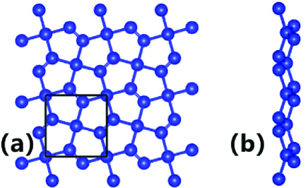
The penta-graphene can be considered as a sandwich structure, with the 4-coordinated C atoms sandwiched between the 3-coordinated atoms, and the schematic structure is plotted in Figure 1. Firstly, the lattice constants of CCC are optimized (==3.639 ), which is very close to previous theoretical valuesw1 . The elastic stiffness coefficients and piezoelectric stress tensors are calculated, and then can be attained. By using FDM, we obtain =271.84 =-20.86 and =153.15 . The calculated agree well with previous onesw1 . The is negative, which means a negative Poisson’s ratio. These related data are listed Table 1. For 2D materials, a pure out-of-plane piezoelectric response, compatible with the nowadays bottom/top gate technologies, is highly desired. For CCC monolayer, only out-of-plane piezoelectric response exits, but the predicted piezoelectric coefficient is very small, and the calculated value: =-0.099 C/m and =-0.065 pm/V. Some strategies should be applied to improve piezoelectric effect of CCC monolayer, and that only out-of-plane piezoelectric response holds.
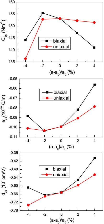
It has been proved that strain can effectively improve the piezoelectric response of 2D materials, such as r1 , AsPr2 , SnSer2 and Janus TMD monolayersr3 . For example, the of SnSe monolayer at -3.5% strain along the armchair direction is up to 628.8 pm/V from unstrained 175.3 pm/Vr2 . Here, the small both biaxial and uniaxial strain (-4% to 4%) effects on piezoelectric properties of monolayer CCC are investigated. The elastic constants , piezoelectric coefficients and as a function of strain are plotted in Figure 2. With both biaxial and uniaxial strains changing from -4% to 4%, both and show a non-monotonic behavior. It is found that, according to Equation 5, the compressive strain is in favour of improving piezoelectric response due to reducing and improving (absolute value). However, the enhancement is very small, and at -2% biaxial (-4% uniaxial) strain, the becomes -0.067 (-0.074 ) pm/V from unstrained -0.065 pm/V, increased only by 3.1% (13.9%).
IV Piezoelectric properties of CCB monolayer
A pentagonal CBB monolayer has also been predictedw2 , which can also be viewed as a B-C-B sandwich trilayer. In other words, the C atoms of the first and third layers of penta-graphene are replaced by B atoms. The symmetry still holds for CBB monolayer, and our optimized lattice constants ==3.933 , which agrees well with previous onesw2 . The calculated piezoelectric coefficients are =-0.372 C/m and =-0.418 pm/V, which are very larger than ones of CCC monolayer. However, our calculated elastic stiffness coefficients (=86.78 , =87.86 and =89.20 ) violate the Born criteria of mechanical stabilityela1 ; ela :
| (6) |
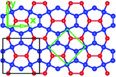
Experimentally, Janus TMD monolayer MoSSe with sandwiched S-Mo-Se structure has been synthesized by replacing the top S atomic layer in with Se atomsq8 . Thus, it is possible to build CCB monolayer by replacing the top C (B) atomic layer in monolayer CCC (CBB) with B (C) atoms. The schematic structure of CCB monolayer is shown in Figure 3. The symmetry of CCB monolayer reduces to (space group number 35), and the corresponding point group is . The Equation 3 changes into:
| (7) |
Here, the and are derived by Equation 7:
| (8) |
| (9) |
Fortunately, the CCB monolayer also possesses only out-of-plane piezoelectric effect. These also imply that the piezoelectric effects of CCB monolayer can be induced with a uniaxial strain being applied along x or/and y direction, which is different monolayer CCC and CBB with shear strain.

Compared with tetragonal structure of CCC and CBB, the crystal structure of CCB changes into orthorhombic, and the optimized lattice constants ==3.771 and =92.107. To confirm the dynamic stability of CCB monolayer, the phonon spectrum are calculated by VASP+Phonopy code with a supercell of 441 using the finite displacement methodpv5 . Figure 4 shows the calculated phonon spectrum. Although there are some negligibly small imaginary frequencies near the G point due to calculation error, no imaginary frequencies in the other q points throughout the Brillouin zone are observed, which implies the dynamic stability of CCB monolayer. The mechanical stability of CCB monolayer can be examined by elastic constants . The calculated =142.36 , =193.07 , =34.40 and =61.71 , which satisfy the Born criteria of mechanical stabilityela1 ; ela . The Young’s modulus and Poisson’s ratio as a function of in-plane can be attained on the basis of the elastic constants, as followsela1 :
| (10) |
| (11) |
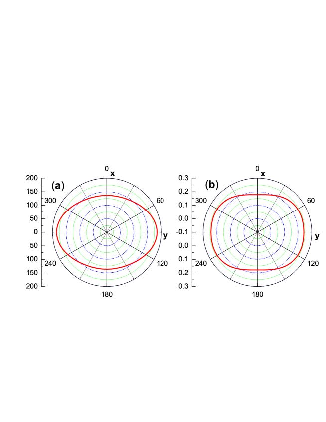
In which and . We show the calculated and in Figure 5. Both the Young’s modulus and Poisson’s ratio show mechanical anisotropy. According to calculated , CCB monolayer is softer along the x than y direction, which is due to B-B bond along x direction and C-C bond along y direction. A high Young’s modulus implies that the material is rigid, and the calculated results show that strain can easily tune it’s physical properties along x direction. It is found that the Poisson’s ratio along x direction (0.179) is smaller than one along y direction (0.242).
| Carrier type | () | (eV) | () | (s) | ||
|---|---|---|---|---|---|---|
| Electrons | x | 136.23 | 1.57 | 5.00 | 91.92 | |
| y | 184.76 | 0.42 | -1.15 | 8865.23 | ||
| Holes | x | 136.23 | -0.45 | -9.20 | 114.63 | |
| y | 184.76 | -1.02 | 6.97 | 118.75 |
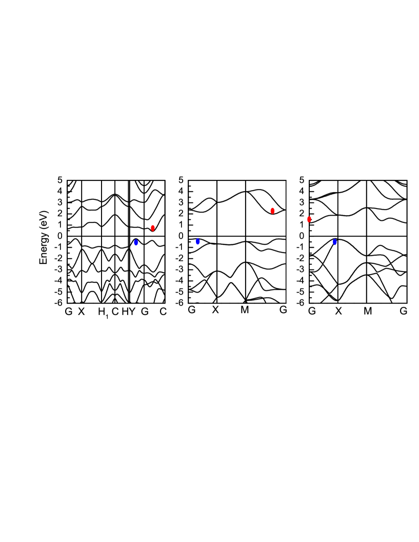
A 2D material with piezoelectricity not only should break inversion symmetry, but also has a band gap. The energy band structures of CCB along with CCC and CBB are plotted in Figure 6. It is clearly seen that CCB is an indirect band-gap semiconductor with a band gap of 0.66 eV, which is smaller than indirect gap 2.20 eV of CCC or 1.41 eV of CBB. The valance band maximum (VBM) lies on the G-Y path, while the conduction band minimum (CBM) is located on the G-C path. In fact, the valance band extrema (VBE) along G-X path is very close to VBM due to being very close to 90, and the difference is less than 1 meV. The carrier mobility of a semiconductors is an important factor for the application of electron device. The carrier mobility of a 2D material () by the deformation potential (DP) theory proposed by Bardeen and Shockleydp is defined as:
| (12) |
where , and () are the temperature, the effective mass in the transport direction and the average effective mass. The is the Young’s modulus derived from elastic constants . In addition, is the DP constant defined by () , where is the energy shift of the band edge of CBM or VBM with respect to the vacuum level after applying uniaxial strain. After attaining , the relaxation time can be attained by:
| (13) |
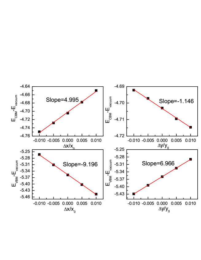
According to DP theory, the rectangular supercell is used to calculate carrier mobilities of monolayer CCB along the x and y directions in Figure 3. The calculated effective masses for electrons (CBM) and holes (VBM) with GGA are shown in Table 3. The band energies of the VBM and CBM with respect to the vacuum energy as a function of and are plotted in Figure 7, and the DP constant is calculated by linearly fitting these data. The carrier mobility and relaxation time for the electrons and holes of monolayer CCB on the basis of the calculated effective mass, elastic constant, and deformation potential constant are calculated along x and y directions at 300 K, which are summarized in Table 3. It is found that the electron mobility along y direction (8865.23 ) is almost 97 times larger than that along x direction (91.92 ). However, the hole mobilities along both x (114.63 ) and y (118.75 ) directions are very low, which is close to electron mobility along x direction.
In fact, the CCB is a representative Janus monomlayer. The asymmetric along the z direction with respect to central C atomic layer results in an out-of-plane piezoelectricity. However, mirror symmetry along x and y directions gives rise to disappeared in-plane piezoelectricity. This means that an in-plane stress or strain can only induce a polarization change vertical to the plane. Based on calculated and , the out-of-plane piezoelectric strain coefficient and can be attained, and the corresponding values are -0.505 pm/V and 0.273 pm/V, respectively. The out-of-plane is obviously higher than out-of-plane ones of many other 2D materials, such as functionalized h-BN (0.13 pm/V)y1 , MoSSe (0.29 pm/V)q7-2 , SbTeI (-0.37 pm/V)q7-2-1 , MoSTe (0.4 pm/V)q7-1 , Janus group-III materials (0.46 pm/V)y2 and - (0.415 pm/V)y3 . It is lower than one of BiTeI (-0.66 pm/V)q7-2-1 , (0.78 pm/V)y4 or (0.65 pm/V)y4 . However, the monolayer BiTeI, or not only has out-of-plane piezoelectricity, but also has in-plane piezoelectricity. Some related data are summarized in Table 2. Although the (CCC monolayer) and or (CCB monolayer) are all related to the out-of-plane piezoelectric effects, they are obviously different. The represents the piezoelectric response between the out-of-plane polarization and the in-plane shearing deformation, while or is referred to as the coupling between the out-of-plane polarization and the in-plane normal strain.
V Conclusion
In summary, the related piezoelectric effects of CCC monolayer are studied by using reliable first-principles calculations. Due to special symmetry for CCC monolayer, only out-of-plane exists, but it is very small. Firstly, we use both biaxial and uniaxial strains to tune piezoelectric properties of CCC monolayer. At -2% biaxial (-4% uniaxial) strain, the is increased only by 3.1% (13.9%), and the enhancement is very small. Inspiring from the already synthesized MoSSe monolayer, a Janus CCB monolayer with dynamic and mechanical stability is constructed, and the asymmetric along the z direction and mirror symmetry along x and y directions induce pure out-of-plane piezoelectricity. It is also found that CCB monolayer is a semiconductor, which is necessary for piezoelectric application. The calculated and are -0.505 pm/V and 0.273 pm/V, respectively, and the out-of-plane piezoelectric effect are obviously improved, compared with of CCC monolayer. The out-of-plane piezoelectricity of CCB monolayer is higher compared with other many 2D known materials. The very high room-temperature electronic mobility (8865.23 ) along y direction is predicted, which is very higher than that of Si (about 1400 ). Our works not only supply an experimental proposal for achieving large pure out-of-plane piezoelectric effect , but also offer an insight into piezoelectric effect of penta-graphene.
Acknowledgements.
This work is supported by the Natural Science Foundation of Shaanxi Provincial Department of Education (19JK0809). We are grateful to the Advanced Analysis and Computation Center of China University of Mining and Technology (CUMT) for the award of CPU hours and WIEN2k/VASP software to accomplish this work.References
- (1) S. Zhang, J. Zhou, Q. Wang, X. Chen, Y. Kawazoe and P. Jena, Proc. Natl. Acad. Sci. Unit. States Am. 112, 2372 (2015).
- (2) F. Li, K. Tu, H. Zhang and Z. Chen, Phys. Chem. Chem. Phys. 17, 24151 (2015).
- (3) Y. Ma, L. Kou, X. Li, Y. Dai and T. Heine, NPG Asia Mater. 8, e264 (2016).
- (4) J. Li, X. Fan, Y. Wei, H. Liu, S. Li, P. Zhao and G. Chen, Sci. Rep. 6, 33060 (2016).
- (5) H. Sun, S. Mukherjee and C. V. Singh, Phys. Chem. Chem. Phys. 18, 26736 (2016).
- (6) F. Q. Wang, J. Yu, Q. Wang, Y. Kawazoe and P. Jena, Carbon 105, 424 (2016).
- (7) W. Xu, G. Zhang and B. Li, J. Chem. Phys. 143, 154703 (2015).
- (8) J. Sun, Y. G. Guo, Q. Wang and Y. Kawazoe, Carbon 145, 445 (2019).
- (9) L. L. Liu, Y. Wang, C. P. Chen, H. X. Yu, L. S. Zhao and X. C. Wang, RSC Adv. 7, 40200 (2017).
- (10) W. Wu and Z. L. Wang, Nat. Rev. Mater. 1, 16031 (2016).
- (11) W. Wu, L. Wang, Y. Li, F. Zhang, L. Lin, S. Niu, D. Chenet, X. Zhang, Y. Hao, T. F. Heinz, J. Hone and Z. L. Wang, Nature 514, 470 (2014).
- (12) H. Zhu, Y. Wang, J. Xiao, M. Liu, S. Xiong, Z. J. Wong, Z. Ye, Y. Ye, X. Yin and X. Zhang, Nat. Nanotechnol. 10, 151 (2015).
- (13) A. Y. Lu, H. Zhu, J. Xiao, C. P. Chuu, Y. Han, M. H. Chiu, C. C. Cheng, C. W. Yang, K. H. Wei, Y. Yang, Y. Wang, D. Sokaras, D. Nordlund, P. Yang, D. A. Muller, M. Y. Chou, X. Zhang and L. J. Li, Nat. Nanotechnol. 12, 744 (2017).
- (14) L. Dong, J. Lou and V. B. Shenoy, ACS Nano, 11, 8242 (2017).
- (15) M. N. Blonsky, H. L. Zhuang, A. K. Singh and R. G. Hennig, ACS Nano, 9, 9885 (2015).
- (16) R. X. Fei, We. B. Li, J. Li and L. Yang, Appl. Phys. Lett. 107, 173104 (2015)
- (17) K. N. Duerloo, M. T. Ong and E. J. Reed, J. Phys. Chem. Lett. 3, 2871 (2012).
- (18) Y. Chen, J. Y. Liu, J. B. Yu, Y. G. Guo and Q. Sun, Phys. Chem. Chem. Phys. 21, 1207 (2019).
- (19) X. Wu, D. Vanderbilt and D. R. Hamann, Phys. Rev. B 72, 035105 (2005).
- (20) P. Hohenberg and W. Kohn, Phys. Rev. 136, B864 (1964); W. Kohn and L. J. Sham, Phys. Rev. 140, A1133 (1965).
- (21) G. Kresse, J. Non-Cryst. Solids 193, 222 (1995).
- (22) G. Kresse and J. Furthmller, Comput. Mater. Sci. 6, 15 (1996).
- (23) G. Kresse and D. Joubert, Phys. Rev. B 59, 1758 (1999).
- (24) J. P. Perdew, K. Burke and M. Ernzerhof, Phys. Rev. Lett. 77, 3865 (1996).
- (25) N. Jena, Dimple, S. D. Behere and A. D. Sarkar, J. Phys. Chem. C 121, 9181 (2017).
- (26) S. D. Guo, X. S. Guo, Y. Y. Zhang and K. Luo, arXiv:1910.08700 (2019).
- (27) Dimple, N. Jena, A. Rawat, R. Ahammed, M. K. Mohanta and A. D. Sarkar, J. Mater. Chem. A 6, 24885 (2018).
- (28) E. Cadelano, P. L. Palla, S. Giordano and L. Colombo, Phys. Rev. B 82, 235414 (2010).
- (29) R. C. Andrew, R. E. Mapasha, A. M. Ukpong and N. Chetty, Phys. Rev. B 85, 125428 (2012).
- (30) A. Togo, F. Oba, and I. Tanaka, Phys. Rev. B 78, 134106 (2008).
- (31) S. Bruzzone and G. Fiori, Appl. Phys. Lett. 99, 222108 (2011).
- (32) A. A. M. Noor, H. J. Kim and Y. H. Shin, Phys. Chem. Chem. Phys. 16, 6575 (2014).
- (33) S. D. Guo, X. S. Guo, R. Y. Han and Y. Deng, Phys. Chem. Chem. Phys. (2019). DOI: 10.1039/C9CP04590B.
- (34) S. D. Guo, X. S. Guo, Z. Y. Liu, Y. N. Quan, arXiv:1909.13227 (2019).
- (35) M. Yagmurcukardes, C. Sevik and F. M. Peeters, Phys. Rev. B 100, 045415 (2019).
- (36) Y. Guo, S. Zhou, Y. Z. Bai, J. J. Zhao, Appl. Phys. Lett. 110, 163102 (2017).
- (37) L. Hu and X. R. Huang, RSC Adv. 7, 55034 (2017).
- (38) J. Tan, Y. H. Wang, Z. T. Wang et al., Nano Energy 65, 104058 (2019).