Experimental Measurements of Effective Mass in Near Surface InAs Quantum Wells
Abstract
Near surface indium arsenide quantum wells have recently attracted a great deal of interest since they can be interfaced epitaxially with superconducting films and have proven to be a robust platform for exploring mesoscopic and topological superconductivity. In this work, we present magnetotransport properties of two-dimensional electron gases confined to an indium arsenide quantum well near the surface. The electron mass extracted from the envelope of the Shubnikov-de Haas oscillations shows an average effective mass = 0.04 at low magnetic field. Complementary to our magnetotransport study, we employed cyclotron resonance measurements and extracted the electron effective mass in the ultra high magnetic field regime. Both regimes can be understood by considering a model that includes non-parabolicity of the indium arsenide conduction bands.
.1 I. Introduction
Wafer-scale methods for the epitaxial growth of thin films of Aluminum (Al) on Indium Arsenide (InAs) heterostructures have recently been developed which yield uniform and atomically flat interfaces Wickramasinghe et al. (2018); Shabani et al. (2016); Lee et al. (2019a); Pauka et al. (2019). Josephson junctions fabricated on these materials yield a gate-controllable supercurrent with highly transparent contacts between the Al top layer and an InAs quantum well (QW) directly below the surface Kjaergaard et al. (2017); Suominen et al. (2017); Mayer et al. (2019); Lee et al. (2019b); Nichele et al. (2017). Tuning of the semiconductor properties will affect supercurrent and other superconducting properties due to the wavefunction overlap at the epitaxial interface. Josephson junctions made out of Al-InAs have been used for tunable superconducting qubits, the so-called “gatemon” where the Josephson energy can be tuned in-situ with an applied electric field Larsen et al. (2015); Casparis et al. (2018). Furthermore, since InAs has large spin-orbit coupling, they can host topological superconductivity and Majorana bound states Mayer et al. (2019, 2020); Ren et al. (2019); Fornieri et al. (2019). The key feature in these structures is that the two-dimensional electron gases (2DEG) is confined near the surface, in close proximity to the superconductor. While the epitaxial interface creates high contact transparency, it is expected that electron mobility of the 2DEG deteriorates due to increased rates of surface scattering as compared to isolated 2DEGs buried beneath the surface Wickramasinghe et al. (2018); Hatke et al. (2017); Ma et al. (2017). The myriad of possible applications with this platform implores a deeper study of the characteristics and material properties for near surface InAs QWs. In this work, the transport experiments investigate the isolated semiconductor with the superconducting layer removed and the optical measurements are conducted on the semiconductor samples which did not have a superconducting layer to begin with.
Two important material parameters of a 2DEG are the effective mass, , and the effective factor, . These parameters dictate the response of a material to external electric and magnetic fields. Their effect on device performance should be accounted for in the design of mesoscopic devices and realistic theoretical modeling. Both and have been measured and calculated for bulk InAs Madelung (2004) and for InAs QWs Yang et al. (1993a); Pryor and Pistol (2005). It is of particular interest that confinement of the electron wave function can strongly affect these values. Confinement becomes relevant when the 2DEG is placed near the surface, as is required for epitaxial contacts. In addition, narrow gap semiconductors can lead to strong non-parabolicity of the bands modifying the and . However, to date, very few experimental studies have been performed to quantify the and in near surface InAs quantum wells. Here we report on these properties using Shubnikov-de Haas (SdH) oscillations and cyclotron resonance (CR) technique.
.2 II. Sample Growth and Preparation
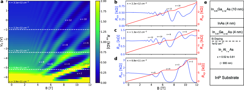
The samples were grown on a semi-insulating InP (100) substrate, using a modified Gen II molecular beam epitaxy system. The InxAl1-xAs buffer is grown at low temperature to help mitigate formation of dislocations originating from the lattice mismatch between the InP substrate and higher levels of the heterostructure Wallart et al. (2005); Shabani et al. (2014a, b). The indium content of InxAl1-xAs is step-graded from 0.52 to 0.81. Next, a delta-doped Si layer of cm-2 density is placed here followed by 6 nm of In.81Al.19As. The quantum well is grown next, consisting of a 4 nm thick layer of In0.81Ga0.19As layer, a 4 nm thick layer of InAs, and finally a 10 nm thick top layer of In0.81Ga0.19As. A thin film of Al can be epitaxially grown on the final InGaAs layer. For the transport studies of the InAs quantum wells, Al films were selectively etched by Transene type-D solution while for optical studies Al was not grown from the beginning.
.3 III. Device Fabrication and Measurement Setup
The samples used for our transport measurements were patterned using photolithography. The pattern used was an L-shaped Hall bar geometry allowing simultaneous measurement of longitudinal resistances ( and ) and transverse resistance (). Chemical wet etching was performed after lithographic patterning leaving a 900 nm tall mesa. A 50 nm thick aluminum oxide (Al2O3) gate dielectric was then deposited on top of the Hall bar via atomic layer deposition. Gate electrodes were realized by subsequent deposition of 5 nm of titanium and 70 nm of gold. All measurements were performed inside a cryogen-free refrigerator with base temperature of 1.5 K with maximum magnetic field of 12 T. Carrier densities are determined based on the slope of Hall data.
.4 IV. Measurement Results
.5 A. Magnetotransport Measurements
Figure 1a shows the color-scale plot of longitudinal magnetotransport, , as a function of top gate voltage, . The Landau level fan diagram is evident from the plot with crossings observed at near cm-2 and 8 T and another near cm-2 and 12 T. At lowest densities we only observe well developed integer quantum Hall states up to cm-2 ( -3 V). The first Landau level crossing appears near -3 V where it signals occupation of the second electric subband. This is most evident as = 6 stays the same before and after the crossing in Fig. 1a. Similar Landau level crossings have been studied extensively in GaAs 2DEGs Muraki et al. (2001); Ellenberger et al. (2006); Zhang et al. (2005); Liu et al. (2011). Three magnetotransport traces are shown in Fig. 1b-d. Longitudinal and Hall resistance as a function of magnetic field are plotted for , , and cm-2. The beating in SdH oscillations clearly suggest occupation of two subbands at cm-2 where below the crossing clear quantum Hall states develop with vanishing longitudinal resistance at .
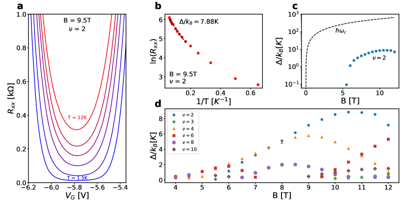
In a non-interacting quantum Hall system, the Landau level spacing increases with magnetic field as with where B is the magnetic field, and is the bare electron mass. Hence, measurements of energy gaps of integer quantum Hall states should be related to electron mass. Figure 2a shows the temperature dependence of longitudinal resistance as a function of gate voltage near the filling factor = 2 and at the magnetic field 9.5 T. The natural logarithm of the minimum in resistance in a system with parabolic bands has a linear dependence on inverse temperature as shown in Fig. 2b Mani et al. (2002). The energy gap is directly proportional to the magnitude of the slope. We repeated these measurements as we varied the density and hence the position of = 2 in magnetic field. The results are shown in Fig. 2c where extracted energy gaps are plotted as a function of magnetic field. For comparison, we also plot the energy gap expected from as a black dashed line. There is a large discrepancy between the measured and expected energy gap. If we allow electron mass to be a fitting parameter we obtain unrealistically high values of for electrons. We have also studied the energy gaps of filling factors = 3, 4, 6, 8, 10. Figure 2d shows the energy gaps are between 0-10 K. All these values are much smaller than their corresponding . The energy gaps for each filling factor first increase with magnetic field, then decrease, and eventually disappear near the Landau level crossings. For odd integer quantum Hall states, the Landau levels are split by the Zeeman energy . Our data indicates that odd integers are mainly absent and only begin to develop at higher magnetic field ( = 3 near 12 T) as shown in Fig. 1a. Given the bulk g-factor in InAs (g = -14), the odd integers should have large enough energy gaps to be clearly observed. Their very weak presence is due to either modified or Landau level broadening due to disorder. To address this and the discrepancy of energy scales for gaps in even integer quantum Hall states we next measure the temperature dependence of the low magnetic field SdH oscillations where only free electrons contribute to the transport.
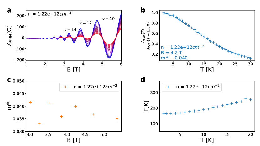
The SdH oscillation amplitude can be isolated by subtracting the background trend of the longitudinal resistance . Figure 3a displays the amplitude of SdH, for a carrier density of . Taking the points for a single minimum or maximum, normalized by our lowest temperature value, we can fit them to the formula with , where T is the temperature and E is the gap. This allows us to calculate . Figure 3b shows the data and fit for the oscillation near B = 4.2 T from 3a. We have repeated these measurements for various filling factors to extract as shown in 3c. The experimental values range between 0.035 - 0.05 with an average value near = 0.04. This is slightly higher than bulk values of our quantum well consisting of InAs and In0.81Ga0.19As with = 0.023 and 0.03 respectively. From the exponential envelope of the SdH oscillations we can also obtain the quantum lifetime and calculate the Landau level broadening, . Figure 3d shows for carrier density n = 1.22 cm-2. The Landau level broadening range is around 200 K for cm-2. The broadening in the near surface InAs 2DEG is significantly larger than in buried InAs 2DEGs where is measured to be 5 K Shabani et al. (2014b). Here the surface scattering clearly dominates the other scattering mechanisms Wickramasinghe et al. (2018). Thankfully, the smaller electron mass in InAs enhances the energy scales and therefore enables us to resolve quantum Hall states. Our measured Landau level broadening could qualitatively describe the large discrepancy between energy gap measurements in the quantum Hall states and .
.6 B. Cyclotron Resonance Measurements
A more direct way to measure is through infrared CR measurements using pulsed ultrahigh magnetic fields ( 150 Tesla) generated by the single-turn coil technique Sanders et al. (2003); Khodaparast et al. (2013); Sun et al. (2015). The external pulsed magnetic field was applied along the growth direction and measured by a pick-up coil around the sample. The sample and the pick-up coil were placed inside a continuous flow helium cryostat. In this study, we employed infrared radiations from a CO2 laser with wavelengths ranging from 9.2-10.6 m. The sample in this measurement has a density of cm-2. The changes in transmission through the sample were collected using a fast liquid-nitrogen-cooled HgCdTe detector. A multi-channel digitizer placed in a shielded room recorded the signals from the detector and pick-up coil.
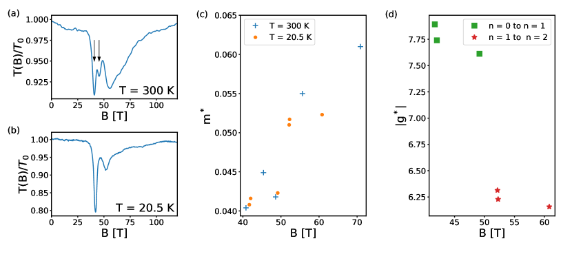
The spin resolved CR at 10.6 m indicated by the two arrows in Fig. 4a, separated by 4 Tesla, was observed at T = 300 K. This fact can be expected, as the Landau levels above the Fermi level can be occupied at T = 300 K, allowing the transitions between n = 0 and n = 1 for two different spins. In addition, in Fig. 4a the broad resonance at 55 T represents a transition between n = 1 and n = 2 which is possible when the carrier lifetime allows time for a finite population of Landau level n = 1. This transition is not predicted from the fixed Fermi energy, but can be attributed to the non-equilibrium electron distribution Khodaparast et al. (2004); Yang et al. (1993b).
In Fig. 4b, we present the CR measurements at 20.5 K with an excitation of 10.6 m. The spin resolved CR was not observed indicating the states above the Fermi energy are no longer occupied. On the other hand, the broad resonance observed at 55 T and T = 300 K, which is due to the transition from n = 1 to n = 2, remained and narrowed. Figure 4c summarizes our measurements for as a function of magnetic field at T = 300 K (crosses) and T = 20.5 K (filled circles). We note that although the single-turn coil is destroyed in each shot, the sample and pick-up coil remain intact, making it possible to carry out temperature and wavelength dependence measurements on the same sample. Figure 4c shows that the varied and increased monotonically with magnetic field. We measured = 0.04 near B = 40 T and = 0.061 near 70 T. Correspondingly we can estimate as a function of magnetic field using appropriate Landau level index using Eq. 1. In Fig. 4d we present absolute effective g-factor at 20.5 K as a function of magnetic field.
.7 V. Landau Level Modeling
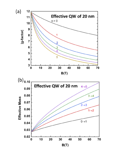
Next we provide a simple theoretical model to understand and the Landau level fan diagram in InAs which has a non-parabolic conduction band. Unlike the wide gap semiconductors such as GaAs, CR and may vary with subband index, Landau Level index, and external magnetic field. Beginning with expectations from the bulk and introducing confinement we can arrive at expressions for and (the details are presented in the Appendix):
| (1) |
where is the energy of the Landau level, for the subband index, and at magnetic field . Plus and minus superscripts represent higher and lower Zeeman split energy bands respectively. As shown in Fig. 5a, depends on the subband index , the Landau level as well as the magnetic field . At zero magnetic field, the absolute value of = 12 is reduced from bulk value of = 14 due to confinement and monotonically decreases as magnetic field is increased. The rate depends on the Landau level index.
Similarly one can define obtained by CR as:
| (2) |
We find that , as shown in Fig. 5b also depends on the Landau level, the subband index, and the magnetic field (we plot only the () solution for clarity). At zero magnetic field we see = 0.027 is larger than the bulk value of = 0.023 and increases monotonically as magnetic field is increased. These values are in close agreement with values derived from magnetotransport (over a small region 3 T to 5 T) and CR (40 T B 70 T).
.8 VI. Conclusion
We have done magnetotransport and ultra high field cyclotron resonance characterization of surface InAs Quantum wells. The density of these structures can be tuned and our magnetotransport measurement provides insight into the Landau level broadening and the quantum Hall energy gaps. By combining magnetotransport and cyclotron resonance measurements we can obtain conduction band effective mass at both low and high magnetic fields respectively. A band structure model which includes the effects of strong non-parabolicity and quantum confinement can describe the extracted from magnetotransport and cyclotron resonance measurements. We used our experimental CR values to determine the effective g-factor as a function of magnetic fields and Landau level index and these values are in a good agreement with the model presented here.
Acknowledgment: The NYU team acknowledges partial support from U.S. Army Research Office agreements W911NF1810067 and W911NF1810115. and NSF Grants No. NSF-MRSEC 1420073 and No. NSF DMR - 1702594. G.A.K. and C.J.S. acknowledge support from the Air Force Office of Scientific Research under Award No. FA9550-17-1-0341. G.A.K. and B.A.M. acknowledge support from the Japanese visiting program of The Institute for Solid State Physics, The University of Tokyo. J.Y. acknowledges funding from the ARO/LPS QuaCGR fellowship reference W911NF1810067.
I Appendix: Simple model for electron mass and g-factor in a non-parabolic semiconductor.
The derivation of the theoretical model accounting for non-parabolicity is described in this section. In the absence of external magnetic field (and quantum confinement) a narrow gap semiconductor such as InAs has a conduction band energy, vs. wavevector given by the dispersion relationship is given by:
| (3) |
Here, is the non-parabolicity factor given by
| (4) |
with being the band-gap, and is the CR at the band edge (). For small , the energy depends quadratically on while for large , the energy depends linearly on .
In the presence of a magnetic field in the direction, it can be shown Mavroides (1972); Lax and Mavroides (1960); Bowers and Yafet (1959) that one can write:
| (5) |
Here, is the Landau level index which can take on values [0,1,2,…]. is the band-edge CR frequency, given by:
| (6) |
and
| (7) |
is the band-edge . is the valence band spin-orbit splitting, and is the Bohr-magneton given by:
| (8) |
Note that in the Bohr magneton, as opposed to the band-edge CR frequency, it is the bare electron mass that enters the expression.
To simplify, we set the RHS of Eq. 5 to
| (9) |
and then solve for the energy .
| (10) |
The plus sign corresponds to the conduction band while the minus sign corresponds to the light hole in the valence bands. Quantum confinement will also affect both and for narrow gap materials. To take into account quantum confinement, one quantizes as:
| (11) |
with a positive integer and the effective width of the quantum well. Substituting into equation 5 yields:
| (12) |
We assume an effective well width of 20 . The gap at low temperatures is given by while the spin orbit splitting is eV and the low temperature, band-edge effective mass is: . From Eq. 7, we see this yields a band-edge .
The Landau fan energies in Eq. 12 can lead us to calculate and define for different Landau levels by:
| (13) |
We can see that depends on the subband index , the Landau level as well as the magnetic field .
Similarly one can define by:
| (14) |
Figure 5(a,b) plots the and as a function of magnetic field and the Landau level index. We plot only for the lowest (-) solution. Since will differ between Landau levels for a non-parabolic system. The + and - effective masses will differ slightly and will lead to spin-split cyclotron resonance peaks under certain conditions. The calculation shows that in presence of non-parabolicity both of these parameters depend on the subband index , the Landau level , and the magnetic field . We note that assuming a smaller effective quantum well width (e.g. 12 nm) will shift to larger values (e.g. 0.035 at B = 0 T) and will shift smaller values ( -9.5 at B = 0 T).
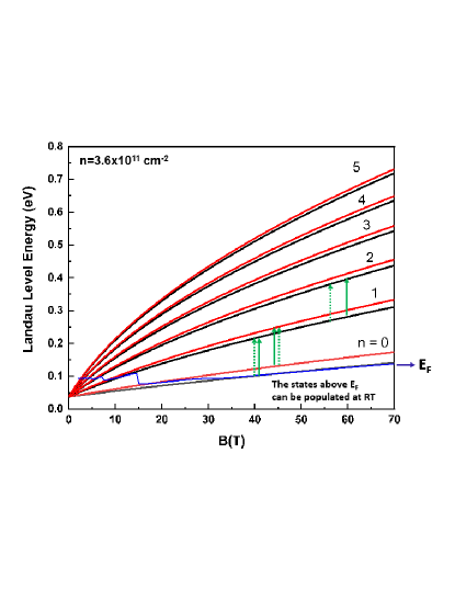
As shown in Fig. 6, we have also calculated the Landau levels for the 1st subband. With the effective g-factor being negative, Red lines are spin down, Blacks are spin up. The solid green arrows indicate the predicted CR transitions at 10.6 and are in close agreement with experimental observations indicated by dashed green arrows. While in the theory presented here, we considered the infinite potential well, the agreement between the theory and experiment is better at lower magnetic fields. We should note that the Fermi level can be occupied at T = 300 K, allowing transitions between n = 0 and n = 1 for two different spins. The spin resolved CR was not allowed at lower temperatures and the resonances above 50 T, in Fig.4a and Fig.4b are attributed to the transitions between n = 1 and n = 2 . These transitions are possible where the photo-excited carrier lifetime is long enough to populate the Landau level n = 1, even though the position of the Fermi level would not predict the transitions.
References
References
- Wickramasinghe et al. (2018) K. S. Wickramasinghe, W. Mayer, J. Yuan, T. Nguyen, L. Jiao, V. Manucharyan, and J. Shabani, Applied Physics Letters 113, 262104 (2018).
- Shabani et al. (2016) J. Shabani, M. Kjaergaard, H. J. Suominen, Y. Kim, F. Nichele, K. Pakrouski, T. Stankevic, R. M. Lutchyn, P. Krogstrup, R. Feidenhans’l, et al., Phys. Rev. B 93, 155402 (2016).
- Lee et al. (2019a) J. S. Lee, B. Shojaei, M. Pendharkar, M. Feldman, K. Mukherjee, and C. J. Palmstrøm, Phys. Rev. Materials 3, 014603 (2019a), URL https://link.aps.org/doi/10.1103/PhysRevMaterials.3.014603.
- Pauka et al. (2019) S. J. Pauka, J. D. S. Witt, C. N. Allen, B. Harlech-Jones, A. Jouan, G. C. Gardner, S. Gronin, T. Wang, C. Thomas, M. J. Manfra, et al., arXiv:1908.08689 (2019).
- Kjaergaard et al. (2017) M. Kjaergaard, H. J. Suominen, M. P. Nowak, A. R. Akhmerov, J. Shabani, C. J. Palmstrøm, F. Nichele, and C. M. Marcus, Phys. Rev. Applied 7, 034029 (2017), URL https://link.aps.org/doi/10.1103/PhysRevApplied.7.034029.
- Suominen et al. (2017) H. J. Suominen, M. Kjaergaard, A. R. Hamilton, J. Shabani, C. J. Palmstrøm, C. M. Marcus, and F. Nichele, Phys. Rev. Lett. 119, 176805 (2017).
- Mayer et al. (2019) W. Mayer, J. Yuan, K. S. Wickramasinghe, T. Nguyen, M. C. Dartiailh, and J. Shabani, Applied Physics Letters 114, 103104 (2019).
- Lee et al. (2019b) J. S. Lee, B. Shojaei, M. Pendharkar, A. P. McFadden, Y. Kim, H. J. Suominen, M. Kjaergaard, F. Nichele, C. M. Marcus, and C. J. Palmstrom, Nano Lett. 19, 3083 (2019b).
- Nichele et al. (2017) F. Nichele, A. C. C. Drachmann, A. M. Whiticar, E. C. T. O’Farrell, H. J. Suominen, A. Fornieri, T. Wang, G. C. Gardner, C. Thomas, A. T. Hatke, et al., Phys. Rev. Lett. 119, 136803 (2017).
- Larsen et al. (2015) T. W. Larsen, K. D. Petersson, F. Kuemmeth, T. S. Jespersen, P. Krogstrup, J. Nygård, and C. M. Marcus, Phys. Rev. Lett. 115, 127001 (2015).
- Casparis et al. (2018) L. Casparis, M. R. Connolly, M. Kjaergaard, N. J. Pearson, A. Kringhøj, T. W. Larsen, F. Kuemmeth, T. Wang, C. Thomas, S. Gronin, et al., Nature Nanotechnology 13, 915 (2018), URL https://doi.org/10.1038/s41565-018-0207-y.
- Mayer et al. (2019) W. Mayer, M. C. Dartiailh, J. Yuan, K. S. Wickramasinghe, A. Matos-Abiague, I. Žutić, and J. Shabani, arXiv e-prints arXiv:1906.01179 (2019), eprint 1906.01179.
- Mayer et al. (2020) W. Mayer, M. C. Dartiailh, J. Yuan, K. S. Wickramasinghe, E. Rossi, and J. Shabani, Nature Communications 11, 212 (2020), URL https://doi.org/10.1038/s41467-019-14094-1.
- Ren et al. (2019) H. Ren, F. Pientka, S. Hart, A. T. Pierce, M. Kosowsky, L. Lunczer, R. Schlereth, B. Scharf, E. M. Hankiewicz, L. W. Molenkamp, et al., Nature 569, 93 (2019), URL https://doi.org/10.1038/s41586-019-1148-9.
- Fornieri et al. (2019) A. Fornieri, A. M. Whiticar, F. Setiawan, E. Portolés, A. C. C. Drachmann, A. Keselman, S. Gronin, C. Thomas, T. Wang, R. Kallaher, et al., Nature 569, 89 (2019).
- Hatke et al. (2017) A. T. Hatke, T. Wang, C. Thomas, G. Gardner, and M. Manfra, Appl. Phys. Lett. 111, 142106 (2017).
- Ma et al. (2017) M. K. Ma, M. S. Hossain, K. A. Villegas Rosales, H. Deng, T. Tschirky, W. Wegscheider, and M. Shayegan, Phys. Rev. B 96, 241301 (2017), URL https://link.aps.org/doi/10.1103/PhysRevB.96.241301.
- Madelung (2004) O. Madelung, Semiconductors: Data Handbook (Springer Berlin Heidelberg, 2004).
- Yang et al. (1993a) M. J. Yang, P. J. Lin-Chung, B. V. Shanabrook, J. R. Waterman, R. J. Wagner, and W. J. Moore, Phys. Rev. B 47, 1691 (1993a), URL https://link.aps.org/doi/10.1103/PhysRevB.47.1691.
- Pryor and Pistol (2005) C. E. Pryor and M.-E. Pistol, Phys. Rev. B 72, 205311 (2005), URL https://link.aps.org/doi/10.1103/PhysRevB.72.205311.
- Wallart et al. (2005) X. Wallart, J. Lastennet, D. Vignaud, and F. Mollot, Appl. Phys. Lett. 87, 043504 (2005).
- Shabani et al. (2014a) J. Shabani, A. P. McFadden, B. Shojaei, and C. J. Palmstrøm, Applied Physics Letters 105, 26 (2014a).
- Shabani et al. (2014b) J. Shabani, S. Das Sarma, and C. J. Palmstrøm, Phys. Rev. B 90, 161303 (2014b).
- Muraki et al. (2001) K. Muraki, T. Saku, and Y. Hirayama, Phys. Rev. Lett. 87, 196801 (2001), URL https://link.aps.org/doi/10.1103/PhysRevLett.87.196801.
- Ellenberger et al. (2006) C. Ellenberger, B. Simovič, R. Leturcq, T. Ihn, S. E. Ulloa, K. Ensslin, D. C. Driscoll, and A. C. Gossard, Phys. Rev. B 74, 195313 (2006), URL https://link.aps.org/doi/10.1103/PhysRevB.74.195313.
- Zhang et al. (2005) X. C. Zhang, D. R. Faulhaber, and H. W. Jiang, Phys. Rev. Lett. 95, 216801 (2005), URL https://link.aps.org/doi/10.1103/PhysRevLett.95.216801.
- Liu et al. (2011) Y. Liu, J. Shabani, and M. Shayegan, Phys. Rev. B 84, 195303 (2011), URL https://link.aps.org/doi/10.1103/PhysRevB.84.195303.
- Mani et al. (2002) R. G. Mani, J. H. Smet, K. von Klitzing, V. Narayanamurti, W. B. Johnson, and V. Umansky, Nature 420, 646—650 (2002), ISSN 0028-0836, URL https://doi.org/10.1038/nature01277.
- Sanders et al. (2003) G. D. Sanders, Y. Sun, F. V. Kyrychenko, C. J. Stanton, G. A. Khodaparast, M. A. Zudov, J. Kono, Y. H. Matsuda, N. Miura, and H. Munekata, Phys. Rev. B 68, 165205 (2003), URL https://link.aps.org/doi/10.1103/PhysRevB.68.165205.
- Khodaparast et al. (2013) G. A. Khodaparast, Y. H. Matsuda, D. Saha, G. D. Sanders, C. J. Stanton, H. Saito, S. Takeyama, T. R. Merritt, C. Feeser, B. W. Wessels, et al., Phys. Rev. B 88, 235204 (2013), URL https://link.aps.org/doi/10.1103/PhysRevB.88.235204.
- Sun et al. (2015) Y. Sun, F. V. Kyrychenko, G. D. Sanders, C. J. Stanton, G. A. Khodaparast, J. Kono, Y. H. Matsuda, and H. Munekata, SPIN 05, 1550002 (2015), eprint https://doi.org/10.1142/S2010324715500022, URL https://doi.org/10.1142/S2010324715500022.
- Khodaparast et al. (2004) G. Khodaparast, R. Meyer, X. Zhang, T. Kasturiarachchi, R. Doezema, S. Chung, N. Goel, M. Santos, and Y. Wang, Physica E: Low-dimensional Systems and Nanostructures 20, 386 (2004), ISSN 1386-9477, proceedings of the 11th International Conference on Narrow Gap Semiconductors, URL http://www.sciencedirect.com/science/article/pii/S1386947703004545.
- Yang et al. (1993b) M. J. Yang, R. J. Wagner, B. V. Shanabrook, J. R. Waterman, and W. J. Moore, Phys. Rev. B 47, 6807 (1993b), URL https://link.aps.org/doi/10.1103/PhysRevB.47.6807.
- Mavroides (1972) J. Mavroides, in Optical properties of solids. North Holland, Amsterdam pp. 351–528 (1972).
- Lax and Mavroides (1960) B. Lax and J. G. Mavroides, in Solid State Physics (Elsevier, Amsterdam, 1960), vol. 11, pp. 261–400.
- Bowers and Yafet (1959) R. Bowers and Y. Yafet, Physical Review 115, 1165 (1959).