Effect of tunneling on the electrical conductivity of nanowire-based films: computer simulation within a core–shell model
Abstract
We have studied the electrical conductivity of two-dimensional nanowire networks. An analytical evaluation of the contribution of tunneling to their electrical conductivity suggests that it is proportional to the square of the wire concentration. Using computer simulation, three kinds of resistance were taken into account, viz., (i) the resistance of the wires, (ii) the wire—wire junction resistance, and (iii) the tunnel resistance between wires. We found that the percolation threshold decreased due to tunneling. However, tunneling had negligible effect on the electrical conductance of dense nanowire networks.
I Introduction
Nanowire networks (NWNs) have excellent optical, electrical and mechanical performances, which makes them very attractive for use as transparent electrodes in modern photovoltaics, light-emitting devices, touch screens, and thin-film transparent heaters.Manning et al. (2019) These applications require high transmittance of transparent electrodes while their sheet resistance should be within different ranges.Bae et al. (2012); Manning et al. (2019) The required sheet resistance varies from 500 in the case of touch screens to 1 in the case of solar cells.Bae et al. (2012) To ensure quality wire-to-wire contacts, different methods of treatment are used, viz., annealing,Lee et al. (2008); Madaria et al. (2010) plasmonic welding,Garnett et al. (2012) laser nanowelding,Han et al. (2014) mechanical pressing,Tokuno et al. (2011) electroless-welding,Xiong et al. (2016) capillary force,Lee et al. (2013) the welding of crossed silver nanowires (AgNWs) by chemically growing silver “solder” at the junctions of the nanowires,Lu et al. (2015) capillary-force-induced cold welding,Liu et al. (2017) room-temperature plasma treatment,Zhu et al. (2013) electroplating welding,Zhao et al. (2019) and electrical activation under ambient conditions using current-induced local heating of the junction.Bellew et al. (2015) Depending on the initial resistance, by using these technologies,the sheet resistivity can be reduced by several orders of magnitude to tens of ohms.
Depending on the manufacturing technology, the diameter and length of AgNWs may be different. Ref. Lee et al., 2008 reported on AgNWs that were m long with a diameter of nm, i.e., the aspect ratio, , was approximately . In Ref. Nguyen et al., 2019, the AgNWs had an average diameter of nm and an average length of m, i.e., . In Ref. Bellew et al., 2015, m, nm, i.e., . In Ref. He et al., 2018, the mean length and diameter were m nm, respectively, i.e., . Ref. Lee et al., 2016 reported on well-defined AgNWs with a narrow diameter distribution, uniform, through the range of 16–22 nm, with a long dimension of up to m, i.e., . AgNWs of the same aspect ratio and lengths up to m have also been reported on in Ref. Xu et al., 2018. Thus, the aspect ratios of the AgNWs that have been considered range from 100 to 1000 in order of magnitude.
Four-probe measurements on almost 40 individual nanowires, with diameters ranging from 50 to 90 nm, gave an average resistivity of nm.Bellew et al. (2015) Junction resistance measurements of individual silver nanowire junctions have been performed and the distribution of junction resistance values presented.Bellew et al. (2015) The distribution of the junction resistance, determined using three different methods, showed a strong peak at 11 , corresponding to the median value of the distribution, and the presence of a small percentage (6%) of high-resistance junctions.Bellew et al. (2015) Thus, the junction resistance and the resistance of an individual wire are mostly of the same order. Helpfully, Ref. Bellew et al., 2015 also presents a synopsis of previously reported junction resistance values.
Different approaches have been applied to compute the electrical conductivity of NWNs, e.g., a percolation approach,Žeželj and Stanković (2012) an effective medium theory,O’Callaghan et al. (2016) a geometrical consideration,Kumar and Kulkarni (2016) and a kind of mean-field approximation (where transport within the system was described by the interaction of individual decoupled wires with a linear average potential background).Forró et al. (2018) A systematic analysis of the electrical conductivity of networks of conducting rods has recently been presented.Kim and Nam (2018)
Recently, percolating NWNs of widthless, stick nanowires have been considered.Benda, Cancès, and Lebental (2019) The effective resistance of such NWNs has been studied by taking into account the wire resistance, wire—wire contact resistance, and metallic electrode—wire contact resistance. An accurate closed-form approximation of the effective resistance based on the above physical parameters has been proposed.Benda, Cancès, and Lebental (2019)
An approximate analytical model for random NWN electrical conductivity has been proposed.Jagota and Scheinfeld (2019) This approach is faster than existing computational methods. The approach is based on the assumption that where means the expected value, is the sheet conductivity of a random NWN, and is the adjacency matrix of this NWN.
A computational method has been developed to investigate the electrical properties of a silver NWN.Han et al. (2018) This method is based on extraction of the electrically conductive backbones and accounting for the wire—wire junction resistance. An investigation has also been performed of how conductivity exponents depend on the ratio of the stick—stick junction resistance to the stick resistance for two-dimensional stick percolation.Li and Zhang (2010)
To characterize NWNs, the number density, , i.e., the number of wires, , per unit area, may be used.Mertens and Moore (2012) To mimic the shape of elongated particles and, at the same time, simplify connectivity simulations, different simple geometrical figures are used, e.g., sticks,Li and Zhang (2009) rectangles,Li and Östling (2013) ellipses,Li and Östling (2016) superellipses,Lin and Chen (2019) and stadia.Tarasevich and Eserkepov (2019) A stadium is a rectangle with semicircles at a pair of opposite sides [Fig. 1(a)]. Its aspect ratio is
| (1) |
A discorectangle (stadium) is the two-dimensional analog of a spherocylinder (a stadium of revolution or capsule), i.e., three-dimensional geometric shape consisting of a cylinder with hemispherical ends. When , the percolation thresholds for ellipses and rectangles are Li and Östling (2016) and ,Li and Östling (2013) respectively, while this value for zero-width sticks is .Li and Zhang (2009) In such a way, real-world AgNWs () can, in simulations, be treated as zero-width sticks.
Although the presence of a giant component ensures the electrical conductivity of NWNs above the percolation threshold, electrical conductivity may, in principle, also occur slightly below the percolation threshold due to tunneling.Balberg (2009) Moreover, tunneling may contribute to the electrical conductivity of NWNs even above the percolation threshold. In particular, there is an opinion that the conduction mechanism changes from tunneling to free electron conduction at increased AgNW concentration since the conductivity of the AgNWNs is mainly influenced by their surface and grain boundary scattering.Sohn et al. (2019) Naturally, there should be a range of concentrations where both the mechanisms are of approximately the same importance.
The tunnel conductivity between the two wires is defined as
| (2) |
where is the shortest distance between the -th and -th wires [Fig. 1(b)], is the conductivity of the junction between the two wires, while the tunneling decay length, , depends on the electronic potential barrier between the two wires.Ambrosetti et al. (2010); Nigro et al. (2013) In fact, (2) is a simplified notation of the Simmons’ formula.Simmons (1963); *Matthews2018JAP
Although the contribution of tunneling to the electrical conductivity of three-dimensional NWNs has been analyzed,Ambrosetti et al. (2010); Nigro et al. (2013); Nigro and Grimaldi (2014); Haghgoo et al. (2019) to the best of our knowledge, its contribution into the electrical conductivity of two-dimensional NWNs has not yet been fully studied. The goal of the present work was to obtain the dependencies of the electrical conductivity of NWNs on their junction resistances. Two kinds of junction are involved in the consideration, viz., contact junctions and tunnel junctions. The rest of the paper is constructed as follows. In Section II, the technical details of the simulations and calculations are described and some tests are presented. Section III presents our main findings. In Section IV, we summarize and discuss the main results.
II Methods
To simplify tunneling computations, the tunneling conductance is accounted only within the cutoff distance, .
| (3) |
The region within the cutoff distance is a stadium. In such a way, a wire consists of a core having the conductivity , and a stadium shaped shell that can result in tunnel conductivity when two shells overlap [Fig. 1(a)].
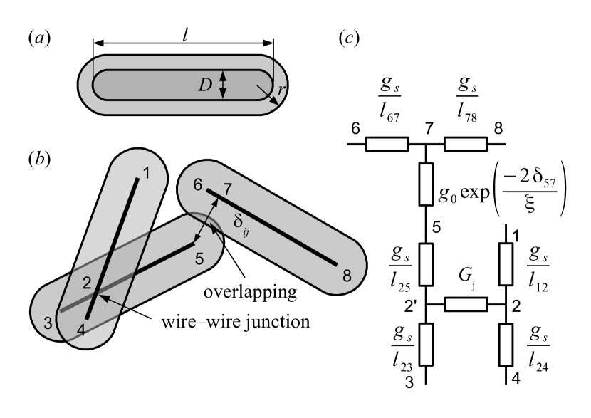
Wires with and were added one by one randomly, uniformly, and isotropically onto a substrate of size having periodic boundary conditions (PBCs), i.e., onto a torus, until a cluster spanning around the torus in two directions had arisen. Any two wires are supposed to be connected into one cluster when their shells (stadia) overlap each other [Fig. 1(b)]. was used in all our computations. Since in our case the area is , the desired number density is
| (4) |
We denote as the number density corresponding to the occurrence of a spanning cluster. We used the union—find algorithmNewman and Ziff (2000, 2001) to check for any occurrences of spanning clusters. In our study, we used a version of the union—find algorithm adapted for continuous percolation.Li and Zhang (2009); Mertens and Moore (2012) After the critical number density, , had been determined, wires continued to be added until the desired concentration was reached.
The electrical conductivity of the spanning cluster was calculated as follows. For calculation of the electrical conductance, the PBCs were removed, i.e., the torus was unrolled into a plane, and two conducting buses were applied to the opposite borders of the system. The electrical conductance was calculated between these buses. Within the spanning cluster, all intersections of the cores and all overlappings of the shells were identified. The nearest distance between the cores of two stadia with overlapping shells may be either between their ends or between a core end of one of the stadia and an intermediate point on the core of the second one. We treated the latter as tunnel junctions. Both points of core intersections (contact junctions) and tunnel junctions divide the cores into segments. Each segment of a core between two junctions and of any of the two kinds was considered as a conductance , where is the length of the segment. Each core intersection was considered as providing an additional conductance while the conductances of tunnel junctions were calculated according to Eq. (3). In such a way, an electrical circuit was produced for each spanning cluster [Fig. 1(c)]. Having this electrical circuit, Kirchhoff’s current law can be used for each junction of rods and Ohm’s law for each occurrence of conductivity between two junctions. The resulting set of equations was solved numerically to find the total conductance of the NWN. For each given number of deposited stadia, , independent runs were performed to obtain the electrical conductance.
In all our computations, the electrical conductivity of the core was fixed, viz., arb.u., while the tunnel electrical conductivity varied . We supposed that the case corresponds to untreated NWNs while corresponds to NWNs welded using the various technologies previously noted. Since the typical length of an AgNW is of the order m while the tunneling decay length is of the order m,Nigro et al. (2013); Ambrosetti et al. (2010) we put . Additionally, we studied the effect of the tunneling decay length on the electrical conductance for the ratios and . The cutoff distance and the tunneling decay length were connected as . The rationale for this choice is given in Section III.1.
The error bars are of the order of the marker size when not shown explicitly. Due to isotropy, the electrical conductances in the two perpendicular directions are the same within statistical error, thus, only the conductivity in one direction is presented in all the figures.
Verification of the computer program was performed by using a comparison with known results for NWNs without tunneling. The electrical conductance, , of a dense random stick networks can be calculated as
| (5) |
where , and are the fitting parameters, is the universal conductivity exponent, is the number density of fillers, is the percolation threshold, and and are the electrical conductivities of the sticks and junctions, respectively.Žeželj and Stanković (2012) When (5) is written in terms of resistance instead of conductance, viz.,
| (6) |
the linear dependence of the NWN resistance on both the stick resistance, , and the junction resistance, , is clearly seen.
Based on the analysis of experimental data, a simpler relationship with only one fitting parameter, ,
| (7) |
has recently been proposed.Ponzoni (2019) Here is the averaged value of the electrical resistance between two junctions.
Based on the geometrical consideration, another linear relationship has been proposed
| (8) |
where is the total number of wire segments, is the wire diameter,
is the mean segment length, and ; the wire length, , is assumed to be unit.Kumar, Vidhyadhiraja, and Kulkarni (2017)
Recently, the linear dependence of the electrical conductance of NWNs on the wire resistance, junction resistance, and metallic electrode/nanowire contact resistance has also been proposed.Benda, Cancès, and Lebental (2019) By contrast, a nonlinear dependency of the electrical conductivity of NWNs on both the wire resistance and the contact resistance has also been proposed.Forró et al. (2018) Figure 2 demonstrates the linear dependence of the electrical resistance of the NWNs on the electrical resistance of junctions when tunneling is excluded from the consideration by setting the cutoff distance .
III Results
III.1 Evaluation of the tunnel conductivity
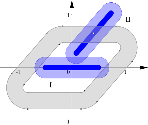
We performed an evaluation of the contribution of tunneling to electrical conductivity. By using a geometrical consideration (Fig. 3), one can conclude that two arbitrary wires I and II will not intersect each other while their shells overlap or touch each other when the center of wire II is situated within the shaded region. Note that the external perimeter of the shaded region limits the excluded area of the discorectangle.Balberg et al. (1984) The area of the shaded region is This conclusion is valid for arbitrary orientations of the wires.
The probability density function (PDF), that the shortest distance between two arbitrary wires equals exactly (), is
| (9) |
The total contribution of all tunnel contacts to the electrical conductivity, , is
The number of wires, for which their centers are located within the shaded area in Fig. 3, is . Hence, the number of pairs that obey the condition , is
the expectation of can be written as
The expectation can be evaluated as
The integration yields
where . Since ,
| (10) |
When ,
| (11) |
When the cutoff distance is , the error in the value of obtained using Eq. (10) is about 1%. This is the reason for our choice of for computations.
Since and , . In the particular case , the electrical conductance is
| (12) |
Naturally, the contribution of tunneling into the electrical conductance is proportional to the square of the number of particles. In addition, the formula includes the ratio of the characteristic tunneling area to the area of the entire system.
III.2 Results of simulation
Figure 4 demonstrates an example of the dependency of the electrical conductance of NWNs, , on the number density, , for different values of the tunneling decay length, , and low values of the junction conductance, , and . This set of parameters can be considered as corresponding to untreated NWNs. For values of the number density , the effect of tunneling on the electrical conductance is negligible. However, the percolation threshold decreases due to tunneling.
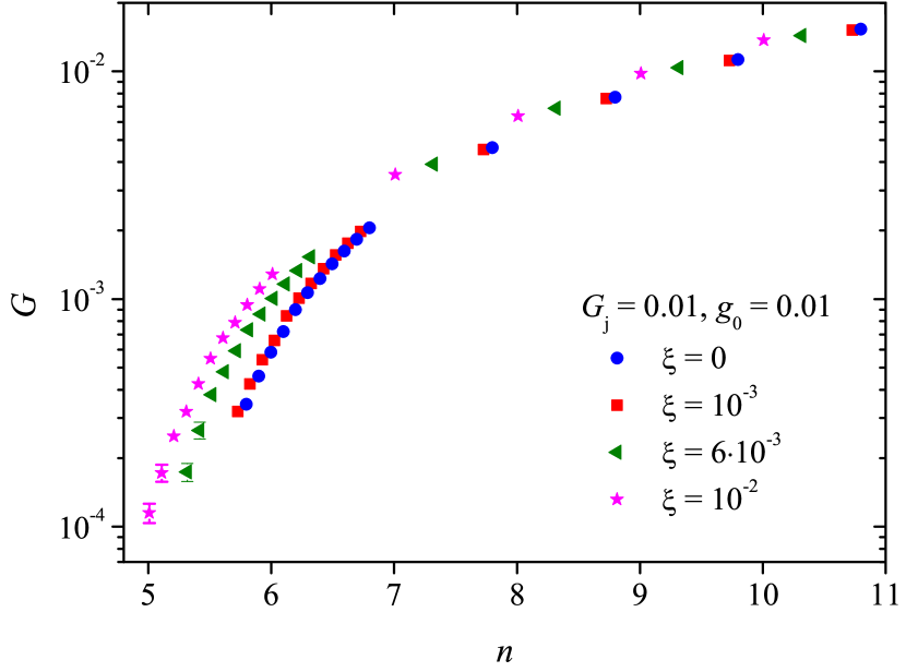
Figure 5 shows the behavior of the electrical conductance of NWNs, , for different values of the tunneling decay length, , and high values of the junction conductance, while the tunneling parameter is low . This case can be treated as corresponding to welded NWNs since . For values of the number density , the effect of the tunneling on the electrical conductance is negligible. However, the percolation threshold decreases due to tunneling.
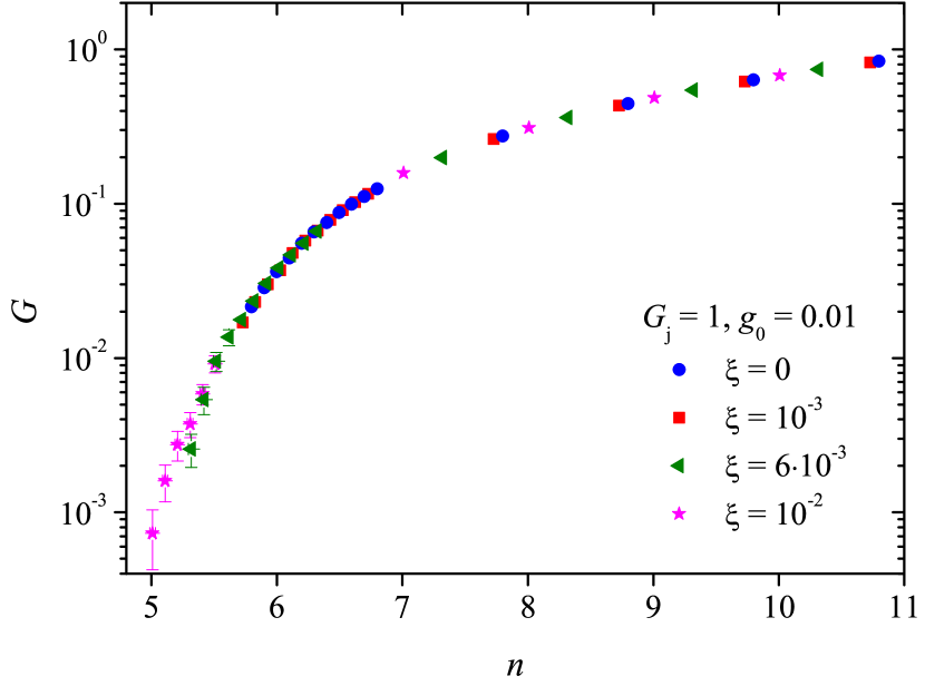
Figure 6 compares the dependencies of the electrical conductances of NWNs, , for different values of the tunneling decay length, , and high values both of the junction conductance and the tunneling parameter, viz., and . This case can also be treated as corresponding to welded NWNs since . The only difference from Fig. 4 is the larger magnitude of the electrical conductance.
IV Conclusion
We have studied both analytically and numerically the impact of tunneling on the electrical conductivities of nanowire networks. A nanowire was represented as a hard conductive core with a soft shell that ensures tunneling occurs when shells belonging to different wires overlap. We found that the tunneling had a negligible effect on the electrical conductivity of dense networks. The analytical consideration evidences that, in the slender rod limit (the aspect ratio of the wires tends to infinity), the contribution of the tunneling into the electrical conductance is .
Acknowledgements.
We acknowledge the funding from the Ministry of Science and Higher Education of the Russian Federation, Project No. 3.959.2017/4.6.References
- Manning et al. (2019) H. G. Manning, C. Gomes da Rocha, C. O’Callaghan, M. S. Ferreira, and J. J. Boland, “The electro-optical performance of silver nanowire networks,” Sci. Rep. 9, 11550 (2019).
- Bae et al. (2012) S. Bae, S. J. Kim, D. Shin, J.-H. Ahn, and B. H. Hong, “Towards industrial applications of graphene electrodes,” Phys. Scr. T146, 014024 (2012).
- Lee et al. (2008) J.-Y. Lee, S. T. Connor, Y. Cui, and P. Peumans, “Solution-processed metal nanowire mesh transparent electrodes,” Nano Lett. 8, 689–692 (2008).
- Madaria et al. (2010) A. R. Madaria, A. Kumar, F. N. Ishikawa, and C. Zhou, “Uniform, highly conductive, and patterned transparent films of a percolating silver nanowire network on rigid and flexible substrates using a dry transfer technique,” Nano Res. 3, 564–573 (2010).
- Garnett et al. (2012) E. C. Garnett, W. Cai, J. J. Cha, F. Mahmood, S. T. Connor, M. G. Christoforo, Y. Cui, M. D. McGehee, and M. L. Brongersma, “Self-limited plasmonic welding of silver nanowire junctions,” Nat. Mater. 11, 241–249 (2012).
- Han et al. (2014) S. Han, S. Hong, J. Ham, J. Yeo, J. Lee, B. Kang, P. Lee, J. Kwon, S. S. Lee, M.-Y. Yang, and S. H. Ko, “Fast plasmonic laser nanowelding for a Cu-nanowire percolation network for flexible transparent conductors and stretchable electronics,” Adv. Mater. 26, 5808–5814 (2014).
- Tokuno et al. (2011) T. Tokuno, M. Nogi, M. Karakawa, J. Jiu, T. T. Nge, Y. Aso, and K. Suganuma, “Fabrication of silver nanowire transparent electrodes at room temperature,” Nano Res. 4, 1215–1222 (2011).
- Xiong et al. (2016) W. Xiong, H. Liu, Y. Chen, M. Zheng, Y. Zhao, X. Kong, Y. Wang, X. Zhang, X. Kong, P. Wang, and L. Jiang, “Highly conductive, air-stable silver nanowire@iongel composite films toward flexible transparent electrodes,” Adv. Mater. 28, 7167–7172 (2016).
- Lee et al. (2013) J. Lee, P. Lee, H. B. Lee, S. Hong, I. Lee, J. Yeo, S. S. Lee, T.-S. Kim, D. Lee, and S. H. Ko, “Room-temperature nanosoldering of a very long metal nanowire network by conducting-polymer-assisted joining for a flexible touch-panel application,” Adv. Funct. Mater. 23, 4171–4176 (2013).
- Lu et al. (2015) H. Lu, D. Zhang, J. Cheng, J. Liu, J. Mao, and W. C. H. Choy, “Locally welded silver nano-network transparent electrodes with high operational stability by a simple alcohol-based chemical approach,” Adv. Funct. Mater. 25, 4211–4218 (2015).
- Liu et al. (2017) Y. Liu, J. Zhang, H. Gao, Y. Wang, Q. Liu, S. Huang, C. F. Guo, and Z. Ren, “Capillary-force-induced cold welding in silver-nanowire-based flexible transparent electrodes,” Nano Lett. 17, 1090–1096 (2017).
- Zhu et al. (2013) S. Zhu, Y. Gao, B. Hu, J. Li, J. Su, Z. Fan, and J. Zhou, “Transferable self-welding silver nanowire network as high performance transparent flexible electrode,” Nanotechnology 24, 335202 (2013).
- Zhao et al. (2019) L. Zhao, S. Yu, X. Li, M. Wu, and L. Li, “High-performance flexible transparent conductive films based on copper nanowires with electroplating welded junctions,” Sol. Energy Mater. Sol. Cells 201, 110067 (2019).
- Bellew et al. (2015) A. T. Bellew, H. G. Manning, C. Gomes da Rocha, M. S. Ferreira, and J. J. Boland, “Resistance of single Ag nanowire junctions and their role in the conductivity of nanowire networks,” ACS Nano 9, 11422–11429 (2015), supporting info DOI: 10.1021/acsnano.5b05469.
- Nguyen et al. (2019) V. H. Nguyen, J. Resende, D. T. Papanastasiou, N. Fontanals, C. Jiménez, D. Muñoz Rojas, and D. Bellet, “Low-cost fabrication of flexible transparent electrodes based on Al doped ZnO and silver nanowire nanocomposites: impact of the network density,” Nanoscale 11, 12097–12107 (2019).
- He et al. (2018) S. He, X. Xu, X. Qiu, Y. He, and C. Zhou, “Conductivity of two-dimensional disordered nanowire networks: Dependence on length-ratio of conducting paths to all nanowires,” J. Appl. Phys. 124, 054302 (2018).
- Lee et al. (2016) E.-J. Lee, Y.-H. Kim, D. K. Hwang, W. K. Choi, and J.-Y. Kim, “Synthesis and optoelectronic characteristics of 20 nm diameter silver nanowires for highly transparent electrode films,” RSC Adv. 6, 11702–11710 (2016).
- Xu et al. (2018) F. Xu, W. Xu, B. Mao, W. Shen, Y. Yu, R. Tan, and W. Song, “Preparation and cold welding of silver nanowire based transparent electrodes with optical transmittances >90% and sheet resistances <10 ohm/sq,” J. Coll. Interf. Sci. 512, 208–218 (2018).
- Žeželj and Stanković (2012) M. Žeželj and I. Stanković, “From percolating to dense random stick networks: Conductivity model investigation,” Phys. Rev. B 86, 134202 (2012).
- O’Callaghan et al. (2016) C. O’Callaghan, C. Gomes da Rocha, H. G. Manning, J. J. Boland, and M. S. Ferreira, “Effective medium theory for the conductivity of disordered metallic nanowire networks,” Phys. Chem. Chem. Phys. 18, 27564–27571 (2016).
- Kumar and Kulkarni (2016) A. Kumar and G. U. Kulkarni, “Evaluating conducting network based transparent electrodes from geometrical considerations,” J. Appl. Phys. 119, 015102 (2016).
- Forró et al. (2018) C. Forró, L. Demkó, S. Weydert, J. Vörös, and K. Tybrandt, “Predictive model for the electrical transport within nanowire networks,” ACS Nano 12, 11080–11087 (2018).
- Kim and Nam (2018) D. Kim and J. Nam, “Systematic analysis for electrical conductivity of network of conducting rods by Kirchhoff’s laws and block matrices,” J. Appl. Phys. 124, 215104 (2018).
- Benda, Cancès, and Lebental (2019) R. Benda, E. Cancès, and B. Lebental, “Effective resistance of random percolating networks of stick nanowires: Functional dependence on elementary physical parameters,” J. Appl. Phys. 126, 044306 (2019).
- Jagota and Scheinfeld (2019) M. Jagota and I. Scheinfeld, “Approximate analytical modeling of random nanowire network conductivity,” (2019), arXiv:1908.10016 [cond-mat.mes-hall] .
- Han et al. (2018) F. Han, T. Maloth, G. Lubineau, R. Yaldiz, and A. Tevtia, “Computational investigation of the morphology, efficiency, and properties of silver nano wires networks in transparent conductive film,” Sci. Rep. 8, 17494 (2018).
- Li and Zhang (2010) J. Li and S.-L. Zhang, “Conductivity exponents in stick percolation,” Phys. Rev. E 81, 021120 (2010).
- Mertens and Moore (2012) S. Mertens and C. Moore, “Continuum percolation thresholds in two dimensions,” Phys. Rev. E 86, 061109 (2012).
- Li and Zhang (2009) J. Li and S.-L. Zhang, “Finite-size scaling in stick percolation,” Phys. Rev. E 80, 040104 (2009).
- Li and Östling (2013) J. Li and M. Östling, “Percolation thresholds of two-dimensional continuum systems of rectangles,” Phys. Rev. E 88, 012101 (2013).
- Li and Östling (2016) J. Li and M. Östling, “Precise percolation thresholds of two-dimensional random systems comprising overlapping ellipses,” Physica A 462, 940–950 (2016).
- Lin and Chen (2019) J. Lin and H. Chen, “Measurement of continuum percolation properties of two-dimensional particulate systems comprising congruent and binary superellipses,” Powder Technol. 347, 17–26 (2019).
- Tarasevich and Eserkepov (2019) Y. Y. Tarasevich and A. V. Eserkepov, “Percolation thresholds for discorectangles: numerical estimation for a range of aspect ratios,” (2019), arXiv:1910.05072 [cond-mat.dis-nn] .
- Balberg (2009) I. Balberg, “Tunnelling and percolation in lattices and the continuum,” J. Phys. D 42, 064003 (2009).
- Sohn et al. (2019) H. Sohn, C. Park, J.-M. Oh, S. W. Kang, and M.-J. Kim, “Silver nanowire networks: Mechano-electric properties and applications,” Materials 12, 2526 (2019).
- Ambrosetti et al. (2010) G. Ambrosetti, C. Grimaldi, I. Balberg, T. Maeder, A. Danani, and P. Ryser, “Solution of the tunneling-percolation problem in the nanocomposite regime,” Phys. Rev. B 81, 155434 (2010).
- Nigro et al. (2013) B. Nigro, C. Grimaldi, M. A. Miller, P. Ryser, and T. Schilling, “Depletion-interaction effects on the tunneling conductivity of nanorod suspensions,” Phys. Rev. E 88, 042140 (2013).
- Simmons (1963) J. G. Simmons, “Generalized formula for the electric tunnel effect between similar electrodes separated by a thin insulating film,” J. Appl. Phys. 34, 1793–1803 (1963).
- Matthews, Hagmann, and Mayer (2018) N. Matthews, M. J. Hagmann, and A. Mayer, “Comment: “Generalized formula for the electric tunnel effect between similar electrodes separated by a thin insulating film” [J. Appl. Phys. 34, 1793 (1963)],” J. Appl.Phys. 123, 136101 (2018).
- Nigro and Grimaldi (2014) B. Nigro and C. Grimaldi, “Impact of tunneling anisotropy on the conductivity of nanorod dispersions,” Phys. Rev. B 90, 094202 (2014).
- Haghgoo et al. (2019) M. Haghgoo, R. Ansari, M. K. Hassanzadeh-Aghdam, and M. Nankali, “Analytical formulation for electrical conductivity and percolation threshold of epoxy multiscale nanocomposites reinforced with chopped carbon fibers and wavy carbon nanotubes considering tunneling resistivity,” Compos. Part A. Appl. Sci. Manuf. 126, 105616 (2019).
- Newman and Ziff (2000) M. E. J. Newman and R. M. Ziff, “Efficient Monte Carlo algorithm and high-precision results for percolation,” Phys. Rev. Lett. 85, 4104–4107 (2000).
- Newman and Ziff (2001) M. E. J. Newman and R. M. Ziff, “Fast Monte Carlo algorithm for site or bond percolation,” Phys. Rev. E 64, 016706 (2001).
- Ponzoni (2019) A. Ponzoni, “The contributions of junctions and nanowires/nanotubes in conductive networks,” Appl.Phys. Lett. 114, 153105 (2019).
- Kumar, Vidhyadhiraja, and Kulkarni (2017) A. Kumar, N. S. Vidhyadhiraja, and G. U. Kulkarni, “Current distribution in conducting nanowire networks,” J. Appl. Phys. 122, 045101 (2017).
- Balberg et al. (1984) I. Balberg, C. H. Anderson, S. Alexander, and N. Wagner, “Excluded volume and its relation to the onset of percolation,” Phys. Rev. B 30, 3933–3943 (1984).